JP3965732B2 - Antireflection film - Google Patents
Antireflection film Download PDFInfo
- Publication number
- JP3965732B2 JP3965732B2 JP22865897A JP22865897A JP3965732B2 JP 3965732 B2 JP3965732 B2 JP 3965732B2 JP 22865897 A JP22865897 A JP 22865897A JP 22865897 A JP22865897 A JP 22865897A JP 3965732 B2 JP3965732 B2 JP 3965732B2
- Authority
- JP
- Japan
- Prior art keywords
- layer
- refractive index
- antireflection
- antireflection film
- film
- Prior art date
- Legal status (The legal status is an assumption and is not a legal conclusion. Google has not performed a legal analysis and makes no representation as to the accuracy of the status listed.)
- Expired - Fee Related
Links
Images



Landscapes
- Transforming Electric Information Into Light Information (AREA)
- Devices For Indicating Variable Information By Combining Individual Elements (AREA)
- Surface Treatment Of Optical Elements (AREA)
- Laminated Bodies (AREA)
Description
【0001】
【発明の属する技術分野】
本発明は、ディスプレイの表示画面の表面に適用される反射防止フィルムに関する。特に、可視光の広波長域で優れた反射防止性能を発揮する反射防止フィルムに関する。
【0002】
【従来の技術】
ディスプレイの多くは、室内外を問わず、外光が入射する環境下で使用されている。ディスプレイに入射した外光は、ディスプレイ内部において正反射され、光源の虚像をディスプレイの表示画面に再生する。このため、蛍光灯等が画面に映り、本来の表示画像を見えにくくなるなどの問題を生じさせる。また、ディスプレイに入射した外光は本来の表示光に混合して表示品質を低下させる。
【0003】
そこで、このような外光のディスプレイ内への入射を防止するため、透明プラスチックフィルム基材の表面に金属酸化物などからなる高屈折率層と低屈折率層を積層した、あるいは透明プラスチックフィルム基材の表面に無機化合物や有機フッ素化合物などの低屈折率層を単層で積層した反射防止効果を有するフィルム、即ち反射防止フィルムをディスプレイ表面上に貼り合わせことなどがなされている。
【0004】
また、これとは別に、透明プラスチックフィルム基材の表面に透明な微粒子を含むコーティング層を形成してその表面を凸凹状とし、それにより外光を乱反射させて同様の効果を得ることがなされている。
【0005】
【発明が解決しようとする課題】
ところで、最近のオフィスのOA化に伴い、コンピューターを使用する頻度が増し、CRTや液晶ディスプレイと相対していることが長時間化している。したがって、外光がディスプレイ内へ入射して反射像等が生じることによる表示品質の低下は、目の疲労など健康障害等を引き起こす要因とも考えられ、これまで以上に可視光の広範囲にわたってより高い反射防止効果を有する反射防止フィルムや、このような反射防止フィルムを備えた光学部材の要求が高まっている。
【0006】
更には、近年ではアウトドアライフの普及に伴い、テレビや液晶ディスプレイを室外で使用する機会が益々増える傾向にあり、表示品質をより向上させて表示画像を明確に認識できるようにするため、可視光の広範囲にわたってより高い反射防止効果を有する反射防止フィルムや、このような反射防止フィルムを備えた光学部材の要求が出てきている。
【0007】
しかしながら、無機化合物や有機化合物の低屈折率物質を単層で形成した従来の反射防止フィルムはU型の分光反射特性を示し、可視光の広範囲にわたり高い反射防止効果を得ることはできない。また、高屈折率層と低屈折率層を交互に積層した多層構成によるものでは、可視光の広範囲で有効な反射防止効果は得られるものの、使用材料が高価なため、コスト上昇が引き起こされるという問題がある。特に、低屈折率層を形成する材料は実用上酸化珪素のみであるため、材料選択の自由度にも制限がきたされ、低屈折率層の形成のためのコスト上昇が避けられないものとなっている。
【0008】
一方、外光のディスプレイ内への入射を防止するため、外光を乱反射させる方法では、ディスプレイ上の画像がぼやけて見えるという問題がある。
【0009】
本発明は、このような問題点に着目してなされたもので、その目的とするところは、より広い波長域で反射率を抑制でき、フレキシビリティーに富み、材料選択の幅が広く、実用性に優れ、安価で且つ容易に得られる反射防止フィルムを提供することを目的とする。
【0010】
本発明者は、上記の目的を達成するため、フィルム基材上に反射防止層を有する反射防止フィルムにおいて、該反射防止層が、そのフィルム基材側から、屈折率が1.80以上の高屈折率層であって光学膜厚(nd)が55nm〜65nmである第一層と、屈折率が1.70以下の低屈折率層であって光学膜厚(nd)が25nm〜40nmである第二層と、屈折率が1.80以上の高屈折率層であって光学膜厚(nd)が110nm〜150nmである第三層と、屈折率が1.70以下の低屈折率層であって光学膜厚(nd)が135nm〜145nmである第四層とが順に積層されたものであり、該第四層が有機樹脂からなることを特徴とする反射防止フィルムを提供する。
【0011】
特に、上記反射防止フィルムにおいて、高屈折率層と低屈折率層との合計の全積層数が、2〜6であるものや、高屈折率層がセラミックス、好ましくはセラミックスが、酸化チタン、酸化ジルコニウム、酸化タンタル、酸化亜鉛、酸化インジウム、酸化ハフニウム、酸化セリウム、酸化錫、酸化ニオブ、酸化イットリウム、酸化イッテリビウム、インジウム・錫酸化物及びこれら2以上の混合物質から選ばれるものを提供する。
【0012】
また、上記反射防止フィルムにおいて、低屈折率層を形成する有機樹脂が、熱硬化性、紫外線硬化性又は電子線硬化性であり、熱可塑性を示すものを提供する。
【0013】
上記反射防止フィルムにおいて、フィルム基材と反射防止層との間に、ハードコート層が形成されているものや、反射防止層の上に撥水・防汚層が形成されているものを提供する。
【0014】
さらに、上記反射防止フィルムを有する光学部材を提供する。
【0015】
このような本発明の反射防止フィルムによれば、フィルム基材上の少なくとも片面に、屈折率が1.80以上の高屈折率層と、屈折率が1.70以下の低屈折率層とを交互に積層した反射防止層が形成されているので、可視光の広範囲にわたる波長域において、優れた反射防止効果を得ることができる。また、この反射防止フィルムを形成する低屈折率層の少なくとも1層が有機樹脂からなるのでフレキシビリティーも高めることができる。さらに、低屈折率層を形成する有機樹脂としては、単一種の有機樹脂に限らず、屈折率が1.70以下である限り、種々の樹脂を使用することができる。したがって、この反射防止フィルムはその材料選択の幅が広く、また、安価に製造できるものとなる。
【0016】
【発明の実施の形態】
以下、本発明の実施の形態に係る反射防止フィルムの例を図面に示し、詳細に説明する。なお、各図中、同一符号は同一又は同等の構成要素を表している。
【0017】
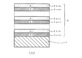
図1から図4は、それぞれ本発明の反射防止フィルムの態様例の層構成を示す断面図である。
【0018】
図1の反射防止フィルム10Aは、フィルム基材1に反射防止層2を形成したもので、反射防止層2は、高屈折率層2a(i)と低屈折率層2b(i)を交互にそれぞれn層積層し(i=1〜n)、低屈折率層2bが最上層となるように構成したものであり、図2は、図1の反射防止フィルム10Aにおいて i=2の態様、即ち、高屈折率層2aと低屈折率層2bとをそれぞれ2層積層した態様を示したものである。
【0019】
この反射防止フィルム10Aにおいて、フィルム基材1は、透明なプラスチックフィルムから形成することが好ましく、ポリメチルメタクリレート、ポリカーボネート、ポリスチレン、ポリエチレンサルファイド、ポリエーテルスルホン、ポリオレフィン、ポリエチレンテレフタレート、ポリエチレンナフタレート、トリアセチルセルロース等を使用でき、これらは当該反射防止フィルム10Aの目的、用途によって適宜選択される。また、その厚さは用途に応じて選定される。
【0020】
反射防止層2は、高屈折率層2aと低屈折率層2bとを交互に所定の光学膜厚nd(屈折率n×形状膜厚d)となるように積層し、かつ低屈折率層2bが最上層となるよう構成したものである。
【0021】
ここで、高屈折率層2aとしては、屈折率nHが1.80以上のものを使用する。高屈折率層2aの屈折率nHが1.80未満であると、反射防止フィルム10Aの反射率を十分に抑制することができない。
【0022】
高屈折率層2aは、屈折率nHが1.80以上である限りその形成材料に特に制限はないが、実用的には、酸化チタン、酸化ジルコニウム、酸化タンタル、酸化亜鉛、酸化インジウム、酸化ハフニウム、酸化セリウム、酸化錫、酸化ニオブ、酸化イットリウム、酸化イッテリビウム、インジウム・錫酸化物等の金属酸化物のいずれか、あるいはこれらを主材料とする混合物質を用いることが好ましい。中でも、酸化亜鉛、酸化インジウム、酸化錫、インジウム・錫及びこれらの混合物質は導電性を有するため、これらから高屈折率層2aを形成すると、反射防止フィルム10Aに反射防止機能に加えて電磁波シールド機能を付与することができるので好ましい。
【0023】
高屈折率層2aは、真空蒸着法、反応性蒸着法、イオンビームアシスト蒸着法、スパッタリング法、イオンプレーティング法、プラズマCVD法などの真空成膜プロセスによって形成することができるが、これに限らずいかなる成膜方法で形成してもよい。
【0024】
一方、低屈折率層2bは、屈折率nLが1.70以下の材料から形成する。低屈折率層2bの屈折率nLが1.70を超えると、反射防止フィルム10Aの反射率を十分に抑制することができない。
【0025】
また、低屈折率層2b(i=1〜n)のうち少なくとも1層、好ましくは全層数の1/2を最多として1〜3層を有機樹脂から形成する。この場合、反射防止層2の最上層(2b(n))に有機樹脂からなる低屈折率層を形成すると、本発明の効果を高く発揮させることができるので好ましい。
【0026】
このような有機樹脂としては、種々の熱硬化性樹脂、紫外線硬化性樹脂、電子線硬化性樹脂等を使用することができ、より具体的には、例えば、有機珪素系、多官能を含むアクリル系、ウレタン系、ポリエステル系、メラミン系等の熱可塑性樹脂をあげることができる。
【0027】
本発明において、低屈折率層2bは、その少なくとも1層を上述のように有機樹脂から形成するが、残りの低屈折率層2bは、金属酸化物から形成してもよく、上述のような有機樹脂から形成してもよい。
【0028】
低屈折率層2bの形成方法には特に制限はなく、例えば、高屈折率層2aと同様に真空成膜プロセスによって成膜することができ、この他、グラビアやスクリーンなどのウエットコートと熱乾燥法、熱硬化法、紫外線照射硬化法、電子線照射硬化法等の成膜プロセスによっても形成することができる。これらは、低屈折率層2bの形成に使用する当該有機樹脂に応じて適宣選択される。また、紫外線硬化法、電子線照射硬化法等を行う場合に、真空中に有機樹脂を加熱気化、或いは超音波によりミスト化して基材に導入し、基材近傍で紫外線、電子線等を照射することにより低屈折率層2bを形成することも可能である。
【0029】
以上のような高屈折率層2aと低屈折率層2bとの合計の全積層数は、生産性、コスト等を考慮すると少ない方がよいが、通常2〜6層とすることが好ましい。これにより本発明の反射防止フィルムの反射特性を、一般的に可視光とされる400nm〜700nmの範囲中、人間の目の感度の比較的高い450nm〜650nmの範囲において平均反射率を3%以下、さらには1%以下とすることができる。
【0030】
本発明において、上述の反射防止層2以外の構成は、公知の反射防止フィルムと同様に構成することができるが、好ましくは、図3に示す反射防止フィルム10B又は図4に示す反射防止フィルム10Cのように、撥水・防汚層3やハードコート層4を設ける。
【0031】
この撥水・防汚層3は、反射防止層2の表面を保護し、更に防汚性を高めるために反射防止層2上に形成されるものであり、その形成材料としては、透明性を有し、要求性能が満たされる限り、いかなる材料でも制限なく使用することができる。例えば、疎水基を有する化合物、より具体的には、フルオロカーボンやパーフルオロシラン等、またこれらの高分子化合物等を好ましく使用することができる。また、指紋拭き取り汚性向上のためには、メチル基の様な撥油性を有する高分子化合物が好適である。
【0032】
撥水・防汚層3の形成方法としては、当該形成材料に応じて真空蒸着法、スパッタリング法、イオンプレーティング法、プラズマCVD法、プラズマ重合法などの真空成膜プロセスや、マイクログラビア、スクリーン、ディップ等のウェットプロセスの各種コーティング方法を用いることができる。
【0033】
撥水・防汚層3の厚さは反射防止層2の機能を損なわないよう設定することが必要であり、通常、形状膜厚を50nm以下とすることが好ましい。
【0034】
ハードコート層4は、反射防止フィルムに所望の硬さを付与するため、必要に応じて設けられる。したがってこのハードコート層4としては、透明性を有し、適度な硬度を有する層を形成することが好ましく、その形成材料には特に限定はない。例えば、電離放射線や紫外線照射による硬化樹脂や熱硬化性樹脂を使用できる。特に、紫外線照射硬化型のアクリル系や有機珪素系の樹脂や、熱硬化型のポリシロキサン樹脂が好適である。これらの樹脂は、フィルム基材1と屈折率が同等もしくは近似していることがより好ましいが、膜厚が3μm以上の場合には特にこの点も必要ない。
【0035】
また、ハードコート層4を形成するにあたり、塗布方法に制限はないが、表面平滑に且つ均一に形成することが好ましい。
【0036】
ハードコート層4には平均粒子径0.01〜3μmの透明な無機あるいは有機の超微粒子を混合分散させてもよい。これによりアンチグレアと呼ばれる光拡散性の処理を施すことができる。そしてこの光拡散性の処理を施したハードコート層4上に反射防止層2を形成することにより、画像のぼやけが小さくなり、単なる光拡散性の処理を施した場合よりも画像が明瞭になる。これらの超微粒子は、透明であれば特に限定されるものではないが、屈折率1.6以下の低屈折率材料からなる粒子が好ましく、例えば、酸化珪素粒子、弗化マグネシウム粒子等が安定性、耐熱性等の点から好適である。
【0037】
本発明の反射防止フィルムは、従来の反射防止フィルムと同様に使用することができ、例えば、粘着剤、接着剤等を用いてガラス板、プラスチック板、偏向板等と貼り合わせることにより反射防止性を有する光学部材を得ることができる。そこで、本発明は、このような光学部材も包含する。
【0038】
【実施例】
以下、本発明を実施例に基づいて具体的に説明する。
【0039】
実施例1
図2に示した層構成の反射防止フィルムを次のように作製した。
【0040】
透明なフィルム基材1として、ポリエチレンテレフタレート(PET)フィルム(厚さ100μm)上に、以下に示す表1の層構成の反射防止層2を形成し、反射防止フィルムとした。この場合、まず、プラズマアシスト蒸着法により、フィルム基材1上に酸化チタンからなる高屈折率層2aと酸化珪素からなる低屈折率層2bとを積層し、更に最上層(第4層)の低屈折率層2bをなす有機樹脂層として、シリコーン系樹脂を熱硬化法により形成した。
【0041】
反射防止層2を構成する各層の屈折率及び光学膜厚ndを表1に示す。なお、各層の光学膜厚は、光学式の膜厚モニターにより監視し、目的光量値に達した時に成膜を止めることにより所定の値に制御した。
【0042】
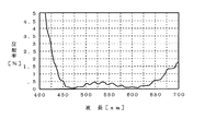
得られた反射防止フィルムの絶対反射測定による分光反射特性を図5に示す。同図から、この反射防止フィルムは光の波長の450nm〜650nm以上にわたって反射率が0.5%以下であり、高い反射防止性を広波長域で有することが確認できた。
【0043】
【表1】
反射防止フィルムの層構成
基材フィルム:PETフィルム(厚さ100μm)
反射防止層:
第1層 高屈折率層:TiO2 (nH1=2.30,nd=65nm)
第2層 低屈折率層:SiO2 (nL1=1.46,nd=35nm)
第3層 高屈折率層:TiO2 (nH2=2.30,nd=110nm)
第4層 低屈折率層:シリコーン系樹脂 (nL2=1.50,nd=145nm)
【0044】
実施例2
透明なフィルム基材1としてトリアセチルセルロースフィルム(厚さ80μm)を使用し、その上に、まず透明なハードコート層4として単官能性アクリル樹脂を紫外線照射硬化法により形成し、次に表2に示す層構成の反射防止層2を形成した。この場合、まず、酸化チタンからなる高屈折率層2aと、酸化珪素からなる低屈折率層2bとを実施例1と同様にしてプラズマアシスト蒸着法により形成し、更に最上層(第4層)の低屈折率層2bをなす有機樹脂層としてアクリル系樹脂を紫外線照射法により形成した。
【0045】
反射防止層2を構成する各層の屈折率及び光学膜厚ndを表2に示す。また、得られた反射防止フィルムの絶対反射測定による分光反射特性を図6に示す。同図から、この反射防止フィルムは光の波長の450nm〜650nm以上にわたって反射率が0.5%以下であり、高い反射防止性を広波長域で有することが確認できた。
【0046】
【表2】
反射防止フィルムの層構成
基材フィルム:トリアセチルセルロースフィルム(厚さ80μm)
ハードコート層:アクリル系樹脂(nH1=1.50,厚さ5μm)
反射防止層:
第1層 高屈折率層:TiO2 (nH1=2.30,nd=60nm)
第2層 低屈折率層:SiO2 (nL1=1.46,nd=40nm)
第3層 高屈折率層:TiO2 (nH2=2.30,nd=120nm)
第4層 低屈折率層:アクリル系樹脂 (nL2=1.50,nd=140nm)
【0047】
実施例3
透明なフィルム基材1としてPETフィルム(厚さ100μm)を使用し、その上に、表3に示す層構成の反射防止層2を形成した。この場合、まず酸化チタンからなる高屈折率層2aと、酸化珪素からなる低屈折率層2bとを実施例1と同様にしてプラズマアシスト蒸着法により形成し、更に最上層(第4層)の低屈折率層2bをなす有機樹脂層としてシリコーン系樹脂を紫外線照射硬化法により形成した。
【0048】
更にこの上に撥水・防汚層3としてパーフルオロシランをプラズマCVD法により成膜し、反射防止フィルムとした。
【0049】
得られた反射防止フィルムの反射防止層2を構成する各層の屈折率及び光学膜厚ndを表3に示す。また、得られた反射防止フィルムの絶対反射測定による分光反射特性を測定したところ、前述の実施例1の図5とほとんど変わらず、光の波長の450nm〜650nm以上にわたって反射率が0.5%以下であり、高い反射防止性を広波長域で有することが確認できた。
【0050】
【表3】
反射防止フィルムの層構成
基材フィルム:PETフィルム(厚さ100μm)
反射防止層:
第1層 高屈折率層:TiO2 (nH1=2.30,nd=65nm)
第2層 低屈折率層:SiO2 (nL1=1.46,nd=35nm)
第3層 高屈折率層:TiO2 (nH2=2.30,nd=110nm)
第4層 低屈折率層:シリコーン系樹脂 (nL2=1.50,nd=145nm)
撥水・防汚層:パーフルオロシラン(厚さ0.01μm)
【0051】
実施例4
透明なフィルム基材1としてトリアセチルセルロースフィルム(厚さ80μm)を使用し、その上に、まず透明なハードコート層4として有機ケイ素系樹脂を紫外線照射硬化法により形成し、次に表4に示す層構成の反射防止層2を形成した。この場合、まず、酸化チタンからなる高屈折率層2aと、酸化珪素からなる低屈折率層2bとを実施例1と同様にしてプラズマアシスト蒸着法により形成し、更に最上層(第4層)の低屈折率層2bをなす有機樹脂層としてアクリル系樹脂を電子線照射硬化法により形成した。
【0052】
反射防止層2を構成する各層の屈折率及び光学膜厚ndを表4に示す。また、得られた反射防止フィルムの絶対反射測定による分光反射特性を測定したところ、前述の実施例2の図6とほとんど変わらず、光の波長の450nm〜650nm以上にわたって反射率が0.5%以下であり、高い反射防止性を広波長域で有することが確認できた。
【0053】
【表4】
反射防止フィルムの層構成
基材フィルム:トリアセチルセルロースフィルム(厚さ80μm)
ハードコート層:有機ケイ素系樹脂(nH1=1.49,厚さ5μm)
反射防止層:
第1層 高屈折率層:TiO2 (nH1=2.30,nd=60nm)
第2層 低屈折率層:SiO2 (nL1=1.46,nd=40nm)
第3層 高屈折率層:TiO2 (nH2=2.30,nd=120nm)
第4層 低屈折率層:アクリル系樹脂 (nL2=1.50,nd=140nm)
【0054】
実施例5
透明なフィルム基材1としてPETフィルム(厚さ100μm)を使用し、その上に、表5に示す層構成の反射防止層2を形成した。この場合、まず酸化インジウム酸化錫混合物(ITO)からなる高屈折率層2aと、酸化珪素からなる低屈折率層2bとを実施例1と同様にしてプラズマアシスト蒸着法により形成し、更に最上層(第4層)の低屈折率層2bをなす有機樹脂層として熱可塑性アクリル樹脂を塗布形成した。
【0055】
更にこの上に撥水・防汚層3としてパーフルオロシランをプラズマCVD法により成膜し、反射防止フィルムとした。
【0056】
得られた反射防止フィルムの反射防止層2を構成する各層の屈折率及び光学膜厚ndを表5に示す。また、得られた反射防止フィルムの絶対反射測定による分光反射特性を測定したところ、前述の実施例1の図5とほとんど変わらず、光の波長の450nm〜650nm以上にわたって反射率が0.5%以下であり、高い反射防止性を広波長域で有することが確認できた。
【0057】
また、電磁波シールド性は、周波数100MHzで30dBの減衰があり、良好なシールド性を示すことが確認できた。
【0058】
【表5】
反射防止フィルムの層構成
基材フィルム:PETフィルム(厚さ100μm)
反射防止層:
第1層 高屈折率層:ITO (nH1=2.10,nd=55nm)
第2層 低屈折率層:SiO2 (nL1=1.46,nd=25nm)
第3層 高屈折率層:ITO (nH2=2.10,nd=150nm)
第4層 低屈折率層:熱可塑性アクリル系樹脂
(nL2=1.50,nd=135nm)
撥水・防汚層:パーフルオロシラン(厚さ0.01μm)
【0059】
比較例1
透明なフィルム基材1としてPETフィルム(厚さ100μm)を使用し、その上に反射防止層2として、低屈折率層2bに相当する多官能基アクリル樹脂の単層を紫外線照射硬化法により形成し、比較例の反射防止フィルムとした。
【0060】
この多官能基アクリル樹脂層の屈折率及び光学膜圧ndは表6に示す通りであった。また、得られた反射防止フィルムの絶対反射測定による分光反射特性を図7に示す。同図から、この比較例の反射防止フィルムは、実施例1〜5の反射防止フィルムと比較して、反射率が明らかに大きく、また、反射防止性を示す波長域が実施例に比して狭かった。
【0061】
【表6】
反射防止フィルムの層構成
基材フィルム:PETフィルム(厚さ100μm)
反射防止層:
低屈折率層:多官能基アクリル樹脂 (nL1=1.50,nd=138nm)
【0062】
【発明の効果】
本発明によれば、フィルム基材上の少なくとも片面に、屈折率が1.80以上の高屈折率層と、屈折率が1.70以下の低屈折率層とを交互に積層して反射防止層を形成し、この反射防止層の低屈折率層のうち少なくとも1層を有機樹脂から形成するので、広い波長域で低い反射率を有し、フレキシビリティー、材料の選択性に優れた、反射防止フィルムを得ることができ、またこのような反射防止フィルムを安価に提供することができる。
【0063】
更に、反射防止層の形成に導電性を有する金属酸化物を用いることにより、本発明の反射防止フィルムに、反射防止効果に加えて導電性や帯電防止性を付加することができ、また最表面に撥水・防汚層を形成することにより、防汚性も付与でき、より高機能化し、実用性に富む反射防止フィルムを得ることができる。
【0064】
また、本発明の反射防止フィルムをガラス板などと貼り合わせるなどにより光学部材を形成することができるが、かかる光学部材をディスプレイに用いることによって、表示品質が向上し、表示画像がより明確に認識できるようになる。
【図面の簡単な説明】
【図1】本発明の反射防止フィルムの層構成図である。
【図2】本発明の反射防止フィルムの層構成図である。
【図3】本発明の反射防止フィルムの他の態様の層構成図である。
【図4】実施例の反射防止フィルムの他の態様の層構成図である。
【図5】実施例1の反射防止フィルムの絶対反射測定による分光反射スペクトルである。
【図6】実施例2の反射防止フィルムの絶対反射測定による分光反射スペクトルである。
【図7】比較例1の反射防止フィルムの絶対反射測定による分光反射スペクトルである。
【符号の説明】
1 フィルム基材
2 反射防止層
2a 高屈折率層
2b 低屈折率層
3 撥水・防汚層
4 ハードコート層
10A、10B、10C 反射防止フィルム[0001]
BACKGROUND OF THE INVENTION
The present invention relates to an antireflection film applied to the surface of a display screen of a display. In particular, the present invention relates to an antireflection film that exhibits excellent antireflection performance in a wide wavelength range of visible light.
[0002]
[Prior art]
Many displays are used in an environment where external light is incident, whether indoors or outdoors. External light incident on the display is regularly reflected inside the display, and a virtual image of the light source is reproduced on the display screen of the display. For this reason, fluorescent lamps and the like are reflected on the screen, which causes problems such as making it difficult to see the original display image. Also, the external light incident on the display is mixed with the original display light to deteriorate the display quality.
[0003]
Therefore, in order to prevent such external light from entering the display, a transparent plastic film substrate is formed by laminating a high refractive index layer and a low refractive index layer made of a metal oxide or the like on the surface of a transparent plastic film substrate. A film having an antireflection effect obtained by laminating a single layer of a low refractive index layer such as an inorganic compound or an organic fluorine compound on the surface of a material, that is, an antireflection film is bonded to the display surface.
[0004]
Separately from this, a coating layer containing transparent fine particles is formed on the surface of the transparent plastic film substrate to make the surface uneven, thereby causing the same effect by irregularly reflecting external light. Yes.
[0005]
[Problems to be solved by the invention]
By the way, with the recent office automation of office automation, the frequency of using a computer has increased, and it has become a long time to be opposed to a CRT or a liquid crystal display. Therefore, the deterioration of display quality due to the incident of external light into the display and the generation of reflected images, etc. is also considered to be a cause of health problems such as eye fatigue, and higher reflection over a wider range of visible light than ever before. There is an increasing demand for an antireflection film having a prevention effect and an optical member provided with such an antireflection film.
[0006]
Furthermore, in recent years, with the spread of outdoor life, there has been an increasing tendency to use TVs and liquid crystal displays outdoors. In order to improve display quality and make it possible to clearly recognize display images, visible light Therefore, there is a demand for an antireflection film having a higher antireflection effect over a wide range of the above and an optical member provided with such an antireflection film.
[0007]
However, a conventional antireflection film in which a low refractive index material such as an inorganic compound or an organic compound is formed as a single layer exhibits U-shaped spectral reflection characteristics, and a high antireflection effect cannot be obtained over a wide range of visible light. In addition, with a multilayer structure in which high refractive index layers and low refractive index layers are alternately stacked, an effective antireflection effect can be obtained over a wide range of visible light, but the cost is increased because the materials used are expensive. There's a problem. In particular, since the material for forming the low refractive index layer is practically only silicon oxide, the degree of freedom in selecting the material has been limited, and an increase in cost for forming the low refractive index layer is inevitable. ing.
[0008]
On the other hand, there is a problem that the image on the display looks blurred in the method of irregularly reflecting the external light in order to prevent the external light from entering the display.
[0009]
The present invention has been made paying attention to such problems, and the object of the present invention is to be able to suppress the reflectance in a wider wavelength range, to be highly flexible, to have a wide range of material selection, and to be practically used. An object of the present invention is to provide an antireflection film which is excellent in properties, inexpensive and easily obtained.
[0010]
In order to achieve the above object, the inventor of the present invention provides an antireflection film having an antireflection layer on a film substrate , wherein the antireflection layer has a refractive index of 1.80 or more from the film substrate side. A first refractive index layer having an optical film thickness (nd) of 55 nm to 65 nm and a low refractive index layer having a refractive index of 1.70 or less and an optical film thickness (nd) of 25 nm to 40 nm. A second layer , a high refractive index layer having a refractive index of 1.80 or more and a third layer having an optical film thickness (nd) of 110 nm to 150 nm, and a low refractive index layer having a refractive index of 1.70 or less. A fourth layer having an optical film thickness (nd) of 135 nm to 145 nm is sequentially laminated , and the fourth layer is made of an organic resin.
[0011]
In particular, in the antireflection film, the total number of layers of the high refractive index layer and the low refractive index layer is 2 to 6, or the high refractive index layer is ceramic, preferably ceramic is titanium oxide, oxidation Provided is one selected from zirconium, tantalum oxide, zinc oxide, indium oxide, hafnium oxide, cerium oxide, tin oxide, niobium oxide, yttrium oxide, ytterbium oxide, indium / tin oxide, and a mixture of two or more thereof.
[0012]
In the antireflection film, the organic resin forming the low refractive index layer is thermosetting, ultraviolet curable, or electron beam curable, and exhibits thermoplasticity.
[0013]
In the antireflection film, a film having a hard coat layer formed between the film base and the antireflection layer, or a film having a water-repellent / antifouling layer formed on the antireflection layer is provided. .
[0014]
Furthermore, the optical member which has the said antireflection film is provided.
[0015]
According to such an antireflection film of the present invention, a high refractive index layer having a refractive index of 1.80 or more and a low refractive index layer having a refractive index of 1.70 or less are formed on at least one surface of the film substrate. Since the antireflection layers laminated alternately are formed, an excellent antireflection effect can be obtained in a wide wavelength range of visible light. In addition, since at least one of the low refractive index layers forming the antireflection film is made of an organic resin, flexibility can be improved. Furthermore, the organic resin forming the low refractive index layer is not limited to a single type of organic resin, and various resins can be used as long as the refractive index is 1.70 or less. Therefore, this antireflection film has a wide range of material selection and can be manufactured at low cost.
[0016]
DETAILED DESCRIPTION OF THE INVENTION
Hereinafter, an example of an antireflection film according to an embodiment of the present invention will be described in detail with reference to the drawings. In each figure, the same numerals indicate the same or equivalent components.
[0017]
FIG. 1 to FIG. 4 are cross-sectional views showing the layer structure of an embodiment of the antireflection film of the present invention.
[0018]
An antireflection film 10A shown in FIG. 1 is obtained by forming an
[0019]
In this antireflection film 10A, the
[0020]
The
[0021]
Here, the high-refractive index layer 2a, the refractive index n H is to use a 1.80 or more. When the refractive index n H of the high refractive index layer 2a is less than 1.80, the reflectance of the antireflection film 10A cannot be sufficiently suppressed.
[0022]
The material of the high refractive index layer 2a is not particularly limited as long as the refractive index n H is 1.80 or more, but practically, titanium oxide, zirconium oxide, tantalum oxide, zinc oxide, indium oxide, oxide It is preferable to use one of metal oxides such as hafnium, cerium oxide, tin oxide, niobium oxide, yttrium oxide, ytterbium oxide, indium / tin oxide, or a mixed material containing these as main materials. Among these, since zinc oxide, indium oxide, tin oxide, indium / tin, and mixed materials thereof have conductivity, when the high refractive index layer 2a is formed therefrom, the antireflection film 10A has an antireflection function in addition to the antireflection function. Since a function can be provided, it is preferable.
[0023]
The high refractive index layer 2a can be formed by a vacuum film formation process such as a vacuum deposition method, a reactive deposition method, an ion beam assisted deposition method, a sputtering method, an ion plating method, a plasma CVD method, but is not limited thereto. The film may be formed by any film forming method.
[0024]
On the other hand, the low refractive index layer 2b is formed of a material having a refractive index n L of 1.70 or less. When the refractive index n L of the low refractive index layer 2b exceeds 1.70, the reflectance of the antireflection film 10A cannot be sufficiently suppressed.
[0025]
In addition, at least one of the low refractive index layers 2b (i = 1 to n), preferably 1 to 3 layers is formed from an organic resin, with ½ of the total number being the largest. In this case, it is preferable to form a low refractive index layer made of an organic resin in the uppermost layer (2b (n)) of the
[0026]
As such an organic resin, various thermosetting resins, ultraviolet curable resins, electron beam curable resins, and the like can be used. More specifically, for example, organic silicon-based and polyfunctional acrylics are used. Examples thereof include thermoplastic resins such as those based on urethane, urethane, polyester, and melamine.
[0027]
In the present invention, at least one layer of the low refractive index layer 2b is formed from an organic resin as described above, but the remaining low refractive index layer 2b may be formed from a metal oxide, as described above. You may form from organic resin.
[0028]
The method for forming the low refractive index layer 2b is not particularly limited. For example, the low refractive index layer 2b can be formed by a vacuum film formation process in the same manner as the high refractive index layer 2a. It can also be formed by a film forming process such as a method, a heat curing method, an ultraviolet irradiation curing method, an electron beam irradiation curing method. These are appropriately selected according to the organic resin used for forming the low refractive index layer 2b. In addition, when performing ultraviolet curing method, electron beam irradiation curing method, etc., organic resin is vaporized by heating or misted by ultrasonic waves and introduced into the substrate, and irradiated with ultraviolet rays, electron beam, etc. near the substrate. By doing so, it is also possible to form the low refractive index layer 2b.
[0029]
The total number of stacked layers of the high refractive index layer 2a and the low refractive index layer 2b as described above is preferably small in consideration of productivity, cost, and the like, but usually 2 to 6 layers are preferable. As a result, the reflection characteristics of the antireflection film of the present invention are such that the average reflectance is 3% or less in the range of 450 nm to 650 nm, which is relatively high in human eye sensitivity, in the range of 400 nm to 700 nm, which is generally regarded as visible light. Further, it can be made 1% or less.
[0030]
In the present invention, configurations other than the above-described
[0031]
The water repellent /
[0032]
As a method for forming the water repellent /
[0033]
The thickness of the water repellent /
[0034]
The
[0035]
In forming the
[0036]
In the
[0037]
The antireflection film of the present invention can be used in the same manner as a conventional antireflection film. For example, the antireflection film is bonded to a glass plate, a plastic plate, a deflection plate, or the like using an adhesive, an adhesive, or the like. An optical member having the following can be obtained. Therefore, the present invention includes such an optical member.
[0038]
【Example】
Hereinafter, the present invention will be specifically described based on examples.
[0039]
Example 1
The antireflection film having the layer structure shown in FIG. 2 was produced as follows.
[0040]
As a
[0041]
Table 1 shows the refractive index and optical film thickness nd of each layer constituting the
[0042]
Spectral reflection characteristics of the obtained antireflection film by absolute reflection measurement are shown in FIG. From this figure, it was confirmed that this antireflection film has a reflectance of 0.5% or less over a wavelength range of 450 nm to 650 nm and has high antireflection properties in a wide wavelength region.
[0043]
[Table 1]
Layer structure of antireflection film
Base film: PET film (100 μm thick)
Antireflection layer:
First layer High refractive index layer: TiO 2 (n H1 = 2.30, nd = 65 nm)
Second layer Low refractive index layer: SiO 2 (n L1 = 1.46, nd = 35 nm)
Third layer High refractive index layer: TiO 2 (n H2 = 2.30, nd = 110 nm)
Fourth layer Low refractive index layer: Silicone resin (n L2 = 1.50, nd = 145 nm)
[0044]
Example 2
A triacetyl cellulose film (thickness: 80 μm) is used as the
[0045]
Table 2 shows the refractive index and optical film thickness nd of each layer constituting the
[0046]
[Table 2]
Layer structure of antireflection film
Base film: Triacetyl cellulose film (thickness 80 μm)
Hard coat layer: acrylic resin (n H1 = 1.50,
Antireflection layer:
First layer High refractive index layer: TiO 2 (n H1 = 2.30, nd = 60 nm)
Second layer Low refractive index layer: SiO 2 (n L1 = 1.46, nd = 40 nm)
Third layer High refractive index layer: TiO 2 (n H2 = 2.30, nd = 120 nm)
Fourth layer Low refractive index layer: Acrylic resin (n L2 = 1.50, nd = 140 nm)
[0047]
Example 3
A PET film (thickness: 100 μm) was used as the
[0048]
Further, perfluorosilane was deposited thereon as a water repellent /
[0049]
Table 3 shows the refractive index and optical film thickness nd of each layer constituting the
[0050]
[Table 3]
Layer structure of antireflection film
Base film: PET film (100 μm thick)
Antireflection layer:
First layer High refractive index layer: TiO 2 (n H1 = 2.30, nd = 65 nm)
Second layer Low refractive index layer: SiO 2 (n L1 = 1.46, nd = 35 nm)
Third layer High refractive index layer: TiO 2 (n H2 = 2.30, nd = 110 nm)
Fourth layer Low refractive index layer: Silicone resin (n L2 = 1.50, nd = 145 nm)
Water repellent / antifouling layer: Perfluorosilane (thickness 0.01 μm)
[0051]
Example 4
A triacetyl cellulose film (thickness: 80 μm) is used as the
[0052]
Table 4 shows the refractive index and the optical film thickness nd of each layer constituting the
[0053]
[Table 4]
Layer structure of antireflection film
Base film: Triacetyl cellulose film (thickness 80 μm)
Hard coat layer: organosilicon resin (n H1 = 1.49,
Antireflection layer:
First layer High refractive index layer: TiO 2 (n H1 = 2.30, nd = 60 nm)
Second layer Low refractive index layer: SiO 2 (n L1 = 1.46, nd = 40 nm)
Third layer High refractive index layer: TiO 2 (n H2 = 2.30, nd = 120 nm)
Fourth layer Low refractive index layer: Acrylic resin (n L2 = 1.50, nd = 140 nm)
[0054]
Example 5
A PET film (thickness: 100 μm) was used as the
[0055]
Further, perfluorosilane was deposited thereon as a water repellent /
[0056]
Table 5 shows the refractive index and optical film thickness nd of each layer constituting the
[0057]
In addition, the electromagnetic wave shielding property was confirmed to be good shielding property with an attenuation of 30 dB at a frequency of 100 MHz.
[0058]
[Table 5]
Layer structure of antireflection film
Base film: PET film (100 μm thick)
Antireflection layer:
First layer High refractive index layer: ITO (n H1 = 2.10, nd = 55 nm)
Second layer Low refractive index layer: SiO 2 (n L1 = 1.46, nd = 25 nm)
Third layer High refractive index layer: ITO (n H2 = 2.10, nd = 150 nm)
Fourth layer Low refractive index layer: Thermoplastic acrylic resin
(n L2 = 1.50, nd = 135 nm)
Water repellent / antifouling layer: Perfluorosilane (thickness 0.01 μm)
[0059]
Comparative Example 1
A PET film (thickness: 100 μm) is used as the
[0060]
The refractive index and optical film pressure nd of this polyfunctional acrylic resin layer were as shown in Table 6. Moreover, the spectral reflection characteristic by the absolute reflection measurement of the obtained antireflection film is shown in FIG. From the same figure, the antireflection film of this comparative example is clearly larger in reflectance than the antireflection films of Examples 1 to 5, and the wavelength range showing antireflection properties is compared to that of the examples. It was narrow.
[0061]
[Table 6]
Layer structure of antireflection film
Base film: PET film (100 μm thick)
Antireflection layer:
Low refractive index layer: polyfunctional acrylic resin (n L1 = 1.50, nd = 138 nm)
[0062]
【The invention's effect】
According to the present invention, on at least one surface of the film substrate, an antireflective film is formed by alternately laminating a high refractive index layer having a refractive index of 1.80 or more and a low refractive index layer having a refractive index of 1.70 or less. Since the layer is formed and at least one of the low refractive index layers of the antireflection layer is formed from an organic resin, it has a low reflectance in a wide wavelength range, and has excellent flexibility and material selectivity. An antireflection film can be obtained, and such an antireflection film can be provided at low cost.
[0063]
Furthermore, by using a conductive metal oxide for forming the antireflection layer, the antireflection film of the present invention can be added with conductivity and antistatic properties in addition to the antireflection effect, and the outermost surface. By forming a water-repellent / anti-fouling layer on the anti-fouling layer, it is possible to impart anti-fouling properties, and to obtain an anti-reflection film that is more functional and practical.
[0064]
In addition, an optical member can be formed by bonding the antireflection film of the present invention to a glass plate or the like, but by using such an optical member for a display, display quality is improved and a display image is recognized more clearly. become able to.
[Brief description of the drawings]
FIG. 1 is a layer configuration diagram of an antireflection film of the present invention.
FIG. 2 is a layer configuration diagram of an antireflection film of the present invention.
FIG. 3 is a layer configuration diagram of another embodiment of the antireflection film of the present invention.
FIG. 4 is a layer configuration diagram of another aspect of the antireflection film of the example.
5 is a spectral reflection spectrum obtained by measuring absolute reflection of the antireflection film of Example 1. FIG.
6 is a spectral reflection spectrum obtained by measuring absolute reflection of the antireflection film of Example 2. FIG.
7 is a spectral reflection spectrum obtained by absolute reflection measurement of the antireflection film of Comparative Example 1. FIG.
[Explanation of symbols]
DESCRIPTION OF
Claims (10)
Priority Applications (1)
| Application Number | Priority Date | Filing Date | Title |
|---|---|---|---|
| JP22865897A JP3965732B2 (en) | 1997-08-25 | 1997-08-25 | Antireflection film |
Applications Claiming Priority (1)
| Application Number | Priority Date | Filing Date | Title |
|---|---|---|---|
| JP22865897A JP3965732B2 (en) | 1997-08-25 | 1997-08-25 | Antireflection film |
Publications (2)
| Publication Number | Publication Date |
|---|---|
| JPH1164602A JPH1164602A (en) | 1999-03-05 |
| JP3965732B2 true JP3965732B2 (en) | 2007-08-29 |
Family
ID=16879792
Family Applications (1)
| Application Number | Title | Priority Date | Filing Date |
|---|---|---|---|
| JP22865897A Expired - Fee Related JP3965732B2 (en) | 1997-08-25 | 1997-08-25 | Antireflection film |
Country Status (1)
| Country | Link |
|---|---|
| JP (1) | JP3965732B2 (en) |
Cited By (2)
| Publication number | Priority date | Publication date | Assignee | Title |
|---|---|---|---|---|
| WO2010090184A1 (en) | 2009-02-03 | 2010-08-12 | 凸版印刷株式会社 | Phase type diffraction element, manufacturing method thereof, and image capture device |
| WO2010095568A1 (en) | 2009-02-20 | 2010-08-26 | 凸版印刷株式会社 | Phase-type diffraction element, manufacturing method thereof, and image pickup apparatus |
Families Citing this family (6)
| Publication number | Priority date | Publication date | Assignee | Title |
|---|---|---|---|---|
| KR20010068812A (en) * | 2000-01-10 | 2001-07-23 | 정상택 | Multi cotainglense |
| JP3510845B2 (en) * | 2000-08-29 | 2004-03-29 | Hoya株式会社 | Optical member having antireflection film |
| JP2003215309A (en) * | 2001-04-17 | 2003-07-30 | Sony Corp | Anti-reflection film and plastic substrate with anti-reflection layer |
| JP2006171647A (en) * | 2004-12-20 | 2006-06-29 | Asahi Glass Co Ltd | Antireflection body and display device using the same |
| JP4966924B2 (en) | 2008-07-16 | 2012-07-04 | 日東電工株式会社 | Transparent conductive film, transparent conductive laminate and touch panel, and method for producing transparent conductive film |
| EP4145186B1 (en) * | 2020-05-01 | 2025-10-29 | Nikon-Essilor Co., Ltd. | Optical member |
-
1997
- 1997-08-25 JP JP22865897A patent/JP3965732B2/en not_active Expired - Fee Related
Cited By (2)
| Publication number | Priority date | Publication date | Assignee | Title |
|---|---|---|---|---|
| WO2010090184A1 (en) | 2009-02-03 | 2010-08-12 | 凸版印刷株式会社 | Phase type diffraction element, manufacturing method thereof, and image capture device |
| WO2010095568A1 (en) | 2009-02-20 | 2010-08-26 | 凸版印刷株式会社 | Phase-type diffraction element, manufacturing method thereof, and image pickup apparatus |
Also Published As
| Publication number | Publication date |
|---|---|
| JPH1164602A (en) | 1999-03-05 |
Similar Documents
| Publication | Publication Date | Title |
|---|---|---|
| US12455403B2 (en) | Optical laminate, article and method of manufacturing optical laminate | |
| JP6780229B2 (en) | How to select anti-reflective film, display device and anti-reflective film for display device | |
| JP2013156523A (en) | Substrate | |
| JPH11258405A (en) | Anti-reflection film | |
| CN1474949A (en) | Low reflection and high transmission touch panel film | |
| TWI838633B (en) | Optical film with anti-fouling layer | |
| JP7089609B2 (en) | Manufacturing method of optical laminate, article, optical laminate | |
| JPH1173119A (en) | Antireflection coat having electromagnetic wave shield effect and optical member having antireflection coat | |
| US12275226B2 (en) | Method of manufacturing optical laminate | |
| WO2016152691A1 (en) | Antireflection film, display device in which said antireflection film is used, and method for selecting antireflection film | |
| CN115038995A (en) | Anti-glare film and film having anti-glare property and low reflection property | |
| JP3965732B2 (en) | Antireflection film | |
| JP6561519B2 (en) | Antireflection film, display device using the antireflection film, and method for selecting antireflection film | |
| JP4242664B2 (en) | Antireflection film | |
| JP3836214B2 (en) | Antireflection material and optical member | |
| JP4051740B2 (en) | Antireflection film | |
| JP2013174787A (en) | Optical member | |
| JP3577866B2 (en) | Conductive anti-reflection film | |
| JPH10282307A (en) | Anti-reflection film | |
| JP2005062584A (en) | Light-absorbing antireflection film | |
| JP2016177185A (en) | Antireflection film, display device using the antireflection film, and method for selecting antireflection film | |
| JP3915202B2 (en) | Conductive antireflection film and method for producing the same | |
| JP3750570B2 (en) | Antireflection material manufacturing method and optical member | |
| JP2002090504A (en) | Anti-reflection material and optical member | |
| JPH1177873A (en) | Anti-reflective laminate |
Legal Events
| Date | Code | Title | Description |
|---|---|---|---|
| A621 | Written request for application examination |
Free format text: JAPANESE INTERMEDIATE CODE: A621 Effective date: 20040617 |
|
| A977 | Report on retrieval |
Free format text: JAPANESE INTERMEDIATE CODE: A971007 Effective date: 20061221 |
|
| A131 | Notification of reasons for refusal |
Free format text: JAPANESE INTERMEDIATE CODE: A131 Effective date: 20070116 |
|
| A521 | Written amendment |
Free format text: JAPANESE INTERMEDIATE CODE: A523 Effective date: 20070316 |
|
| TRDD | Decision of grant or rejection written | ||
| A01 | Written decision to grant a patent or to grant a registration (utility model) |
Free format text: JAPANESE INTERMEDIATE CODE: A01 Effective date: 20070508 |
|
| A61 | First payment of annual fees (during grant procedure) |
Free format text: JAPANESE INTERMEDIATE CODE: A61 Effective date: 20070521 |
|
| R150 | Certificate of patent or registration of utility model |
Free format text: JAPANESE INTERMEDIATE CODE: R150 |
|
| LAPS | Cancellation because of no payment of annual fees |