JP4004514B2 - 白色半導体発光素子 - Google Patents
白色半導体発光素子 Download PDFInfo
- Publication number
- JP4004514B2 JP4004514B2 JP2005179659A JP2005179659A JP4004514B2 JP 4004514 B2 JP4004514 B2 JP 4004514B2 JP 2005179659 A JP2005179659 A JP 2005179659A JP 2005179659 A JP2005179659 A JP 2005179659A JP 4004514 B2 JP4004514 B2 JP 4004514B2
- Authority
- JP
- Japan
- Prior art keywords
- light
- pair
- light emitting
- resin layer
- resin
- Prior art date
- Legal status (The legal status is an assumption and is not a legal conclusion. Google has not performed a legal analysis and makes no representation as to the accuracy of the status listed.)
- Expired - Fee Related
Links
Images



Classifications
-
- H—ELECTRICITY
- H10—SEMICONDUCTOR DEVICES; ELECTRIC SOLID-STATE DEVICES NOT OTHERWISE PROVIDED FOR
- H10W—GENERIC PACKAGES, INTERCONNECTIONS, CONNECTORS OR OTHER CONSTRUCTIONAL DETAILS OF DEVICES COVERED BY CLASS H10
- H10W72/00—Interconnections or connectors in packages
- H10W72/50—Bond wires
- H10W72/551—Materials of bond wires
- H10W72/552—Materials of bond wires comprising metals or metalloids, e.g. silver
- H10W72/5522—Materials of bond wires comprising metals or metalloids, e.g. silver comprising gold [Au]
-
- H—ELECTRICITY
- H10—SEMICONDUCTOR DEVICES; ELECTRIC SOLID-STATE DEVICES NOT OTHERWISE PROVIDED FOR
- H10W—GENERIC PACKAGES, INTERCONNECTIONS, CONNECTORS OR OTHER CONSTRUCTIONAL DETAILS OF DEVICES COVERED BY CLASS H10
- H10W90/00—Package configurations
- H10W90/701—Package configurations characterised by the relative positions of pads or connectors relative to package parts
- H10W90/751—Package configurations characterised by the relative positions of pads or connectors relative to package parts of bond wires
- H10W90/756—Package configurations characterised by the relative positions of pads or connectors relative to package parts of bond wires between a chip and a stacked lead frame, conducting package substrate or heat sink
Landscapes
- Led Device Packages (AREA)
- Structures Or Materials For Encapsulating Or Coating Semiconductor Devices Or Solid State Devices (AREA)
- Led Devices (AREA)
Description
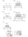
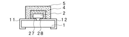
2 LEDチップ
3 接続手段
4 第1の樹脂層
4a 赤色変換部材
5 第2の樹脂層
5a 緑色変換部材
11 第1の電極膜
12 第2の電極膜
Claims (1)
- 両端部に一対の電極膜が形成される絶縁性基板と、該絶縁性基板上にマウントされる青色または紫外の光を発光する発光素子チップと、該発光素子チップの一対の電極を前記絶縁性基板に形成される一対の電極膜とそれぞれ電気的に接続される接続手段と、前記発光素子チップが発光する青色または紫外の光を赤色に変換する赤色変換部材が混入されたモールド樹脂からなり、前記発光素子チップおよび前記接続手段の部分を被覆するようにモールド成形された第1の樹脂層と、前記発光素子チップにより発光する青色または紫外の光を緑色に変換する緑色変換部材が混入されたモールド樹脂からなり、前記第1の樹脂層の周りを被覆するようにモールド成形された第2の樹脂層とを有し、前記発光素子チップに形成される一対の電極の1つが該チップの裏面側に形成されることにより、前記接続手段の一方は前記発光素子チップが前記一対の電極膜の一方の上にマウントされることによる接着剤であり、前記接続手段の他方は、前記発光素子チップの表面に設けられる電極と前記一対の電極膜の他方との間にワイヤボンディングされるワイヤであり、前記第1の樹脂層は、前記一対の電極膜の他方と接続されるワイヤの部分が厚く、前記一対の電極膜の一方の側が薄くなるように形成され、前記第2の樹脂層は前記ワイヤのある部分が薄く、前記一対の電極膜の一方の側が厚くなるように形成されてなる白色半導体発光素子。
Priority Applications (7)
| Application Number | Priority Date | Filing Date | Title |
|---|---|---|---|
| JP2005179659A JP4004514B2 (ja) | 2005-06-20 | 2005-06-20 | 白色半導体発光素子 |
| TW095121944A TW200739942A (en) | 2005-06-20 | 2006-06-19 | White semiconductor light emitting element and manufacturing method thereof |
| US11/922,508 US20090236622A1 (en) | 2005-06-20 | 2006-06-19 | White Semiconductor Light Emitting Device and Method for Manufacturing the Same |
| KR1020077029651A KR20080025687A (ko) | 2005-06-20 | 2006-06-19 | 백색 반도체 발광 소자 및 그 제법 |
| EP06766903A EP1895600A1 (en) | 2005-06-20 | 2006-06-19 | White semiconductor light emitting element and manufacturing method thereof |
| CN200680022297.5A CN101203964A (zh) | 2005-06-20 | 2006-06-19 | 白色半导体发光元件及其制造方法 |
| PCT/JP2006/312239 WO2006137359A1 (ja) | 2005-06-20 | 2006-06-19 | 白色半導体発光素子およびその製法 |
Applications Claiming Priority (1)
| Application Number | Priority Date | Filing Date | Title |
|---|---|---|---|
| JP2005179659A JP4004514B2 (ja) | 2005-06-20 | 2005-06-20 | 白色半導体発光素子 |
Publications (2)
| Publication Number | Publication Date |
|---|---|
| JP2006352037A JP2006352037A (ja) | 2006-12-28 |
| JP4004514B2 true JP4004514B2 (ja) | 2007-11-07 |
Family
ID=37647525
Family Applications (1)
| Application Number | Title | Priority Date | Filing Date |
|---|---|---|---|
| JP2005179659A Expired - Fee Related JP4004514B2 (ja) | 2005-06-20 | 2005-06-20 | 白色半導体発光素子 |
Country Status (2)
| Country | Link |
|---|---|
| JP (1) | JP4004514B2 (ja) |
| CN (1) | CN101203964A (ja) |
Families Citing this family (4)
| Publication number | Priority date | Publication date | Assignee | Title |
|---|---|---|---|---|
| JP2010267900A (ja) * | 2009-05-18 | 2010-11-25 | Citizen Holdings Co Ltd | Led光源装置の製造方法 |
| JPWO2013038649A1 (ja) * | 2011-09-13 | 2015-03-23 | 株式会社小糸製作所 | 発光モジュール |
| JP6326830B2 (ja) * | 2013-02-28 | 2018-05-23 | 日亜化学工業株式会社 | 発光装置及びそれを備える照明装置 |
| PL3534414T3 (pl) * | 2016-10-25 | 2024-04-08 | Seoul Semiconductor Co., Ltd. | Urządzenie wyświetlające oparte na pakietach diod elektroluminescencyjnych |
Family Cites Families (2)
| Publication number | Priority date | Publication date | Assignee | Title |
|---|---|---|---|---|
| JP3541709B2 (ja) * | 1998-02-17 | 2004-07-14 | 日亜化学工業株式会社 | 発光ダイオードの形成方法 |
| KR100691143B1 (ko) * | 2003-04-30 | 2007-03-09 | 삼성전기주식회사 | 다층 형광층을 가진 발광 다이오드 소자 |
-
2005
- 2005-06-20 JP JP2005179659A patent/JP4004514B2/ja not_active Expired - Fee Related
-
2006
- 2006-06-19 CN CN200680022297.5A patent/CN101203964A/zh active Pending
Also Published As
| Publication number | Publication date |
|---|---|
| CN101203964A (zh) | 2008-06-18 |
| JP2006352037A (ja) | 2006-12-28 |
Similar Documents
| Publication | Publication Date | Title |
|---|---|---|
| JP5634003B2 (ja) | 発光装置 | |
| US10777715B2 (en) | Semiconductor light emitting device | |
| JP5101650B2 (ja) | 半導体発光装置及びその製造方法 | |
| JP4254266B2 (ja) | 発光装置及び発光装置の製造方法 | |
| US6744196B1 (en) | Thin film LED | |
| WO2007102534A1 (ja) | チップ型半導体発光素子 | |
| WO2006137359A1 (ja) | 白色半導体発光素子およびその製法 | |
| JPH07288341A (ja) | Ledディスプレイ | |
| JP2009224538A (ja) | 半導体発光装置 | |
| JP2009059896A (ja) | 発光装置 | |
| JP2005209852A (ja) | 発光デバイス | |
| JP4773755B2 (ja) | チップ型半導体発光素子 | |
| JP2001298216A (ja) | 表面実装型の半導体発光装置 | |
| JP2001217461A (ja) | 複合発光素子 | |
| CN104576627B (zh) | 一种高显色性白光led结构及其制作方法 | |
| JP5983068B2 (ja) | 半導体発光素子及び発光装置 | |
| JP4004514B2 (ja) | 白色半導体発光素子 | |
| CN101673787B (zh) | 半导体发光装置及其封装结构 | |
| CN203607398U (zh) | 一种高显色性白光led结构 | |
| JP2006352036A (ja) | 白色半導体発光素子 | |
| JP3950898B2 (ja) | 白色半導体発光素子およびその製法 | |
| JP3509665B2 (ja) | 発光ダイオード | |
| KR20130007037A (ko) | 발광소자 패키지 및 그 제조 방법 | |
| JP2008041807A (ja) | 白色光源 | |
| JP6332503B2 (ja) | 発光装置及びその製造方法 |
Legal Events
| Date | Code | Title | Description |
|---|---|---|---|
| A521 | Request for written amendment filed |
Free format text: JAPANESE INTERMEDIATE CODE: A523 Effective date: 20061006 |
|
| A131 | Notification of reasons for refusal |
Free format text: JAPANESE INTERMEDIATE CODE: A131 Effective date: 20061128 |
|
| A521 | Request for written amendment filed |
Free format text: JAPANESE INTERMEDIATE CODE: A523 Effective date: 20070129 |
|
| A02 | Decision of refusal |
Free format text: JAPANESE INTERMEDIATE CODE: A02 Effective date: 20070417 |
|
| A521 | Request for written amendment filed |
Free format text: JAPANESE INTERMEDIATE CODE: A523 Effective date: 20070516 |
|
| A911 | Transfer to examiner for re-examination before appeal (zenchi) |
Free format text: JAPANESE INTERMEDIATE CODE: A911 Effective date: 20070621 |
|
| TRDD | Decision of grant or rejection written | ||
| A01 | Written decision to grant a patent or to grant a registration (utility model) |
Free format text: JAPANESE INTERMEDIATE CODE: A01 Effective date: 20070807 |
|
| A61 | First payment of annual fees (during grant procedure) |
Free format text: JAPANESE INTERMEDIATE CODE: A61 Effective date: 20070821 |
|
| R150 | Certificate of patent or registration of utility model |
Free format text: JAPANESE INTERMEDIATE CODE: R150 |
|
| FPAY | Renewal fee payment (event date is renewal date of database) |
Free format text: PAYMENT UNTIL: 20100831 Year of fee payment: 3 |
|
| FPAY | Renewal fee payment (event date is renewal date of database) |
Free format text: PAYMENT UNTIL: 20100831 Year of fee payment: 3 |
|
| FPAY | Renewal fee payment (event date is renewal date of database) |
Free format text: PAYMENT UNTIL: 20110831 Year of fee payment: 4 |
|
| LAPS | Cancellation because of no payment of annual fees |