JP4099672B2 - 半導体装置 - Google Patents
半導体装置 Download PDFInfo
- Publication number
- JP4099672B2 JP4099672B2 JP2004369587A JP2004369587A JP4099672B2 JP 4099672 B2 JP4099672 B2 JP 4099672B2 JP 2004369587 A JP2004369587 A JP 2004369587A JP 2004369587 A JP2004369587 A JP 2004369587A JP 4099672 B2 JP4099672 B2 JP 4099672B2
- Authority
- JP
- Japan
- Prior art keywords
- semiconductor device
- light shielding
- layer
- semiconductor
- shielding wall
- Prior art date
- Legal status (The legal status is an assumption and is not a legal conclusion. Google has not performed a legal analysis and makes no representation as to the accuracy of the status listed.)
- Expired - Lifetime
Links
Images


Classifications
-
- H—ELECTRICITY
- H10—SEMICONDUCTOR DEVICES; ELECTRIC SOLID-STATE DEVICES NOT OTHERWISE PROVIDED FOR
- H10F—INORGANIC SEMICONDUCTOR DEVICES SENSITIVE TO INFRARED RADIATION, LIGHT, ELECTROMAGNETIC RADIATION OF SHORTER WAVELENGTH OR CORPUSCULAR RADIATION
- H10F77/00—Constructional details of devices covered by this subclass
- H10F77/30—Coatings
- H10F77/306—Coatings for devices having potential barriers
- H10F77/331—Coatings for devices having potential barriers for filtering or shielding light, e.g. multicolour filters for photodetectors
- H10F77/334—Coatings for devices having potential barriers for filtering or shielding light, e.g. multicolour filters for photodetectors for shielding light, e.g. light blocking layers or cold shields for infrared detectors
-
- H—ELECTRICITY
- H10—SEMICONDUCTOR DEVICES; ELECTRIC SOLID-STATE DEVICES NOT OTHERWISE PROVIDED FOR
- H10B—ELECTRONIC MEMORY DEVICES
- H10B41/00—Electrically erasable-and-programmable ROM [EEPROM] devices comprising floating gates
- H10B41/30—Electrically erasable-and-programmable ROM [EEPROM] devices comprising floating gates characterised by the memory core region
-
- H—ELECTRICITY
- H10—SEMICONDUCTOR DEVICES; ELECTRIC SOLID-STATE DEVICES NOT OTHERWISE PROVIDED FOR
- H10B—ELECTRONIC MEMORY DEVICES
- H10B41/00—Electrically erasable-and-programmable ROM [EEPROM] devices comprising floating gates
- H10B41/60—Electrically erasable-and-programmable ROM [EEPROM] devices comprising floating gates the control gate being a doped region, e.g. single-poly memory cell
-
- H—ELECTRICITY
- H10—SEMICONDUCTOR DEVICES; ELECTRIC SOLID-STATE DEVICES NOT OTHERWISE PROVIDED FOR
- H10B—ELECTRONIC MEMORY DEVICES
- H10B69/00—Erasable-and-programmable ROM [EPROM] devices not provided for in groups H10B41/00 - H10B63/00, e.g. ultraviolet erasable-and-programmable ROM [UVEPROM] devices
-
- H—ELECTRICITY
- H10—SEMICONDUCTOR DEVICES; ELECTRIC SOLID-STATE DEVICES NOT OTHERWISE PROVIDED FOR
- H10W—GENERIC PACKAGES, INTERCONNECTIONS, CONNECTORS OR OTHER CONSTRUCTIONAL DETAILS OF DEVICES COVERED BY CLASS H10
- H10W42/00—Arrangements for protection of devices
- H10W42/20—Arrangements for protection of devices protecting against electromagnetic or particle radiation, e.g. light, X-rays, gamma-rays or electrons
Landscapes
- Internal Circuitry In Semiconductor Integrated Circuit Devices (AREA)
- Non-Volatile Memory (AREA)
- Semiconductor Memories (AREA)
Description
半導体層に設けられた半導体素子と、
前記半導体素子の周囲に設けられた遮光壁と、
前記遮光壁に設けられた開孔と、
前記半導体素子に電気的に接続された配線層であって、前記開孔から該遮光壁の外側に延伸された配線層と、を含み、
前記配線層は、前記開孔に位置している第1部分と、該開孔の外側に位置し該第1部分と比して大きい幅を有する第2部分と、を含むパターンを有し、
前記第2部分の幅は、前記開孔の幅と同一以上の幅である。
前記半導体素子の上方に設けられた層間絶縁層と、
前記層間絶縁層に設けられた溝と、
前記溝に埋め込まれた遮光材料と、を含むことができる。
フローティングゲート電極を有する不揮発性メモリであることができる。
第1の実施の形態の半導体装置について、図1、2を参照しつつ説明する。図1(A)は、本実施の形態にかかる半導体装置を模式的に示す平面図であり、図1(B)は、図1のA部を拡大して示す図であり、図2(A)は、図1(B)のI−I線に沿った断面図であり、図2(B)は、図1(B)のII−II線に沿った断面図であり、図2(C)は、図1(B)のIII−III線に沿った断面図である。
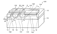
次に、第2の実施の形態について、図3〜図7を参照しつつ説明する。図3、4は、第2の実施の形態の半導体装置において、素子形成領域10Aに設けられる不揮発性メモリセル(以下、「メモリセル」という)を説明するための図であり、図5は、第2の実施の形態にかかる半導体装置を模式的に示す平面図であり、図6(A)は、図5のI−I線に沿った断面を模式的に示す断面図であり、図6(B)は、図5のII−II線に沿った断面図であり、図7は、第2の実施の形態の半導体装置の変形例を示す平面図である。
次に、第2の実施の形態の変形例にかかる半導体装置を、図7を参照しつつ説明する。図7は、変形例にかかる半導体装置を示す平面図であり、図5に対応する平面を示す。
次に、第3の実施の形態にかかる半導体装置について、図8、9を参照しつつ説明する。図8は、第3の実施の形態にかかる半導体装置を模式的に示す平面図であり、図5に対応した平面を示す図である。図9は、図8のA部を拡大して示す平面図である。図8に示すように、第3の実施の形態にかかる半導体装置は、上述の実施の形態にかかる半導体装置と比して第2部分26Bの形状が異なる例である。以下の説明では、上述の実施の形態と共通する構造については、詳細な説明は省略する。
図10は、第4の実施の形態にかかる半導体装置を模式的に示す平面図であり、図9に対応した平面を示す図である。図10に示すように、第4の実施の形態にかかる半導体装置は、上述の実施の形態にかかる半導体装置と比して第2部分の形状が異なる例である。以下の説明では、上述の実施の形態と共通する構造については、詳細な説明は省略する。
図11は、第5の実施の形態にかかる半導体装置を模式的に示す平面図であり、図9に対応した平面を示す図である。図11に示すように、第5の実施の形態にかかる半導体装置は、上述の実施の形態にかかる半導体装置と比して第2部分の形状が異なる例である。以下の説明では、上述の実施の形態と共通する構造については、詳細な説明は省略する。
Claims (16)
- 半導体素子と、
前記半導体素子の周囲に設けられ、開孔を有する遮光壁と、
前記半導体素子に電気的に接続された配線層であって、前記開孔から前記遮光壁の外側に延伸された配線層と、を含み、
前記配線層は、前記開孔に位置している第1部分と、前記遮光壁に囲まれた領域以外に位置し該第1部分と比して大きい幅を有する第2部分と、を含むパターンを有し、
前記第2部分は、前記開孔の幅と同一以上の幅を有する、半導体装置。 - 請求項1において、
前記第1部分が延伸している方向からみたときに、前記第2部分は、少なくとも前記開孔と重なるように設けられている、半導体装置。 - 請求項1または2において、
前記第2部分は、前記第1部分が延伸した方向を軸として該軸と交差する方向に分岐した分岐部を含む、半導体装置。 - 請求項1または2において、
前記第2部分は、前記第1部分が延伸した方向を軸として該軸と直角の方向に延在している、半導体装置。 - 請求項1ないし4のいずれかにおいて、
前記第2部分は、前記半導体素子の位置を前記遮光壁の内側とした場合、前記遮光壁に囲まれた領域の外側に設けられている、半導体装置。 - 請求項1ないし5のいずれかにおいて、
さらに、前記半導体素子の上方に設けられた遮光膜を含む、半導体装置。 - 請求項1ないし6のいずれかにおいて、
前記遮光壁は、
前記半導体素子の上方に設けられた層間絶縁層と、
前記層間絶縁層に設けられた溝と、
前記溝に埋め込まれた遮光材料と、を含む、半導体装置。 - 請求項1ないし7のいずれかにおいて、
前記半導体素子は、
フローティングゲート電極を有する不揮発性メモリである、半導体装置。 - 請求項8において、
前記不揮発性メモリは、単層ゲート型の不揮発性メモリである、半導体装置。 - 請求項1ないし9のいずれかにおいて、
前記配線層は、信号線である、半導体装置。 - 請求項1ないし10のいずれかにおいて、
さらに、半導体層を含み、
前記配線層は、前記半導体層の上方に設けられている、半導体装置。 - 請求項1ないし11のいずれかにおいて、
前記半導体素子は、トランジスタである、半導体装置。 - 請求項1ないし12のいずれかにおいて、
前記第2部分の幅は、前記遮光壁の一辺よりも小さい、半導体装置。 - 請求項7において、
前記遮光材料は、導電層である、半導体装置。 - 請求項14において、
前記導電層は、金属層である、半導体装置。 - 請求項1ないし15のいずれかにおいて、
前記第2部分によって、前記開孔から前記遮光壁に囲まれた領域への光の進入が低減されている、半導体装置。
Priority Applications (5)
| Application Number | Priority Date | Filing Date | Title |
|---|---|---|---|
| JP2004369587A JP4099672B2 (ja) | 2004-12-21 | 2004-12-21 | 半導体装置 |
| US11/249,253 US7253462B2 (en) | 2004-12-21 | 2005-10-13 | Semiconductor device |
| US11/768,514 US7482647B2 (en) | 2004-12-21 | 2007-06-26 | Semiconductor device |
| US11/768,589 US7508019B2 (en) | 2004-12-21 | 2007-06-26 | Semiconductor device |
| US11/768,387 US7612396B2 (en) | 2004-12-21 | 2007-06-26 | Semiconductor device |
Applications Claiming Priority (1)
| Application Number | Priority Date | Filing Date | Title |
|---|---|---|---|
| JP2004369587A JP4099672B2 (ja) | 2004-12-21 | 2004-12-21 | 半導体装置 |
Related Child Applications (3)
| Application Number | Title | Priority Date | Filing Date |
|---|---|---|---|
| JP2008016012A Division JP4766277B2 (ja) | 2008-01-28 | 2008-01-28 | 半導体装置 |
| JP2008016011A Division JP4735863B2 (ja) | 2008-01-28 | 2008-01-28 | 半導体装置 |
| JP2008016013A Division JP4735864B2 (ja) | 2008-01-28 | 2008-01-28 | 半導体装置 |
Publications (2)
| Publication Number | Publication Date |
|---|---|
| JP2006179590A JP2006179590A (ja) | 2006-07-06 |
| JP4099672B2 true JP4099672B2 (ja) | 2008-06-11 |
Family
ID=36594574
Family Applications (1)
| Application Number | Title | Priority Date | Filing Date |
|---|---|---|---|
| JP2004369587A Expired - Lifetime JP4099672B2 (ja) | 2004-12-21 | 2004-12-21 | 半導体装置 |
Country Status (2)
| Country | Link |
|---|---|
| US (4) | US7253462B2 (ja) |
| JP (1) | JP4099672B2 (ja) |
Cited By (1)
| Publication number | Priority date | Publication date | Assignee | Title |
|---|---|---|---|---|
| JP2006295046A (ja) * | 2005-04-14 | 2006-10-26 | Seiko Epson Corp | 半導体装置 |
Families Citing this family (7)
| Publication number | Priority date | Publication date | Assignee | Title |
|---|---|---|---|---|
| JP4626373B2 (ja) * | 2005-04-14 | 2011-02-09 | セイコーエプソン株式会社 | 半導体装置 |
| KR101427581B1 (ko) * | 2007-11-09 | 2014-08-07 | 삼성디스플레이 주식회사 | 유기 발광 표시 장치 및 그 제조 방법 |
| JP4766277B2 (ja) * | 2008-01-28 | 2011-09-07 | セイコーエプソン株式会社 | 半導体装置 |
| JP4735863B2 (ja) * | 2008-01-28 | 2011-07-27 | セイコーエプソン株式会社 | 半導体装置 |
| JP4735864B2 (ja) * | 2008-01-28 | 2011-07-27 | セイコーエプソン株式会社 | 半導体装置 |
| US8708697B2 (en) | 2009-12-08 | 2014-04-29 | Align Technology, Inc. | Tactile objects for orthodontics, systems and methods |
| US7999361B1 (en) * | 2010-02-19 | 2011-08-16 | Altera Corporation | Shielding structure for transmission lines |
Family Cites Families (22)
| Publication number | Priority date | Publication date | Assignee | Title |
|---|---|---|---|---|
| JPS61129875A (ja) | 1984-11-28 | 1986-06-17 | Seiko Epson Corp | 半導体装置 |
| JPS63308388A (ja) | 1987-06-10 | 1988-12-15 | Mitsubishi Electric Corp | 半導体記憶装置 |
| JPS63310180A (ja) | 1987-06-11 | 1988-12-19 | Mitsubishi Electric Corp | 半導体メモリ装置 |
| JPH01117375A (ja) * | 1987-10-30 | 1989-05-10 | Hamamatsu Photonics Kk | 半導体装置 |
| JPH04321273A (ja) * | 1991-04-19 | 1992-11-11 | Fuji Xerox Co Ltd | イメージセンサ |
| US5525827A (en) * | 1993-11-05 | 1996-06-11 | Norman; Kevin A. | Unerasable electronic programmable read only memory (UPROM™) |
| US5736756A (en) * | 1994-09-29 | 1998-04-07 | Sony Corporation | Solid-state image sensing device with lght shielding film |
| US6266110B1 (en) * | 1996-07-30 | 2001-07-24 | Kawasaki Steel Corporation | Semiconductor device reeventing light from entering its substrate transistor and the same for driving reflection type liquid crystal |
| JP3716580B2 (ja) * | 1997-02-27 | 2005-11-16 | セイコーエプソン株式会社 | 液晶装置及びその製造方法、並びに投写型表示装置 |
| JPH1113979A (ja) * | 1997-06-26 | 1999-01-22 | Kitz Corp | 電気融着継手とその固定方法 |
| US6166403A (en) * | 1997-11-12 | 2000-12-26 | Lsi Logic Corporation | Integrated circuit having embedded memory with electromagnetic shield |
| JP3601761B2 (ja) * | 1998-11-19 | 2004-12-15 | 松下電器産業株式会社 | 受光素子およびその製造方法 |
| JP4700156B2 (ja) * | 1999-09-27 | 2011-06-15 | 株式会社半導体エネルギー研究所 | 半導体装置 |
| JP3478768B2 (ja) * | 1999-10-04 | 2003-12-15 | 三洋電機株式会社 | 半導体装置 |
| JP2001354968A (ja) * | 2000-06-09 | 2001-12-25 | Hitachi Ltd | アクティブ・マトリクス型液晶表示装置およびその液晶組成物質 |
| US6653617B2 (en) * | 2000-07-03 | 2003-11-25 | Canon Kabushiki Kaisha | Photoelectric conversion device |
| JP2003124363A (ja) | 2001-10-19 | 2003-04-25 | Toshiba Corp | 半導体記憶装置 |
| JP3928543B2 (ja) * | 2001-12-11 | 2007-06-13 | セイコーエプソン株式会社 | 電機光学装置用基板及びその製造方法、電気光学装置並びに電子機器 |
| US6956281B2 (en) * | 2002-08-21 | 2005-10-18 | Freescale Semiconductor, Inc. | Semiconductor device for reducing photovolatic current |
| JP2004104203A (ja) * | 2002-09-05 | 2004-04-02 | Toshiba Corp | 固体撮像装置 |
| JP3794411B2 (ja) * | 2003-03-14 | 2006-07-05 | セイコーエプソン株式会社 | 表示装置および電子機器 |
| JP4274118B2 (ja) * | 2004-12-27 | 2009-06-03 | セイコーエプソン株式会社 | 半導体装置 |
-
2004
- 2004-12-21 JP JP2004369587A patent/JP4099672B2/ja not_active Expired - Lifetime
-
2005
- 2005-10-13 US US11/249,253 patent/US7253462B2/en not_active Expired - Lifetime
-
2007
- 2007-06-26 US US11/768,514 patent/US7482647B2/en not_active Expired - Fee Related
- 2007-06-26 US US11/768,589 patent/US7508019B2/en not_active Expired - Fee Related
- 2007-06-26 US US11/768,387 patent/US7612396B2/en not_active Expired - Fee Related
Cited By (1)
| Publication number | Priority date | Publication date | Assignee | Title |
|---|---|---|---|---|
| JP2006295046A (ja) * | 2005-04-14 | 2006-10-26 | Seiko Epson Corp | 半導体装置 |
Also Published As
| Publication number | Publication date |
|---|---|
| US20070246758A1 (en) | 2007-10-25 |
| US7482647B2 (en) | 2009-01-27 |
| JP2006179590A (ja) | 2006-07-06 |
| US20060131626A1 (en) | 2006-06-22 |
| US7612396B2 (en) | 2009-11-03 |
| US20070246759A1 (en) | 2007-10-25 |
| US7253462B2 (en) | 2007-08-07 |
| US20070246760A1 (en) | 2007-10-25 |
| US7508019B2 (en) | 2009-03-24 |
Similar Documents
| Publication | Publication Date | Title |
|---|---|---|
| CN107393924A (zh) | 具有辅助栅极的非易失性存储单元结构及其存储器数组 | |
| US7612396B2 (en) | Semiconductor device | |
| US7667249B2 (en) | Semiconductor device | |
| US20080012141A1 (en) | Semiconductor device | |
| JP4274118B2 (ja) | 半導体装置 | |
| JP4735862B2 (ja) | 半導体装置 | |
| JP4735864B2 (ja) | 半導体装置 | |
| JP4735863B2 (ja) | 半導体装置 | |
| JP4766277B2 (ja) | 半導体装置 | |
| JP5029844B2 (ja) | 半導体装置 | |
| JP4858671B2 (ja) | 半導体装置 | |
| JP4952954B2 (ja) | 半導体装置 | |
| US6818942B2 (en) | Non-volatile semiconductor storage device having conductive layer surrounding floating gate | |
| KR100486238B1 (ko) | 노어형 플래쉬 메모리소자의 셀 어레이부 | |
| JP2006216683A (ja) | 半導体装置 |
Legal Events
| Date | Code | Title | Description |
|---|---|---|---|
| A977 | Report on retrieval |
Free format text: JAPANESE INTERMEDIATE CODE: A971007 Effective date: 20071126 |
|
| A131 | Notification of reasons for refusal |
Free format text: JAPANESE INTERMEDIATE CODE: A131 Effective date: 20071128 |
|
| A521 | Request for written amendment filed |
Free format text: JAPANESE INTERMEDIATE CODE: A523 Effective date: 20080128 |
|
| TRDD | Decision of grant or rejection written | ||
| A01 | Written decision to grant a patent or to grant a registration (utility model) |
Free format text: JAPANESE INTERMEDIATE CODE: A01 Effective date: 20080220 |
|
| A61 | First payment of annual fees (during grant procedure) |
Free format text: JAPANESE INTERMEDIATE CODE: A61 Effective date: 20080304 |
|
| FPAY | Renewal fee payment (event date is renewal date of database) |
Free format text: PAYMENT UNTIL: 20110328 Year of fee payment: 3 |
|
| R150 | Certificate of patent or registration of utility model |
Ref document number: 4099672 Country of ref document: JP Free format text: JAPANESE INTERMEDIATE CODE: R150 Free format text: JAPANESE INTERMEDIATE CODE: R150 |
|
| FPAY | Renewal fee payment (event date is renewal date of database) |
Free format text: PAYMENT UNTIL: 20120328 Year of fee payment: 4 |
|
| FPAY | Renewal fee payment (event date is renewal date of database) |
Free format text: PAYMENT UNTIL: 20120328 Year of fee payment: 4 |
|
| FPAY | Renewal fee payment (event date is renewal date of database) |
Free format text: PAYMENT UNTIL: 20130328 Year of fee payment: 5 |
|
| FPAY | Renewal fee payment (event date is renewal date of database) |
Free format text: PAYMENT UNTIL: 20140328 Year of fee payment: 6 |
|
| S531 | Written request for registration of change of domicile |
Free format text: JAPANESE INTERMEDIATE CODE: R313531 |
|
| R350 | Written notification of registration of transfer |
Free format text: JAPANESE INTERMEDIATE CODE: R350 |