JP4105809B2 - Appearance inspection method and appearance inspection apparatus - Google Patents
Appearance inspection method and appearance inspection apparatus Download PDFInfo
- Publication number
- JP4105809B2 JP4105809B2 JP25393498A JP25393498A JP4105809B2 JP 4105809 B2 JP4105809 B2 JP 4105809B2 JP 25393498 A JP25393498 A JP 25393498A JP 25393498 A JP25393498 A JP 25393498A JP 4105809 B2 JP4105809 B2 JP 4105809B2
- Authority
- JP
- Japan
- Prior art keywords
- defect
- detection
- optical system
- image
- condition
- Prior art date
- Legal status (The legal status is an assumption and is not a legal conclusion. Google has not performed a legal analysis and makes no representation as to the accuracy of the status listed.)
- Expired - Fee Related
Links
Images




Landscapes
- Investigating Materials By The Use Of Optical Means Adapted For Particular Applications (AREA)
- Preparing Plates And Mask In Photomechanical Process (AREA)
- Testing Or Measuring Of Semiconductors Or The Like (AREA)
- Image Processing (AREA)
- Image Analysis (AREA)
- Length Measuring Devices With Unspecified Measuring Means (AREA)
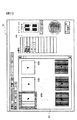
Description
【0001】
【発明の属する技術分野】
本発明は、半導体ウェーハ、フォトマスク、磁気ディスク等を検査対象とする外観検査方法および外観検査装置に係り、特に、検査対象に対して本来同一であるべきパターン等を検出して、パターン異常や異物付着などの欠陥を検査すると共に、欠陥の解析を行って分類分けを必要とするものに用いて好適な、外観検査技術に関する。
【0002】
【従来の技術】
従来、この種類の外観検査技術としては、図5〜図7に示す方式のものが知られている。
【0003】
図5に示した構成は、設計データ比較方式と呼ばれるものである。図5に示すように、XYステージ1上に設置されたZθステージ2上には、被検査物(試料)である半導体ウェーハ3が載置されている。この半導体ウェーハ3の上方には、照明光源4からの照明光を、半導体ウェーハ3側へ向けるハーフミラー6が設けてあり、このハーフミラー6で反射された照明光は、対物レンズ5を経て、半導体ウェーハ3を照明する。半導体ウェーハ3からの反射光は、対物レンズ5、ハーフミラー6を経て、検出光として検出器(例えば、CCDイメージセンサ)7で受光される。
【0004】
そして、検出器7で受光された検出光は、A/Dコンバータ8によってデジタル画像信号に変換され、設計データパターン発生回路9によって生成されるデータと、信号比較手段10にて比較が行われる。このとき、両者の信号に不一致となる個所があった場合には、欠陥があると判定される。
【0005】
図6に示した構成は、2眼2チップ比較方式と呼ばれるものであり、同図において、先に説明したものと均等な(同等の機能を有する)構成要素には同一符号を付してある(これは、以下の説明においても同様である)。
【0006】
この2眼2チップ比較方式は、図5で述べた照明から検出までの一連の光学系を2組持ち、双方の検出器7、7で受光された信号は、A/Dコンバータ8、8によってそれぞれデジタル画像信号に変換された後に、信号比較手段10にて比較され、欠陥判定が行われる。
【0007】
図7に示した構成は、1眼2チップ比較方式と呼ばれるものである。この方式は、図5で述べた照明から検出までの一連の光学系を持ち、最初の走査領域で検出した検出信号を画像記憶回路11に記憶させた後に、この記憶させた検出信号と次の走査領域で得られる検出信号とを、信号比較手段10で比較して、検出信号の一致/不一致を検出し、欠陥判定が行われる。
【0008】
上述した3つの方式は、何れの場合も、検査を高速に行うために連続的なステージの走査により2次元画像を検出する方式を採用しており、いわゆるステップ&リピートの方式で画像を検出する方式は採用されていない。
【0009】
また、上述したような外観検査の結果の分類や、解析シーケンスとしては、図8あるいは図9に示す方式のものが知られている。
【0010】
図8は、人の目視確認による分類のシーケンスである。まず、外観検査装置によって検査を行い、得られた欠陥の座標情報をもとに、装置上で各欠陥部の画像表示を行う。一般的には、検査時の処理画像の解像度を上回る解像度でこの表示を行う。次に、人がこの画像を目で見て、欠陥の色、形状、背景の情報をもとに、欠陥のカテゴリ分類を行う。
【0011】
図9は、自動欠陥分類機能の導入による分類シーケンスである。まず、外観検査装置によって検査を行い、得られた欠陥の座標情報をもとに、装置上で各欠陥部の画像検出を行う。自動分類においても、検査時の処理画像の解像度を上回る解像度でこの検出を行う。次に、自動分類機能により、画像から欠陥の色、形状、背景、座標の情報をもとに、欠陥のカテゴリ分類を行う。自動分類機能の導入により、目視確認時と比べて、欠陥レビュー効率の向上と分類の規格化が図られている。
【0012】
【発明が解決しようとする課題】
ところで、上述した従来技術においては、下記のような問題がある。
前記した図5〜図7の検査方式と、前記した図8、図9の分類、解析シーケンスとの組み合わせに共通しているのは、欠陥の有無の検査時には、実用的な検査時間確保のため低倍率で検査画像の検出を行い、この検査終了後に分類、解析を行うため、検査結果による欠陥座標情報に基づいて、高倍率で欠陥部の画像の再検出を行っている点である。このように欠陥部の画像を再検出する所以は、検査効率向上のため検査装置がステージ走査により画像検出を行っているため、一度のステージ走査で異なる倍率の画像を検出することが困難であるためであり、これが、欠陥の分類分けを含めた総検査時間を増加させる要因となっている。
【0013】
例えば、半導体ウェーハの外観検査における例では、被検査物1枚あたりの欠陥検査時間(欠陥の検出時間)が約15分である。これに対して分類処理は、検査結果に対して間引きを行い100点程度の欠陥を対象に行う。自動分類に要する時間が3秒/点とした場合、被検査物1枚あたりの分類処理で、300秒(5分)の時間を要することになり、実に欠陥検査時間の1/3を占めることになる。この間、被検査物であるウェーハは検査装置上に拘束されて、次のプロセスに進むことはできない。
【0014】
上記の分類のための欠陥部の画像の再検出は、検査時に比べて画素寸法にして2倍〜8倍程度の高解像度な画像を必要とするために行っている。このため、検査時の処理画像を用いた場合には、十分な精度の欠陥分類は困難である。逆に、検査画素寸法を分類用の画像検出時と同じにした場合には、検査処理を行う画素数は16倍〜64倍となるため、装置の回路規模と検査時間の大幅な増大を招き、実用的ではなくなる。
【0015】
近年、ウェーハの大径化が進んでおり、φ200からφ300へと移行しようとしている。このため、ウェーハ1枚あたりの分類対象数が増加することは明らかであり、従来技術による検査方式では、分類対象数の増加分の時間が増加するという問題をはらんでいる。
【0016】
本発明は、上記した課題に着目してなされたものであり、その目的とするところは、外観検査における欠陥分類時間を短縮することのできる技術を提供することある。
【0017】
【課題を解決するための手段】
試料を相対的に走査しながら第1の検出光学系を用いて第1の検出条件で得られる検出信号を処理して欠陥を検知し該検知した欠陥の特徴量の情報と位置情報とを得、上記試料を相対的に走査しながら第2の検出光学系を用いて上記第1の検出条件とは異なる第2の検出条件で得られる検出信号を処理して得られる画像データを記憶し、該記憶した画像データの中から前記第1の検出光学系を用いて検出した欠陥の位置情報に対応する位置の欠陥の画像を抽出し、該抽出した欠陥の画像を該欠陥の位置情報及び特徴量の情報と共に画面上に表示する。
【0018】
【発明の実施の形態】
以下、本発明の実施の形態を説明する。
図1は、本発明の第1実施形態に係る外観検査装置の構成を示す図である。図1に示すように、XYステージ1上に設置されたZθステージ2上には、被検査物(試料)である半導体ウェーハ3が載置されている。この半導体ウェーハ3の上方には、照明光源4からの照明光を半導体ウェーハ3側へ向けるハーフミラー6が設けてあり、このハーフミラー6で反射された照明光は、対物レンズ5を経て、半導体ウェーハ3を照明する。
【0019】
半導体ウェーハ3からの反射光は、対物レンズ5、ハーフミラー6を経て、ハーフミラー6Aで透過して、低倍率検出系20において、検出光として検出器(CCDイメージセンサ)7Aで受光されるものと、ハーフミラー6Aで反射したのちに、高倍率検出系21において、ズームレンズ22を経て検出光として検出器(CCDイメージセンサ)7Bで受光されるものとに、別れる構成となっている。なお、低倍率検出系20は、欠陥検出の精度保証には充分な倍率であるも、高倍率検出系21よりも低解像度の検出光学系となっており、高倍率検出系21は、低倍率検出系20よりも高解像度である(例えば、低倍率検出系20よりも2倍〜8倍程度高解像度である)、高解像度の検出光学系となっている。
【0020】
ここで、上記の低倍率検出系20および高倍率検出系21にて、同時に画像の検出を行うためには、検出器7Aによる検出画素寸法P1、検出器7Bによる検出画素寸法P2、検出器7Aのステージ進行方向の1ラインあたりの走査時間T1、検出器7Bのステージ進行方向の1ラインあたり走査時間T2、ステージ移動速度V、ズームレンズ22の倍率Zの間に、次式の関係が成立している必要がある。
V=P1/T1=P2/T1
P2=Z×P1
実用上は、P1、P2およびT1から、上式を満たすT2を算出すると、実現が困難な高速な検出器を要求することになるが、検出器7Bをマルチチャンネル化して、チャンネル毎の画素の読み出し時間を稼ぐことで対応可能である。
【0021】
検出器7Aで受光された検出光は、A/Dコンバータ8によってデジタルの画像信号に変換され、欠陥検出部23に入力される。欠陥検出部23では、A/Dコンバータ8からの入力データと、これと比較するためのデータとの対比を行って、欠陥の有無の判定を行う。すなわち図1では割愛してあるが、欠陥検出部23は、例えば、前記図5の構成と同様に、設計データに基づき設計データパターン発生回路によって生成されるデータと、A/Dコンバータ8からの入力データとを比較するか、あるいは、前記図7の構成と同様に、前の走査領域で取り込んで画像記憶回路に記憶させたデータと、A/Dコンバータ8からの入力データとを比較することによって、欠陥判定を行う。そして、欠陥が見出された場合には、欠陥検出部23は、欠陥の寸法、面積、形状、色、背景などの特徴量を表わす欠陥情報24と、欠陥の座標情報25とを出力する。欠陥画像データベース26では、欠陥検出部23が出力した欠陥情報24と座標情報25を保管する。
【0022】
一方、検出器7Bにおいて高倍率の検出光から得られた検出信号は、A/Dコンバータ8によってデジタルの画像信号に変換され、一時メモリとしての遅延メモリ27に送られて、高倍率(高解像度)の画像データとして格納される。遅延メモリ読み出し回路28は、欠陥検出部23が出力する欠陥の座標情報25を受けて、遅延メモリ27上の対応する画像データを欠陥部を中心として抽出して、これを画像メモリ29に転送して一旦格納させる。なお、遅延メモリ27は、欠陥部の画像データを所定のタイムラグをもって抽出するために、十分な容量を持つものとして構成されている。ただし、遅延メモリ27は試料の全領域の画像データを保持する必要は全くなく、上記した所定のタイムラグをもった画像データの抽出を保証すればよいもので、さほど大規模な容量をもつものとして構成する必要はない。
【0023】
画像メモリ29に格納された欠陥部の画像データ(欠陥画像)は、欠陥情報編集用コンピュータ30によって、欠陥画像データベース26に格納された欠陥情報24、座標情報25と対応付けて、欠陥画像データベース31に保管される。そして、欠陥画像の閲覧、検索時には、欠陥画像データベース31に格納された内容は、欠陥情報編集用コンピュータ30によって適宜に読み出されて、欠陥部の画像データ(欠陥画像)に、欠陥情報、座標情報を付加して、CRT32に出力して表示されるようになっている。
【0024】
上記のように、欠陥画像データベース31に保管された欠陥画像、欠陥情報、座標情報は、欠陥情報編集用コンピュータ30によってCRT32上に表示され、これを用いて、オペレーターが欠陥の分類分けを行うことができるようになっており、この目視分類分けしたデータも、欠陥画像データベース31に、欠陥画像、欠陥情報、座標情報と対応付けて格納されるようになっている。また、欠陥画像データベース31に格納された内容は、欠陥情報編集用コンピュータ30によって、CRT32上で閲覧、検索ができることは勿論、拡大、縮小、移動、重ね合わせ、色替えなどの各種表示処理や、データの並べ替え、転送、複写、削除などの各種編集処理が可能となっている。
【0025】
図2は、本実施形態において、CRT32上に表示される欠陥の目視分類用の操作画面の1例を示す図である。図2に示した例では、表示画面41における、品種名、工程、ウェーハ、検査日時の表示欄の下に、欠陥画像を縮小した一覧表示欄42を設け、この一覧表示欄42内をスクロール操作することによって、各欠陥画像(各欠陥部の画像データ)43a、43b、43c……を視認できるようにしている。そして、オペレーターは分類指定を行う欠陥画像を指定し、また必要に応じてこの指定した縮小欠陥画像を拡大表示して、これによって、オペレーターは選択画像に対して分類の指定を順次行って、この分類指定を分類名入力欄44に順次書き込むことにより、オペレータによる欠陥の目視分類処理が行われるようになっている。ここで、CRT32上に表示される欠陥画像は、先にも述べたように、高倍率の画像データ、換言するなら高解像度の画像データであるので、表示は鮮明でかつ詳細なものとなっていることは言うまでもない。
【0026】
なお、欠陥画像データベース31に保管された欠陥画像、欠陥情報、座標情報、分類分け情報などのデータは、ネットワーク、あるいはMOドライブ等の大容量メディアにより、外部機器に対しデータの転送を行うことで、オフラインレビューや、あるいは、自動欠陥分類装置への接続も可能となっている。
【0027】
図3は、本発明の第2実施形態に係る外観検査装置の構成を示す図である。図3に示すように、XYステージ1上に設置されたZθステージ2上には、被検査物(試料)である半導体ウェーハ3が載置されている。この半導体ウェーハ3の上方には、2つの光学系、すなわち、欠陥検出の精度保証には充分な倍率であるも、比較的に低解像度の検出光学系である低倍率検出系20Aと、この低倍率検出系20Aよりも高解像度である(例えば、低倍率検出系20Aよりも2倍〜8倍程度高解像度である)、高解像度の検出光学系である高倍率検出系21Aとが設けてある。
【0028】
低倍率検出系20Aおよび高倍率検出系21Aには、それぞれの照明光源4、4からの照明光を半導体ウェーハ3側へ向けるハーフミラー6、6が設けてあり、このハーフミラー6、6で反射された照明光は、それぞれ対物レンズ5、5を経て、半導体ウェーハ3を照明する。
【0029】
低倍率検出系20Aでは、半導体ウェーハ3からの反射光は、対物レンズ5、ハーフミラー6を経て、検出光として検出器7Aで受光され、A/Dコンバータ8によってデジタルの画像信号に変換され、欠陥検出部23に入力される。欠陥検出部23では、A/Dコンバータ8からの入力データと、これと比較するためのデータとの対比を行って、欠陥の有無の判定を行う。すなわち図3では割愛してあるが、欠陥検出部23は、例えば、前記図5の構成と同様に、設計データに基づき設計データパターン発生回路によって生成されるデータと、A/Dコンバータ8からの入力データとを比較するか、あるいは、前記図7の構成と同様に、前の走査領域で取り込んで画像記憶回路に記憶させたデータと、A/Dコンバータ8からの入力データとを比較することによって、欠陥判定を行う。そして、欠陥が見出された場合には、欠陥検出部23は、欠陥の寸法、面積、形状、色、背景などの特徴量を表わす欠陥情報24と、欠陥の座標情報25とを出力する。欠陥画像データベース26では、欠陥検出部23が出力した欠陥情報24と座標情報25を保管する。
【0030】
一方、高倍率検出系21Aでは、半導体ウェーハ3からの反射光は、対物レンズ5、ハーフミラー6、ズームレンズ22を経て、高倍率の検出光として検出器7Bで受光される。検出器7Bにおいて高倍率の検出光から得られた検出信号は、A/Dコンバータ8によってデジタルの画像信号に変換され、一時メモリとしての遅延メモリ27に送られて、高倍率(高解像度)の画像データとして格納される。遅延メモリ読み出し回路28は、欠陥検出部23が出力する欠陥の座標情報25を受けて、遅延メモリ27上の対応する画像データを欠陥部を中心として抽出して、これを画像メモリ29に転送して一旦格納させる。なお、遅延メモリ27は、欠陥部の画像データを所定のタイムラグをもって抽出するために、十分な容量を持つものとして構成されている。
【0031】
本実施形態においても、低倍率検出系20Aおよび高倍率検出系21Aにて、同時に画像の検出を行うためには、検出器7Aによる検出画素寸法P1、検出器7Bによる検出画素寸法P2、検出器7Aのステージ進行方向の1ラインあたりの走査時間T1、検出器7Bのステージ進行方向の1ラインあたり走査時間T2、ステージ移動速度V、ズームレンズ22の倍率Zの間に、次式の関係が成立している必要がある。
V=P1/T1=P2/T1
P2=Z×P1
実用上は、P1、P2およびT1から、上式を満たすT2を算出すると、実現が困難な高速な検出器を要求することになるが、検出器7Bをマルチチャンネル化して、チャンネル毎の画素の読み出し時間を稼ぐことで対応可能である。
【0032】
ただし、本実施形態においては、前記第1実施形態と異なり、2つの検出系の距離分は、ステージを余分に走査する必要があり、検査時間の増加を招くが、独立した2つの検出系を持っているため、1系統の検出系では実現が困難である、照明波長領域、焦点位置、偏光などの異なる2つ光学条件の実現や、高倍率(高解像度)検出系21Aとして、SEM(走査型電子顕微鏡)を用いることも可能になるという特徴がある。
【0033】
上述のようにして、画像メモリ29に格納された欠陥部の画像データ(欠陥画像)は、欠陥情報編集用コンピュータ30によって、欠陥画像データベース26に格納された欠陥情報24、座標情報25と対応付けて、欠陥画像データベース31に保管される。そして、欠陥画像の閲覧、検索時には、欠陥画像データベース31に格納された内容は、欠陥情報編集用コンピュータ30によって適宜に読み出されて、欠陥部の画像データ(欠陥画像)に、欠陥情報、座標情報を付加して、CRT32に出力して表示されるようになっている。
【0034】
そして、欠陥画像データベース31に保管された欠陥画像、欠陥情報、座標情報は、前記した第1実施形態と同様に、欠陥情報編集用コンピュータ30によってCRT32上に表示され、これを用いて、オペレーターが欠陥の分類分けを行うことができるようになっており、この目視分類分けしたデータも、欠陥画像データベース31に、欠陥画像、欠陥情報、座標情報と対応付けて格納されるようになっている。また、欠陥画像データベース31に格納された内容は、欠陥情報編集用コンピュータ30によって、CRT32上で閲覧、検索ができることは勿論、拡大、縮小、移動、重ね合わせ、色替えなどの各種表示処理や、データの並べ替え、転送、複写、削除などの各種編集処理が可能となっている。なおまた、欠陥画像データベース31に保管された欠陥画像、欠陥情報、座標情報、分類分け情報などのデータは、ネットワーク、あるいはMOドライブ等の大容量メディアにより、外部機器に対しデータの転送を行うことで、オフラインレビューや、自動欠陥分類装置への接続も可能となっている。
【0035】
なお、上述した第1、第2実施形態において、低倍率検出系をグレースケールの画像データを得る検出系とし、高倍率検出系をカラー画像データを得る検出系としてもよい。何となれば、欠陥検出は明るさの情報があれば可能であり、こうすることにより、低倍率検出系の構成が簡単化されてコスト低減が可能となり、また、オペレータの目視による欠陥の分類分け、または自動欠陥分類分けには、色情報があった方がより詳細で確実な判断が下せるからである。なおまた、第2実施形態においては、先にも述べたように、高倍率検出系として、SEM(走査型電子顕微鏡)を用いることも可能で、こうすることによって、より高解像度の欠陥部画像データを得ることが可能となる。
【0036】
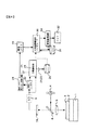
図4は、本発明の第3実施形態に係る外観検査装置の構成を示す図である。図4に示すように、XYステージ1上に設置されたZθステージ2上には、被検査物(試料)である半導体ウェーハ3が載置されている。この半導体ウェーハ3の上方には、照明光源4からの照明光を半導体ウェーハ3側へ向けるハーフミラー6が設けてあり、このハーフミラー6で反射された照明光は、対物レンズ5を経て、半導体ウェーハ3を照明する。
【0037】
半導体ウェーハ3からの反射光は、対物レンズ5、ハーフミラー6を経て、検出光として検出器7Aで受光される(なお、本実施形態の検出光学系は、前記第2実施形態の低倍率検出系20Aに相当するものとなっている)。検出器7Aで受光された検出光は、A/Dコンバータ8によってデジタル画像信号に変換され、遅延メモリ33および欠陥判定部23に入力される。欠陥判定部23は、前記図7の構成と同様に、前の走査領域で取り込んで遅延メモリ33に記憶させたデータと、A/Dコンバータ8からの入力データとを比較することによって、欠陥判定を行う。そして、欠陥が見出された場合には、欠陥検出部23は、欠陥の寸法、面積、形状、色、背景などの特徴量を表わす欠陥情報24と、欠陥の座標情報25とを出力する。欠陥画像データベース26では、欠陥検出部23が出力した欠陥情報24と座標情報25を保管する。
【0038】
遅延メモリ読み出し回路28は、欠陥検出部23が出力する欠陥の座標情報25を受けて、遅延メモリ27上の対応する画像データを欠陥部を中心として抽出して、これを画像メモリ29に転送して一旦格納させる。
【0039】
画像メモリ29に格納された欠陥部の画像データ(欠陥画像)は、欠陥情報編集用コンピュータ30によって、欠陥画像データベース26に格納された欠陥情報24、座標情報25と対応付けて、欠陥画像データベース31に保管される。
【0040】
そして、欠陥画像の閲覧、検索時には、欠陥画像データベース31に格納された内容は、欠陥情報編集用コンピュータ30によって適宜に読み出され、この読み出された欠陥部の画像データ(欠陥画像)は、画像補間回路34において画素補間処理を行って、高倍率(高解像度)画像データとしてCRT32に出力され、この高倍率(高解像度)画像データに、欠陥情報、座標情報を付加して、CRT32上で表示されるようになっている。なお、画像メモリ29に格納された欠陥部の画像データ(欠陥画像)を、欠陥画像データベース31に格納する際に、予め画像補間回路によって画素補間処理を行って、この画素補間処理された画像データを欠陥画像データベース31に格納するようにしてもよい。
【0041】
かように本実施形態においても、欠陥情報編集用コンピュータ30によってCRT32上に表示されたデータを用いて、オペレーターが欠陥の分類分けを行うことができるようになっており、この目視分類分けしたデータも、欠陥画像データベース31に、必要に応じて画素補間処理された欠陥部の画像データ、および、欠陥情報、座標情報と共に格納されるようになっている。
【0042】
また、本実施形態においても第1、第2実施形態と同様に、欠陥画像データベース31に格納された内容は、欠陥情報編集用コンピュータ30によって、CRT32上で閲覧、検索ができることは勿論、拡大、縮小、移動、重ね合わせ、色替えなどの各種表示処理や、データの並べ替え、転送、複写、削除などの各種編集処理が可能となっている。なおまた、欠陥画像データベース31に保管された欠陥画像、欠陥情報、座標情報、分類分け情報などのデータは、ネットワーク、あるいはMOドライブ等の大容量メディアにより、外部機器に対しデータの転送を行うことで、オフラインレビューや、自動欠陥分類装置への接続も可能となっている。
【0043】
以上のように、本発明の上述した各実施形態においては、欠陥の有無の検査終了前に、高倍率(高解像度)の画像データによって、検出された欠陥(欠陥候補)の確認・解析(欠陥の分類分け等)を開始することが可能となり、従来に較べてトータルの検査時間を短縮することが可能となる。
【0044】
なお、上述した各実施形態において、欠陥部の画像データ(欠陥画像)を保管する際に、画像データを圧縮処理して保管するようになせば、メモリの利用効率が高まることは言うまでもない。
【0045】
なおまた、上述した各実施形態の外観検査装置において、外観検査装置に、欠陥部の画像データの特徴量と座標に基づき自動的に分類を行う機能を持たせ、自動的に分類分けした結果を、各分類毎にCRT32上に一覧表示させるようにすることも可能である。
【0046】
さらにまた、本発明の前記した実施形態が2チップ比較の検査装置をベースにして構築された場合には、メモリで2回の画像データの取り込み処理が行われることになり、このうち一方は実際の欠陥部の画像であり、もう一方は欠陥部に対応する正常部分の画像を取り込むことになる。この画像も欠陥情報と突き合わせれば、どちらが実際の欠陥部であるかは判定可能であることは言うまでもない。
【0047】
【発明の効果】
以上のように本発明によれば、欠陥の有無の検査終了前に、高倍率(高解像度)の画像データによって、検出された欠陥(欠陥候補)の確認・解析(欠陥の分類分け等)を開始することが可能となり、従来に較べてトータルの検査時間を短縮することが可能となる。
【図面の簡単な説明】
【図1】本発明の第1実施形態に係る外観検査装置の構成図である。
【図2】本発明の第1実施形態に係る外観検査装置において、CRT上に表示される欠陥の目視分類用の操作画面の1例を示す説明図である。
【図3】本発明の第2実施形態に係る外観検査装置の構成図である。
【図4】本発明の第3実施形態に係る外観検査装置の構成図である。
【図5】従来技術による外観検査装置の構成図である。
【図6】従来技術による外観検査装置の構成図である。
【図7】従来技術による外観検査装置の構成図である。
【図8】従来技術における、目視確認による欠陥の分類分けのシーケンスを示す説明図である。
【図9】従来技術における、自動欠陥分類分けのシーケンスを示す説明図である。
【符号の説明】
1 XYステージ
2 Zθステージ
3 半導体ウェーハ
4 照明光源
5 対物レンズ
6、6A ハーフミラー
7、7A、7B 検出器
8 A/Dコンバータ
9 設計データパターン発生回路
10 信号比較手段
11 画像記憶回路
20、20A 低倍率検出系(低解像度検出系)
21、21A 高倍率検出系(高解像度検出系)
22 ズームレンズ
23 欠陥検出部
24 欠陥情報
25 座標情報
26 欠陥情報データベース
27 遅延メモリ
28 遅延メモリ読み出し回路
29 画像メモリ
30 欠陥情報編集用コンピュータ
31 欠陥画像データベース
32 CRT
33 遅延メモリ
34 画像補間回路[0001]
BACKGROUND OF THE INVENTION
The present invention relates to an appearance inspection method and an appearance inspection apparatus for inspecting a semiconductor wafer, a photomask, a magnetic disk, etc., in particular, by detecting a pattern or the like that should be essentially the same for an inspection object, The present invention relates to an appearance inspection technique that is suitable for inspection of defects such as adhesion of foreign matter and analysis of defects and requiring classification.
[0002]
[Prior art]
Conventionally, as this type of appearance inspection technique, the method shown in FIGS. 5 to 7 is known.
[0003]
The configuration shown in FIG. 5 is called a design data comparison method. As shown in FIG. 5, a
[0004]
The detection light received by the
[0005]
The configuration shown in FIG. 6 is a so-called two-lens two-chip comparison method. In FIG. 6, components equivalent to those described above (having equivalent functions) are denoted by the same reference numerals. (This also applies to the following description).
[0006]
This two-lens two-chip comparison system has two sets of a series of optical systems from illumination to detection described in FIG. 5, and signals received by both
[0007]
The configuration shown in FIG. 7 is called a single-lens two-chip comparison method. This system has a series of optical systems from illumination to detection described in FIG. 5, and after the detection signal detected in the first scanning region is stored in the
[0008]
In any case, the above-described three methods employ a method of detecting a two-dimensional image by continuous stage scanning in order to perform inspection at high speed, and detect an image by a so-called step-and-repeat method. The method is not adopted.
[0009]
Further, as the above-described classification of the results of the appearance inspection and the analysis sequence, the method shown in FIG. 8 or FIG. 9 is known.
[0010]
FIG. 8 is a classification sequence based on visual confirmation by a person. First, an inspection is performed by an appearance inspection apparatus, and based on the obtained defect coordinate information, an image of each defect portion is displayed on the apparatus. Generally, this display is performed at a resolution higher than the resolution of the processed image at the time of inspection. Next, a person visually looks at the image, and performs defect category classification based on information on the color, shape, and background of the defect.
[0011]
FIG. 9 shows a classification sequence by introducing an automatic defect classification function. First, an inspection is performed by an appearance inspection apparatus, and an image of each defective portion is detected on the apparatus based on the obtained coordinate information of the defect. Even in automatic classification, this detection is performed at a resolution that exceeds the resolution of the processed image at the time of inspection. Next, the defect classification is performed based on information on the color, shape, background, and coordinates of the defect from the image by the automatic classification function. By introducing the automatic classification function, the defect review efficiency is improved and the classification is standardized compared with the case of visual confirmation.
[0012]
[Problems to be solved by the invention]
However, the above-described conventional technology has the following problems.
The combination of the inspection methods shown in FIGS. 5 to 7 and the classification and analysis sequences shown in FIGS. 8 and 9 is to ensure a practical inspection time when inspecting for the presence or absence of defects. Since the inspection image is detected at a low magnification, and classification and analysis are performed after the inspection is completed, the image of the defective portion is redetected at a high magnification based on the defect coordinate information based on the inspection result. The reason for redetecting the image of the defective portion in this way is that it is difficult to detect images with different magnifications by one stage scan because the inspection apparatus performs image detection by stage scanning in order to improve inspection efficiency. This is a factor that increases the total inspection time including defect classification.
[0013]
For example, in the example in the appearance inspection of a semiconductor wafer, the defect inspection time (defect detection time) per inspection object is about 15 minutes. On the other hand, in the classification process, the inspection result is thinned out and about 100 defects are targeted. If the time required for automatic classification is 3 seconds / point, the classification process for each inspection object will require 300 seconds (5 minutes), and will actually occupy 1/3 of the defect inspection time. become. During this time, the wafer that is the object to be inspected is restrained on the inspection apparatus and cannot proceed to the next process.
[0014]
Re-detection of the image of the defective portion for the above classification is performed because a high-resolution image having a pixel size of about 2 to 8 times that of the inspection is required. For this reason, it is difficult to classify defects with sufficient accuracy when a processed image at the time of inspection is used. On the other hand, when the inspection pixel size is the same as that at the time of classifying image detection, the number of pixels to be inspected is 16 to 64 times, resulting in a significant increase in the circuit scale and inspection time of the apparatus. , Not practical.
[0015]
In recent years, the diameter of a wafer has been increased, and a shift from φ200 to φ300 is being made. For this reason, it is clear that the number of classification targets per wafer increases, and the inspection method according to the prior art has a problem that the time for the increase in the number of classification targets increases.
[0016]
The present invention has been made paying attention to the above-described problems, and an object of the present invention is to provide a technique capable of shortening the defect classification time in the appearance inspection.
[0017]
[Means for Solving the Problems]
While detecting the defect by processing the detection signal obtained under the first detection condition using the first detection optical system while relatively scanning the sample, the feature amount information and the position information of the detected defect are obtained. Storing image data obtained by processing a detection signal obtained under a second detection condition different from the first detection condition using a second detection optical system while relatively scanning the sample; From the stored image data, a defect image at a position corresponding to the position information of the defect detected using the first detection optical system is extracted, and the extracted defect image is used as the position information and characteristics of the defect. Display on the screen with quantity information.
[0018]
DETAILED DESCRIPTION OF THE INVENTION
Embodiments of the present invention will be described below.
FIG. 1 is a diagram showing a configuration of an appearance inspection apparatus according to the first embodiment of the present invention. As shown in FIG. 1, a
[0019]
Reflected light from the
[0020]
Here, in order to detect an image at the same time in the low magnification detection system 20 and the high magnification detection system 21, the detection pixel size P1 by the
V = P1 / T1 = P2 / T1
P2 = Z × P1
In practice, if T2 satisfying the above equation is calculated from P1, P2, and T1, a high-speed detector that is difficult to achieve is required. However, the
[0021]
The detection light received by the
[0022]
On the other hand, the detection signal obtained from the high-magnification detection light in the
[0023]
The image data (defect image) of the defect portion stored in the
[0024]
As described above, the defect image, defect information, and coordinate information stored in the
[0025]
FIG. 2 is a diagram showing an example of an operation screen for visual classification of defects displayed on the
[0026]
Note that data such as defect images, defect information, coordinate information, and classification information stored in the
[0027]
FIG. 3 is a diagram showing a configuration of an appearance inspection apparatus according to the second embodiment of the present invention. As shown in FIG. 3, a
[0028]
The low-magnification detection system 20A and the high-magnification detection system 21A are provided with
[0029]
In the low-magnification detection system 20A, the reflected light from the
[0030]
On the other hand, in the high magnification detection system 21A, the reflected light from the
[0031]
Also in this embodiment, in order to detect an image simultaneously with the low magnification detection system 20A and the high magnification detection system 21A, the detection pixel size P1 by the
V = P1 / T1 = P2 / T1
P2 = Z × P1
In practice, if T2 satisfying the above equation is calculated from P1, P2, and T1, a high-speed detector that is difficult to achieve is required. However, the
[0032]
However, in this embodiment, unlike the first embodiment, the distance between the two detection systems requires extra scanning of the stage, which increases the inspection time. Therefore, it is difficult to achieve with a single detection system, two different optical conditions such as illumination wavelength region, focal position, polarization, etc. are realized, and SEM (scanning) is used as a high magnification (high resolution) detection system 21A. It is also possible to use a scanning electron microscope.
[0033]
As described above, the defect portion image data (defect image) stored in the
[0034]
The defect image, defect information, and coordinate information stored in the
[0035]
In the first and second embodiments described above, the low magnification detection system may be a detection system that obtains grayscale image data, and the high magnification detection system may be a detection system that obtains color image data. What can be done is that defect detection is possible if there is brightness information. This makes it possible to reduce the cost by simplifying the configuration of the low-magnification detection system, and to classify defects visually by the operator. Or, for automatic defect classification, more detailed and reliable judgment can be made if there is color information. In the second embodiment, as described above, it is also possible to use a scanning electron microscope (SEM) as a high-magnification detection system, and as a result, a higher-resolution defect image can be obtained. Data can be obtained.
[0036]
FIG. 4 is a diagram showing a configuration of an appearance inspection apparatus according to the third embodiment of the present invention. As shown in FIG. 4, a
[0037]
Reflected light from the
[0038]
The delay
[0039]
The image data (defect image) of the defect portion stored in the
[0040]
At the time of browsing and searching for defect images, the contents stored in the
[0041]
Thus, also in this embodiment, the operator can perform defect classification using data displayed on the
[0042]
Also in the present embodiment, as in the first and second embodiments, the contents stored in the
[0043]
As described above, in each of the above-described embodiments of the present invention, confirmation / analysis (defects) of detected defects (defect candidates) based on high-magnification (high-resolution) image data before completion of inspection for the presence or absence of defects. Classification), etc.) can be started, and the total inspection time can be shortened as compared with the prior art.
[0044]
In each of the above-described embodiments, it goes without saying that if the image data of the defective portion (defect image) is stored and the image data is compressed and stored, the use efficiency of the memory is increased.
[0045]
In addition, in the appearance inspection apparatus of each embodiment described above, the appearance inspection apparatus has a function of automatically classifying based on the feature amount and coordinates of the image data of the defective portion, and the result of the automatic classification is obtained. It is also possible to display a list on the
[0046]
Furthermore, when the above-described embodiment of the present invention is constructed on the basis of a two-chip comparison inspection apparatus, the image data capturing process is performed twice in the memory, one of which is actually The other is an image of a defective portion, and the other is an image of a normal portion corresponding to the defective portion. Needless to say, it is possible to determine which of these images is the actual defect portion by matching with the defect information.
[0047]
【The invention's effect】
As described above, according to the present invention, confirmation / analysis (defect classification, etc.) of detected defects (defect candidates) is performed using high-magnification (high-resolution) image data before completion of inspection for the presence or absence of defects. It becomes possible to start, and the total inspection time can be shortened compared with the conventional case.
[Brief description of the drawings]
FIG. 1 is a configuration diagram of an appearance inspection apparatus according to a first embodiment of the present invention.
FIG. 2 is an explanatory diagram showing an example of an operation screen for visual classification of defects displayed on a CRT in the appearance inspection apparatus according to the first embodiment of the present invention.
FIG. 3 is a configuration diagram of an appearance inspection apparatus according to a second embodiment of the present invention.
FIG. 4 is a configuration diagram of an appearance inspection apparatus according to a third embodiment of the present invention.
FIG. 5 is a configuration diagram of a conventional visual inspection apparatus.
FIG. 6 is a configuration diagram of a conventional visual inspection apparatus.
FIG. 7 is a configuration diagram of a conventional visual inspection apparatus.
FIG. 8 is an explanatory diagram showing a defect classification sequence by visual confirmation in the prior art.
FIG. 9 is an explanatory diagram showing a sequence of automatic defect classification in the prior art.
[Explanation of symbols]
1 XY stage
2 Zθ stage
3 Semiconductor wafer
4 Illumination light source
5 Objective lens
6, 6A half mirror
7, 7A, 7B detector
8 A / D converter
9 Design data pattern generation circuit
10 Signal comparison means
11 Image memory circuit
20, 20A Low magnification detection system (low resolution detection system)
21, 21A High magnification detection system (High resolution detection system)
22 Zoom lens
23 Defect detection unit
24 Defect information
25 Coordinate information
26 Defect information database
27 Delay memory
28 Delay memory readout circuit
29 Image memory
30 Defect information editing computer
31 Defect image database
32 CRT
33 Delay memory
34 Image interpolation circuit
Claims (8)
前記第1の検出光学系を用いた前記第1の検出条件と前記第2の検出光学系を用いた前記第2の検出条件とは、倍率、照明波長領域、焦点位置、偏光を含む光学条件が異なることを特徴とする外観検査方法。In claim 1,
The first detection condition using the first detection optical system and the second detection condition using the second detection optical system are optical conditions including magnification, illumination wavelength region, focal position, and polarization. Appearance inspection method characterized by the fact that they are different .
前記第1の検出光学系を用いて前記第1の検出条件で得られる検出信号はグレースケールの画像データであり、前記第2の検出光学系を用いて前記第2の検出条件で得られる検出信号はカラー画像データであることを特徴とする外観検査方法。In claim 1,
The detection signal obtained under the first detection condition using the first detection optical system is grayscale image data , and the detection obtained under the second detection condition using the second detection optical system. signal appearance inspection method, which is a color image data.
前記第1の検出光学系を用いた前記第1の検出条件は低倍率の画像を取得する条件であり、前記第2の検出光学系を用いた前記第2の検出条件は、前記第1の検出光学系を用いた前記第1の検出条件よりも高い倍率の画像を得る条件であることを特徴とする外観検査方法。 In claim 1 ,
The first detection condition using the first detection optical system is a condition for acquiring a low-magnification image, and the second detection condition using the second detection optical system is the first detection condition. An appearance inspection method characterized by being a condition for obtaining an image having a magnification higher than that of the first detection condition using a detection optical system .
前記第1の検出光学系の前記第1の検出条件と前記第2の検出光学系の前記第2の検出条件とは、倍率、照明波長領域、焦点位置、偏光を含む光学条件が異なることを特徴とする外観検査装置。 In claim 5,
The first detection condition of the first detection optical system and the second detection condition of the second detection optical system are different in optical conditions including magnification, illumination wavelength region, focal position, and polarization. A visual inspection device .
前記第1の検出光学系は前記第1の検出条件でグレースケールの画像データを検出し、前記第2の検出光学系は前記第2の検出条件でカラー画像データを検出することを特徴とする外観検査装置。 In claim 5,
The first detection optical system detects grayscale image data under the first detection condition, and the second detection optical system detects color image data under the second detection condition. Appearance inspection device .
前記第2の検出光学系の前記第2の検出条件は、前記第1の検出光学系の前記第1の検 The second detection condition of the second detection optical system is the first detection condition of the first detection optical system. 出条件よりも高い倍率の画像を得る条件であることを特徴とする外観検査装置。An appearance inspection apparatus characterized in that an image having a higher magnification than the output condition is obtained.
Priority Applications (1)
| Application Number | Priority Date | Filing Date | Title |
|---|---|---|---|
| JP25393498A JP4105809B2 (en) | 1998-09-08 | 1998-09-08 | Appearance inspection method and appearance inspection apparatus |
Applications Claiming Priority (1)
| Application Number | Priority Date | Filing Date | Title |
|---|---|---|---|
| JP25393498A JP4105809B2 (en) | 1998-09-08 | 1998-09-08 | Appearance inspection method and appearance inspection apparatus |
Publications (2)
| Publication Number | Publication Date |
|---|---|
| JP2000088563A JP2000088563A (en) | 2000-03-31 |
| JP4105809B2 true JP4105809B2 (en) | 2008-06-25 |
Family
ID=17258056
Family Applications (1)
| Application Number | Title | Priority Date | Filing Date |
|---|---|---|---|
| JP25393498A Expired - Fee Related JP4105809B2 (en) | 1998-09-08 | 1998-09-08 | Appearance inspection method and appearance inspection apparatus |
Country Status (1)
| Country | Link |
|---|---|
| JP (1) | JP4105809B2 (en) |
Families Citing this family (18)
| Publication number | Priority date | Publication date | Assignee | Title |
|---|---|---|---|---|
| JP4744665B2 (en) * | 2000-03-15 | 2011-08-10 | オリンパス株式会社 | Substrate inspection apparatus and substrate inspection system |
| JP2002071574A (en) * | 2000-08-28 | 2002-03-08 | Matsushita Electric Works Ltd | Defective image display method of image processing device, and image processing device |
| JP4529108B2 (en) * | 2000-12-25 | 2010-08-25 | 株式会社ニコン | Defect inspection equipment |
| JP4649051B2 (en) * | 2001-03-21 | 2011-03-09 | オリンパス株式会社 | Inspection screen display method and substrate inspection system |
| JP2002350320A (en) * | 2001-05-25 | 2002-12-04 | Olympus Optical Co Ltd | Scanning probe microscope |
| JP4681153B2 (en) * | 2001-06-19 | 2011-05-11 | エスアイアイ・ナノテクノロジー株式会社 | CCD camera automatic switching method and system in scanning electron microscope with laser defect detection function |
| US20040086166A1 (en) * | 2002-11-01 | 2004-05-06 | Photon Dynamics, Inc. | Method and apparatus for flat patterned media inspection |
| WO2004049213A1 (en) * | 2002-11-21 | 2004-06-10 | Toppan Photomasks, Inc. | System and method for automatically transferring a defect image from an inspection system to a database |
| JP4697843B2 (en) * | 2003-12-03 | 2011-06-08 | 株式会社ディスコ | Alignment device and processing device |
| JP2005221368A (en) * | 2004-02-05 | 2005-08-18 | Olympus Corp | Observation device and observation method |
| JP2006266943A (en) * | 2005-03-24 | 2006-10-05 | Sony Corp | Defect inspection apparatus and defect inspection method |
| WO2008062651A1 (en) * | 2006-11-22 | 2008-05-29 | Nikon Corporation | Image measuring device |
| US7808617B2 (en) * | 2007-09-17 | 2010-10-05 | Quality Vision International, Inc. | Dual resolution, dual range sensor system and method |
| JP4862031B2 (en) * | 2008-10-20 | 2012-01-25 | 株式会社ニューフレアテクノロジー | Mask defect review method and mask defect review apparatus |
| JP5158365B2 (en) * | 2008-11-14 | 2013-03-06 | オムロン株式会社 | Substrate defect inspection system |
| CN112444526B (en) * | 2019-09-05 | 2025-03-21 | 中芯国际集成电路制造(上海)有限公司 | Defect detection method and defect detection system |
| CN116930207B (en) * | 2023-07-24 | 2024-04-12 | 上海感图网络科技有限公司 | Display method for synchronously enlarging the visual field of display area and real-time area |
| WO2025109769A1 (en) * | 2023-11-24 | 2025-05-30 | 株式会社ニコン | Imaging system and display method |
-
1998
- 1998-09-08 JP JP25393498A patent/JP4105809B2/en not_active Expired - Fee Related
Also Published As
| Publication number | Publication date |
|---|---|
| JP2000088563A (en) | 2000-03-31 |
Similar Documents
| Publication | Publication Date | Title |
|---|---|---|
| JP4105809B2 (en) | Appearance inspection method and appearance inspection apparatus | |
| JP3139998B2 (en) | Appearance inspection device and method | |
| US8581976B2 (en) | Method and apparatus for reviewing defects of semiconductor device | |
| US8350905B2 (en) | Microscope system, image generating method, and program for practicing the same | |
| US6198529B1 (en) | Automated inspection system for metallic surfaces | |
| JP2009071136A (en) | Data management device, inspection system, and defect review device | |
| JP3893825B2 (en) | Defect observation method and apparatus for semiconductor wafer | |
| US6987874B2 (en) | Method and apparatus for managing surface image of thin film device, and method and apparatus for manufacturing thin film device using the same | |
| US6553323B1 (en) | Method and its apparatus for inspecting a specimen | |
| US7970201B2 (en) | Method and system for defect detection | |
| KR960013357B1 (en) | Image data inspection method and device | |
| JP2022161475A (en) | Defect detection device, defect detection method, image processing device and image processing program | |
| JP3409670B2 (en) | Appearance inspection method and apparatus | |
| JP2006261162A (en) | Review device and inspection method in review device | |
| JP3272036B2 (en) | Optical inspection method and device for defects on object surface | |
| US6477265B1 (en) | System to position defect location on production wafers | |
| US7242467B2 (en) | Method and apparatus for high-resolution defect location and classification | |
| JP3944075B2 (en) | Sample inspection method and inspection apparatus | |
| JPH04305144A (en) | Outer circumference chipping inspector for contact lens | |
| JP2000180377A (en) | Defect / foreign matter inspection equipment | |
| JPH0357241A (en) | Automatic visual inspection equipment | |
| JPH06265480A (en) | Pattern defect inspection method and inspection apparatus | |
| JP4428112B2 (en) | Appearance inspection method and appearance inspection apparatus | |
| JP2001185591A (en) | Detailed inspection method and apparatus for defects | |
| JP2004108902A (en) | Method and system for classifying defect of color display screen |
Legal Events
| Date | Code | Title | Description |
|---|---|---|---|
| A621 | Written request for application examination |
Free format text: JAPANESE INTERMEDIATE CODE: A621 Effective date: 20050812 |
|
| A977 | Report on retrieval |
Free format text: JAPANESE INTERMEDIATE CODE: A971007 Effective date: 20071015 |
|
| A131 | Notification of reasons for refusal |
Free format text: JAPANESE INTERMEDIATE CODE: A131 Effective date: 20071218 |
|
| A521 | Request for written amendment filed |
Free format text: JAPANESE INTERMEDIATE CODE: A523 Effective date: 20080214 |
|
| TRDD | Decision of grant or rejection written | ||
| A01 | Written decision to grant a patent or to grant a registration (utility model) |
Free format text: JAPANESE INTERMEDIATE CODE: A01 Effective date: 20080318 |
|
| A61 | First payment of annual fees (during grant procedure) |
Free format text: JAPANESE INTERMEDIATE CODE: A61 Effective date: 20080328 |
|
| R150 | Certificate of patent or registration of utility model |
Free format text: JAPANESE INTERMEDIATE CODE: R150 |
|
| FPAY | Renewal fee payment (event date is renewal date of database) |
Free format text: PAYMENT UNTIL: 20110404 Year of fee payment: 3 |
|
| FPAY | Renewal fee payment (event date is renewal date of database) |
Free format text: PAYMENT UNTIL: 20110404 Year of fee payment: 3 |
|
| S111 | Request for change of ownership or part of ownership |
Free format text: JAPANESE INTERMEDIATE CODE: R313111 |
|
| FPAY | Renewal fee payment (event date is renewal date of database) |
Free format text: PAYMENT UNTIL: 20110404 Year of fee payment: 3 |
|
| R350 | Written notification of registration of transfer |
Free format text: JAPANESE INTERMEDIATE CODE: R350 |
|
| LAPS | Cancellation because of no payment of annual fees |