JP4132046B2 - Device for inspecting defects of sheet-like transparent body - Google Patents
Device for inspecting defects of sheet-like transparent body Download PDFInfo
- Publication number
- JP4132046B2 JP4132046B2 JP2003510932A JP2003510932A JP4132046B2 JP 4132046 B2 JP4132046 B2 JP 4132046B2 JP 2003510932 A JP2003510932 A JP 2003510932A JP 2003510932 A JP2003510932 A JP 2003510932A JP 4132046 B2 JP4132046 B2 JP 4132046B2
- Authority
- JP
- Japan
- Prior art keywords
- defect
- defect inspection
- inspection apparatus
- dark
- sheet
- Prior art date
- Legal status (The legal status is an assumption and is not a legal conclusion. Google has not performed a legal analysis and makes no representation as to the accuracy of the status listed.)
- Expired - Fee Related
Links
- 230000007547 defect Effects 0.000 title claims description 140
- 239000011521 glass Substances 0.000 claims description 47
- 238000007689 inspection Methods 0.000 claims description 41
- 230000003287 optical effect Effects 0.000 claims description 35
- 238000005286 illumination Methods 0.000 claims description 30
- 238000003384 imaging method Methods 0.000 claims description 16
- 238000012545 processing Methods 0.000 claims description 15
- 239000012780 transparent material Substances 0.000 claims description 2
- 238000010586 diagram Methods 0.000 description 20
- 239000000428 dust Substances 0.000 description 14
- 238000000034 method Methods 0.000 description 13
- 239000000126 substance Substances 0.000 description 6
- 238000001514 detection method Methods 0.000 description 5
- 239000002699 waste material Substances 0.000 description 4
- 239000000463 material Substances 0.000 description 3
- 238000006243 chemical reaction Methods 0.000 description 2
- 239000000835 fiber Substances 0.000 description 2
- 229910052736 halogen Inorganic materials 0.000 description 2
- 150000002367 halogens Chemical class 0.000 description 2
- 238000005259 measurement Methods 0.000 description 2
- 238000012986 modification Methods 0.000 description 2
- 230000004048 modification Effects 0.000 description 2
- 230000000007 visual effect Effects 0.000 description 2
- 230000002950 deficient Effects 0.000 description 1
- 238000005516 engineering process Methods 0.000 description 1
- 238000009434 installation Methods 0.000 description 1
- 238000004519 manufacturing process Methods 0.000 description 1
- 238000000691 measurement method Methods 0.000 description 1
- 239000012528 membrane Substances 0.000 description 1
- 230000002093 peripheral effect Effects 0.000 description 1
- 239000000758 substrate Substances 0.000 description 1
- 238000012360 testing method Methods 0.000 description 1
Images













Classifications
-
- G—PHYSICS
- G01—MEASURING; TESTING
- G01M—TESTING STATIC OR DYNAMIC BALANCE OF MACHINES OR STRUCTURES; TESTING OF STRUCTURES OR APPARATUS, NOT OTHERWISE PROVIDED FOR
- G01M11/00—Testing of optical apparatus; Testing structures by optical methods not otherwise provided for
- G01M11/02—Testing optical properties
-
- G—PHYSICS
- G01—MEASURING; TESTING
- G01N—INVESTIGATING OR ANALYSING MATERIALS BY DETERMINING THEIR CHEMICAL OR PHYSICAL PROPERTIES
- G01N21/00—Investigating or analysing materials by the use of optical means, i.e. using sub-millimetre waves, infrared, visible or ultraviolet light
- G01N21/84—Systems specially adapted for particular applications
- G01N21/88—Investigating the presence of flaws or contamination
- G01N21/89—Investigating the presence of flaws or contamination in moving material, e.g. running paper or textiles
- G01N21/892—Investigating the presence of flaws or contamination in moving material, e.g. running paper or textiles characterised by the flaw, defect or object feature examined
- G01N21/896—Optical defects in or on transparent materials, e.g. distortion, surface flaws in conveyed flat sheet or rod
Landscapes
- General Physics & Mathematics (AREA)
- Physics & Mathematics (AREA)
- Chemical & Material Sciences (AREA)
- Analytical Chemistry (AREA)
- Textile Engineering (AREA)
- Health & Medical Sciences (AREA)
- Life Sciences & Earth Sciences (AREA)
- Biochemistry (AREA)
- General Health & Medical Sciences (AREA)
- Engineering & Computer Science (AREA)
- Immunology (AREA)
- Pathology (AREA)
- Investigating Materials By The Use Of Optical Means Adapted For Particular Applications (AREA)
Description
技 術 分 野
本発明は、ガラス板等の透明板、あるいは透明膜が被覆された透明板のようなシート状透明体に存在する光学歪みを伴う欠点の検査方法および欠点検査装置に関する。
背 景 技 術
透明板、例えばガラス板に存在する欠点には、表面に存在する凹凸,表面に落下した異物による欠点である落下異物、落下異物跡に存在するクレータ状の凹凸、内部に存在する異物,泡等がある。また、表面に透明膜が被覆されたガラス板の場合、透明膜の欠点には、ピンホールなどがある。これら欠点が光学歪みを伴うと、光学歪みにより光が屈折する。このため、光学歪みを伴うガラス板等は、光学基板として欠陥品となり利用できないため検査により除く必要がある。
ガラス板等の光学歪みを検査して評価する光学歪みの測定方法が、特開平8−247954号公報に開示されている。この公報に記載の測定方法では、光源および撮像素子に対する被測定物の位置を相対的に変化させながら、被測定物が拡散光部と遮光部の境界のエッジ部を通過する前の画像情報と後の画像情報との差の絶対値を用いて光学歪みを測定している。しかし、エッジ部を通過する前の画像情報と後の画像情報との差の絶対値では、光学歪みを持った欠点、例えば異物と泡を区別することができない。
また、日本国特許第3178644号(US 5691811A,EP 0726457A2)公報には、光源からの光を光源近くに設けた複数の微小な遮光部と透光部が交互に形成されたスリット板を通して透明板状体に投光し、透明板状体を挟んで光源とは反対側に設けた1次元カメラにより、濃淡の変化を撮像し、画像処理装置により欠点を検出する際に、カメラの焦点をスリット板より離れる方向に移動させたときに、スリット板の遮光部の黒(暗部)と透光部の白(明部)とが重なった灰色状態、つまり濃淡レベルの合成波形の最大値と最小値の差が最初にゼロとなる位置近傍を欠点検出用の焦点位置とし、得られた画像信号がフラッグ状で構成される場合を欠点と判定して、埃や汚れと区別できるようにした透明板状体の欠点検出方法が開示されている。
しかし、この欠点検出方法では、光学歪みを持たない埃や汚れと、光学歪みを持った欠点とを区別して検出することは可能であるが、共に光学歪みを持った異なる欠点、例えば異物と泡を区別することはできない。なぜならば、投光部と遮光部が線状で一方向に平行に設置された複数の線列スリット、あるいは線列スリットを二方向に設置しクロスさせた格子状スリット、あるいはチェッカー模様状に複数の微小な遮光部と透光部が交互に形成されたチェッカー状スリットでは、遮光部と透光部が複数であるが故に、それらの間隔や光学歪み欠点の屈折率の違いで、欠点の明部と暗部のパターンは、同じ種別の欠点であっても、同じパターンになるとは限らないし、別の種別の欠点同士が同じパターンになることもある。例えば、透明板状体の搬送方向にある異物が、「明暗明暗明」のパターンを、別の異物が「暗明暗明」のパターンを持ち、ある泡が「暗明暗明」のパターンを持つことが考えられる。
発 明 の 開 示
本発明の目的は、シート状透明体における光学歪みを有する欠点を、その種類を区別可能に検査する方法および装置を提供することにある。
本発明の他の目的は、さらに、シート状透明体における光学歪みを有する欠点を、シート状透明体の表面に付着し光学歪みを有しない埃とを区別可能に検査する装置を提供することにある。
本発明の第1の態様は、搬送されるシート状透明体に存在する、光学歪みを伴う欠点を検出する欠点検査方法である。この欠点検査方法では、シート状透明体の一方の側に照明手段を設け、シート状透明体の他方の側に1次元の撮像手段を設ける。照明手段は明部と暗部を有し、明部と暗部の境界部を実質的に1次元の撮像手段に平行な直線状とし、前記撮像手段の視野を前記境界部とする。撮像手段の1次元出力から2次元の画像データを作成し、画像データを3値化処理した画像データに変換し、3値化画像データに基づく表示画像中に、シート状透明体の搬送方向に順次表れる明部,暗部よりなる欠点パターンにより欠点を検出し且つ欠点の種類を識別する。
本発明の第2の態様は、搬送されるシート状透明体に存在する、光学歪みを伴う欠点を検出する欠点検査装置である。この欠点検査装置は、シート状透明体の一方の側に設けられた1次元の撮像手段と、シート状透明体の他方の側に設けられた照明手段とを備える。照明手段は明部と暗部を有し、明部と暗部の境界部を実質的に前記1次元の撮像手段に平行な直線状とし、撮像手段の視野を前記境界部とする。さらに、撮像手段の1次元出力から2次元の画像データを作成し、画像データを3値化処理した画像データに変換し、3値化画像データに基づく表示画像を形成する画像処理手段を備え、表示画像中に、シート状透明体の搬送方向に順次表れる明部,暗部よりなる欠点パターンを表示する。
本発明の検査方法および装置では、前記欠点の種類の識別は、前記欠点パターンを構成する明部,暗部が前記シート状透明体の搬送方向に表れる順序、および明部,暗部の組合わせにより行う。このようにして識別される欠点の種類は、異物欠点,泡欠点,凸部欠点,凹部欠点,落下異物欠点,落下異物跡欠点のうちの少なくともいずれか1つである。
発明を実施するための最良の形態
(実施例1)
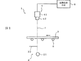
図1に、本発明による欠点検査装置1の第1の実施例の構成を示す。この欠点検出装置は、照明手段2と撮像手段4と画像処理手段6とを備えている。照明手段2は、照明手段の暗部を構成する遮光板22と、照明手段の明部を構成する光源21とから構成されている。撮像手段4は1次元走査を繰り返すラインセンサ(分解能50μm)であり、ラインセンサカメラ41とレンズ42とから構成されている。以上のような照明手段2と撮像手段4との間を、ガラス板3は搬送手段5によって搬送される。搬送方向は矢印で示すように、図において左方向である。ラインセンサ4からの1次元出力信号は、画像処理手段6へ送られ、画像処理手段では、1次元出力信号により画像データを形成し、この画像データを3値化処理し、3値化処理画像データに基づく画像を表示し、欠点を表す「明部」,「暗部」パターンを観察できるようにする。
照明手段2の明部を構成する光源21としては、直管の蛍光灯を用いた。通常の商用電源による点灯では、光量むらが大きいので、高周波点灯とした。なお、駆動周波数は30kHz以上とした。このように蛍光灯を高周波で点灯させる照明は安価であり、光量むらが少ないので好ましい。特に長さの長い光源が必要な場合に、蛍光灯を用いると有効である。
蛍光灯21の上方に、照明手段2の暗部を構成する遮光板22を配置した。配置する位置としては、ラインセンサ4の光軸7に遮光板のエッジが一致するようにして、光軸7に対してガラス板の搬送方向下流側である。遮光板22は、明部とのコントラストを大きくするために、黒色とするのが好ましく、艶消しとなっているとさらに好ましい。さらには、明部の明るさを大きくするには、図1に示すように、蛍光灯21の中心がラインセンサ4の光軸7に対して、右側へずれるように配置するのが望ましい。
図2は、ラインセンサ4の位置から照明手段側を見た図である。遮光板22が暗部を構成し、遮光板22で隠されていない蛍光灯21の発光表面が明部を構成している。明部と暗部の境にある×印の位置がラインセンサの視野中心である。そして、ラインセンサは、明部と暗部の境界部を1次元に走査して観察する。
照明手段の上方には、被検査対象物であるガラス板3を搬送するための搬送手段5が設けられている。図1においては、ローラによって矢印方向へ搬送を行っている。すなわち、照明手段2における明部と暗部の境界部の長さ方向が、搬送方向と直交している。
搬送手段の上方には、ラインセンサカメラ41およびレンズ42より構成されるラインセンサ4を設置している。このとき、ラインセンサカメラの観察範囲は、前述したように照明手段2の明部と暗部の境界部に合わせている。なお、ラインセンサカメラの観察可能な長さは決まっているので、被検査対象物の幅に合わせて、適宜設置台数を決めることができる。なお、ラインセンサカメラ42の焦点位置は、透明板近傍とする。好ましくは、透明板の表面とする。
画像処理手段6としては、例えばコンピュータを利用できる。ラインセンサの出力がアナログ信号の場合は、コンピュータにはデジタル信号に変換して取り込む必要があるので、画像出力手段6は、少なくともアナログ/デジタル変換機能を有する画像入力装置をさらに有することが要求される。ラインセンサカメラがデジタルカメラである場合には、アナログ/デジタル変換は不要である。
以上の欠点検出装置において、ガラス板3に欠点がある場合に、表示画像において欠点を表す「明部」,「暗部」よりなる欠点パターンを観察できる原理を、以下に説明する。
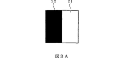
図1において、ラインセンサ4の位置から、ガラス板の表面上にある光学歪みを伴う凸部欠点を、目視して観察したときの照明手段の見え方を、模式的に図に示す。図3Aは、ガラス板に凸部欠点が無い場合を示す。左半分の黒地部分は照明手段の暗部である遮光板22を表し、右半分の白地部分は照明手段の明部である光源21の発光部分を表している。黒地部分と白地部分との境の上方にガラス板の凸部欠点があると、凸部欠点のレンズ作用によって光が屈折し、図3Bに10で示すように、明部21と暗部22との境の明部21背景中に暗部が、暗部22背景中に明部が表れる。図3A,図3Bは、あくまでも人間が目視により観察した場合であるが、焦点距離をガラス板表面に合わせたラインセンサで観察した場合には、明部21と暗部22との境がぼやけて見え、明部と暗部の明るさの比率により中間の明るさとなる。なお、この中間の明るさを、正確に明部の明るさと暗部の明るさとの中間の明るさに設定するためには、まず遮光板22を設けない状態でラインセンサの出力を求め、この出力を100とする。つぎに遮光板を設置して、ラインセンサの出力が50となるように、遮光板22の配置位置を調整することにより行う。
そして、ガラス板は搬送されているので、後述するように、ラインセンサはまず欠点10による光の屈折の結果、明部21を検出し、続いて暗部22を検出することになる。ラインセンサの出力信号を、画像処理手段で画像データにし、この画像データを3値化処理して画像表示すると、画像上には「明部」と「暗部」よりなるパターンが観察される。この「明暗」パターンが観察されれば、欠点は少なくとも凸部欠点であることが推定される。
以上は凸部欠点について、観察される欠点パターンについて説明したが、凸部欠点について、「明暗」パターンが発生する原理をさらに詳述すると共に、併せて泡欠点の場合に観察される欠点パターンについても説明する。
図4は、図3A,図3Bにおいて説明したと同様に、ガラス板の表面に凸部が存在する場合を説明するための図である。図4Aは、ラインセンサ4が、搬送されてくるガラス板3の表面の凸部31の前半部分を観察している状態を示す。ラインセンサ4に主として入射する光の光軸は、凸部31のレンズ作用により、遮光板22のエッジから蛍光灯21の発光面側へ偏移している。このため、光学歪みのない正常な部分を観察している場合に比べて、ラインセンサに入射する光量が増加する。
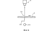
図4Bは、ラインセンサ4が、搬送されてくるガラス板の表面の凸部31の後半部分を観察している状態を示す。ラインセンサ4に主として入射する光の光軸は、凸部31のレンズ作用により、遮光板22のエッジから遮光板の内側へ偏移している。このため、光学歪みのない正常な部分を観察している場合に比べて、ラインセンサに入射する光量が減少する。
上述のような表面に凸部が存在するガラス板を移動させながらラインセンサで観察した場合、ラインセンサの出力1(明るさを表している)は図4Cのようになる。なお、図4Cは、ラインセンサの1画素における出力を示しており、横軸Lは、ガラス板の移動距離である。
図4Cにおいて、出力I0は、図3Aにおいて明部21と暗部22との境のぼやけた部分を観察している場合のラインセンサの前記画素の出力のレベルを示している。凸部欠点が移動してくると、ラインセンサの出力はまずレベルI0より大きくなり、続いてレベルI0より小さくなる。
ラインセンサの出力は、画像入力装置によりコンピュータに取り込まれ、画像データが形成される。この画像データは、3値化処理されて、3値化画像がディスプレイ上に表示される。ディスプレイ上には、凸部欠点の存在に対応して、「明部」と「暗部」がこの順で現れ、「明部」と「暗部」とよりなる「明暗」パターンが表示される。
なお光学歪みを伴う異物欠点の場合も、凸部欠点と同様に「明暗」パターンとして現れることが確かめられた。
また、ガラス板の表面に存在する凹部欠点の場合、3値化画像には、凸部欠点とは逆に、「暗明」パターンが現れることは、容易に理解できるであろう。さらに、ガラス板の表面に被覆された膜のピンホール欠点も、「暗明」パターンが現れることを確認している。
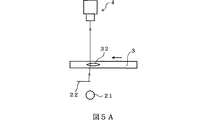
つぎに、ガラス板内に泡欠点が存在する場合の例を説明する。図5Aは、ラインセンサ4が、搬送されてくるガラス板内の泡欠点32の前半部を観察している状態を示す図である。ラインセンサ4に主として入射する光の光軸は、泡欠点のレンズ作用により、遮光板22のエッジから遮光板の内側へ偏移している。このため、正常な部分を観察している場合に比べて、ラインセンサに入射する光量が減少する。
図5Bは、ラインセンサ4が、搬送されてくるガラス板内の泡欠点32の後半部を観察している状態を示す。ラインセンサ4に主として入射する光の光軸は、泡欠点のレンズ作用により、遮光板22のエッジから蛍光灯21の発光面側へ偏移している。このため、正常な部分を観察している場合に比べて、ラインセンサに入射する光量が増加する。
上述のような泡欠点が存在するガラス板を移動させながらラインセンサで観察した場合、ラインセンサの1画素の出力Iは図5Cのようになる。泡部欠点が移動してくると、出力はまずレベルI0より小さくなり、続いてレベルI0より大きくなる。ラインセンサの出力は、コンピュータに取り込まれ、画像データが形成され、3値化処理される。泡欠点の存在に対応して、3値化画像上に「暗部」と「明部」がこの順で現れ、「暗部」と「明部」よりなる「暗明」パターンが表示される。
以上のように、欠点の種類によって、つまり光を屈折させる性質の違いによって、ガラス板の搬送方向に「明部」と「暗部」の現れる順序が決まり、「明部」と「暗部」とで構成される欠点パターンに違いが生じる。この欠点パターンの違いによって、欠点の種類を識別することができる。なおこのような欠点の種類の識別は、[発明の背景]で述べたように、日本国特許第3178644号公報に記載の遮光部と透光部が複数であるスリット板では困難であり、本発明の1次元の撮像手段に平行な直線状の透光部が1つしかない、言い換えれば複数でないスリット照明でのみ可能である。なお実際の欠点では、搬送方向以外も含めると「明部」と「暗部」よりなる複雑な欠点パターンを形成する場合が多いが、そのような欠点は、各種の欠点がまざり合った複合欠点と見なすことも可能である。
上述した検査装置によって、具体的にガラス板に存在する泡欠点を観察した例を示す。図6は、ラインセンサカメラ41からの信号を、画像入力装置にてコンピュータに取り込んで画像データを形成し、3値化処理を行うことなくディスプレイ上に表示した画像である。また、画面上の縦カーソルC1および横カーソルC2上における濃淡プロファイルも併せて示している。画像において、横方向はガラス板の搬送方向であり、縦方向はラインセンサの走査方向である。この画像では、画像の濃淡が不鮮明であり、したがって「明部」,「暗部」よりなる欠点パターンは不明瞭である。
本発明では、コンピュータにおいて、この2次元画像データについて、3値化処理を行い、明部と暗部とのコントラストを大きくする。3値化処理は、まず2次元画像データの全体の平均した明るさを求める。それを基準にして、+側と−側のしきい値を適宜設定して、+側のしきい値以上の画素データの部分を「明部」とし、−側のしきい値以下の画素データの部分を「暗部」とし、+側と−側のしきい値の間の範囲を「灰部」とする。なお、前記平均した明るさは、2次元画像データの全体から求めたが、これに限られるものではない。例えば、2次元画像の周辺部のみに対応する画像データから求めてもよい。
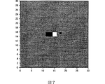
3値化された画像データをディスプレイに表示した画像を図7に示す。画像の濃淡がより鮮明になっている。このように3値化処理を行うと、「明部」,「暗部」よりなる欠点パターンを明瞭に表示することができる。
泡欠点の場合、ガラス板の搬送にしたがって、搬送方向にまず「暗部」が、続いて「明部」が現れ、「暗明」パターンを形成していることがわかる。図7に示した例では、「明部」パターンの後方ににさらに「暗部」が現れている。これは、泡欠点が大きく光学歪みが大きな場合に、観察している視野が蛍光灯の範囲から外れることによって起こる現象である。以上のことから、「暗明」パターンはラインセンサの分解能の整数倍を基準にして小さい泡欠点を示し、「暗明暗」パターンはラインセンサの分解能の整数倍を基準にして大きい泡欠点を示すことがわかる。
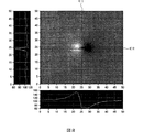
図8は、単純な凸部を伴う異物欠点を観察した場合の3値化処理前の画像データによる画像である。同様に3値化処理を行い、3値化された画像データによる画像を図9に示す。このような異物欠点の場合、ガラス板の進行にしたがって、まず「明部」が、続いて「暗部」が現れ、「明暗」パターンを形成していることがわかる。
以上、図1に示した欠点検査装置では、少なくとも異物欠点と泡欠点を区別することができる。
なお図1に示した欠点検査装置において、ガラス板3の搬送方向を逆にすれば、欠点パターンを構成する明部,暗部がガラス板の搬送方向に表れる順序は逆になることは、当業者には容易に理解できるであろう。
(実施例2)
上述した実施例1では、遮光板22を1枚用いた例であったが、この実施例ではさらに他の遮光板を追加して用いる。図10は、この例を示す図である。この他の遮光板23は、光源である蛍光灯21からの暗視野照明となる間接光を調整して、欠点からの乱反射光の発生を抑制するために設けている。このような遮光板23は、ラインセンサの視野に入らない範囲で、その位置を調整することができる。
図11は、図10の検査装置において、ラインセンサ4の位置から照明手段側を見た図である。遮光板22,23が暗部を構成し、遮光板22,23で隠されていない蛍光灯21の発光表面が明部21を構成している。明部21と暗部22の境にある×印の位置がラインセンサの視野中心である。
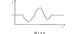
この検査装置を用いて、ラインセンサの分解能の整数倍を基準にして大きな泡欠点を検出すると、図6に示した様な「暗部」,「明部」,「暗部」が続く「暗明暗」パターンが発生しやすくなる。図12A,図12B,図12C,図12Dに、図5A,図5B,図5Cに対応した図を示し、「暗明暗」パターン発生の原理を示す。図12Aでは、泡欠点の先端部付近を観察しており、図12Dに示すようにラインセンサの出力がレベルI0より小さくなる。図12Bでは、泡欠点の中央部よりやや後方を観察しており、出力がレベルI0より大きくなり、図12Cでは、泡欠点の後端部付近を観察しており、出力がレベルI0より小さくなる。
つぎに、ガラス板上に存在する落下異物,落下異物の跡に存在するクレータ状の凹凸(この凹凸を落下異物跡という)の検査について説明する。
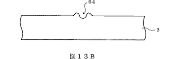
図13A,図13Bは、ガラス板3上に存在する、周りに盛り上がりを伴う落下異物と、クレータ状の凹凸である落下異物跡を示す。図13Aに示すように異物62が付着したままの落下異物欠点63は周りに盛り上がりを伴っており、3値化画像では凸部欠点と同様の「明暗」パターンを示した。この「明暗」パターンの例を、図14Aに示す。また、図13Bに示すようにクレータ状の落下異物跡欠点64は、3値化画像では「明暗明暗」パターンを示した。これらパターンを図14Bに示す。また、ラインセンサの分解能の整数倍を基準にして小さな落下異物跡は、「明暗」パターンになることを確かめた。
つぎに、図10に示した検査装置を用いて、ラインセンサの焦点位置をガラス板表面にし、ガラス板表面に付着した埃を観察した場合のパターンを図15に示す。図より明らかなように、埃では「暗部」しか観察されていないことがわかる。これは、付着している埃では、光を屈折することがないので、埃の存在によって遮光されることによって、入射光量が低下することのみを観察しているためである。
したがって、ラインセンサの焦点をガラス板表面にし、さらに遮光板23により乱反射光の発生を抑制することにより、3値化画像の「明部」,「暗部」のパターンを判断することで、光学歪みを伴う欠点と埃を区別することが可能である。
なお図10に示した欠点検査装置において、ガラス板3の搬送方向を逆にすれば、欠点パターンを構成する明部,暗部がガラス板の搬送方向に表れる順序は逆になることは、当業者には容易に理解できるであろう。
上記した埃と同様に、ガラス板表面に付着するものとして、ガラス板を切断したときの切断屑がある。このような切断屑は、光を屈折するので、光学歪みを伴う欠点と同様に検出することが可能である。ただし、切断屑の場合には、切断屑の大きさや形状に基づいて、「明部」および/または「暗部」よりなる複雑な欠点パターンを形成する場合が多い。
以上の実施例1,2では、照明手段2における明部と暗部の境界部の長さ方向と、透明板の搬送方向とは90°の角度をなしているが、90°に近い角度であってもよい。なお、ガラス製造における流れ方向の欠点を特に検出したい場合には、適宜斜めに交わらせるとよい。
(変形例)
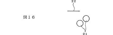
上述した実施例1では、照明手段を、1本の蛍光灯と、1枚の遮光板により構成したが、これに限るものではない。例えば、図16に示すように、2本の蛍光灯21を設けてもよい。
また、図17に示すように、複数本の蛍光灯21を配置し、上方に遮光板24と散乱板25とを設けた照明手段としてもよい。
また、図18に示すように、1本の蛍光灯21の表面に遮光膜26を直接形成して、照明手段としての明部と暗部を構成してもよい。
なお、以上の実施例および変形例では、光源として蛍光灯を用いたが、光源としては蛍光灯のほかに、例えばハロゲンランプを光源とし、ハロゲンランプからの光をファイバにて導いたファイバ照明でもよい。また棒状のLED照明を用いてもよい。
なお、本発明による検査方法が適用可能な透明板は、必ずしも平板に限られるものではなく、パネルなどのように、ゆるやかな曲率を有している板でもよい。また透明板は、適宜切断された板材でも、連続的に供給される板材でもよい。さらに本発明による検査方法は、透光性を有していれば半透明な板にも適用可能である。
産業上の利用可能性
以上詳細に説明してきたように本発明による検査方法および装置では、光学歪みを伴う欠点を、コントラストがはっきりした「明部」と「暗部」よりなるパターンとして観察することができ、さらには上記パターンの状態、すなわち「明部」と「暗部」とがシート状透明体の搬送方向に表れる順序,およびその組合せによって、欠点の種類を識別することが可能である。
また本発明による検査方法および装置では、透明板の表面に付着した除去可能で、欠点とならない埃も検出することが可能であるので、透明板の表面に存在する凹凸や透明板に内在する異物、泡等の欠点と区別して処理することができる。このため、特に清浄な空間において検査をする必要がなく、クリーンブース等の新たな設備を必要としないので、検査にかかるコストを抑えることができる。さらには、例えばハンドリングによる埃の付着が多いといった情報も得ることができる。この情報をもとに、工程の改善を図ることも可能である。
【図面の簡単な説明】
図1は、発明による検査装置の基本的構成を説明する概略図である。
図2は、図1においてラインセンサの位置から照明手段側を見た図である。
図3Aおよび図3Bは、照明手段を目視した場合に、その見え方を模式的に示す図である。
図4A,図4B,図4Cは、ガラス板の表面に凸部が存在する場合を説明する図である。
図5A,図5B,図5Cは、ガラス板内に泡欠点が存在する場合を説明する図である。
図6は、泡欠点を観察した画像データに基づく画像を示す図である。
図7は、泡欠点を観察した画像データを3値化処理し、3値化画像データに基づく画像を示す図である。
図8は、異物欠点を観察した画像データに基づく画像を示す図である。
図9は、異物欠点を観察した画像データを3値化処理し、3値化画像データに基づく画像を示す図である。
図10は、さらに他の遮蔽板を用いた検査装置を示す図である。
図11は、図10においてラインセンサの位置から照明手段側を見た図である。
図12A,図12B,図12C,図12Dは、図10の検査装置において、ガラス板内に泡欠点が存在する場合を説明する図である。
図13A,図13Bは、ガラス板上に存在する落下異物と、落下異物跡に存在するクレータ状の凹凸を示す図である。
図14A,図14Bは、落下異物欠点およびクレータ状欠点に対応する「明部」,「暗部」のパターンを示す図である。
図15は、埃を観察した画像データを3値化処理し、3値化画像データに基づく画像を示す図である。
図16は、他の照明手段を示す図である。
図17は、他の照明手段を示す図である。
図18は、さらに他の照明手段を示す図である。Technical field
The present invention relates to a defect inspection method and a defect inspection apparatus with optical distortion present in a sheet-like transparent body such as a transparent plate such as a glass plate or a transparent plate coated with a transparent film.
Background technology
Defects that exist on transparent plates, such as glass plates, include irregularities that exist on the surface, falling foreign objects that are defects caused by foreign matters that fall on the surface, crater-like irregularities that exist on the fallen foreign matter traces, foreign matters that exist inside, bubbles, etc. There is. Further, in the case of a glass plate whose surface is coated with a transparent film, a drawback of the transparent film is a pinhole. If these defects are accompanied by optical distortion, light is refracted by the optical distortion. For this reason, a glass plate or the like with optical distortion must be removed by inspection because it becomes a defective product and cannot be used as an optical substrate.
An optical distortion measuring method for inspecting and evaluating an optical distortion of a glass plate or the like is disclosed in Japanese Patent Application Laid-Open No. 8-247954. In the measurement method described in this publication, image information before the measurement object passes through the edge part of the boundary between the diffused light part and the light shielding part while changing the position of the measurement object relative to the light source and the image sensor. Optical distortion is measured using the absolute value of the difference from the later image information. However, the absolute value of the difference between the image information before passing through the edge portion and the image information after the edge portion cannot distinguish a defect having optical distortion, for example, a foreign object and a bubble.
Japanese Patent No. 3178644 (US Pat. No. 5,618,811A, EP 0726457A2) discloses a transparent plate through a slit plate in which a plurality of minute light-shielding portions and light-transmitting portions are provided alternately near the light source. A one-dimensional camera that projects light on the object and is placed on the opposite side of the light source across the transparent plate object, and when the image processing device detects defects, the camera focus is slit. When moving in the direction away from the plate, the gray state where the black (dark part) of the light shielding part of the slit plate and the white (bright part) of the translucent part overlap, that is, the maximum and minimum values of the combined waveform of the light and shade levels A transparent plate that can be distinguished from dust and dirt by determining that the vicinity of the position where the difference between them is zero first is the focus position for defect detection and that the obtained image signal is configured as a flag as a defect. Defect detection The law has been disclosed.
However, with this defect detection method, it is possible to distinguish and detect dust and dirt that do not have optical distortion, and defects that have optical distortion, but different defects with both optical distortion, such as foreign matter and bubbles. Cannot be distinguished. This is because a plurality of line-row slits in which the light projecting portion and the light-shielding portion are linearly arranged in parallel in one direction, or a plurality of grid-like slits in which line-row slits are placed in two directions and crossed, or in a checkered pattern. In a checker-like slit in which minute light-shielding portions and light-transmitting portions are alternately formed, there are a plurality of light-shielding portions and light-transmitting portions. Even if the pattern of the part and the dark part is the same type of defect, the pattern is not necessarily the same, and another type of defect may be the same pattern. For example, a foreign object in the transport direction of a transparent plate has a “bright, dark, dark” pattern, another foreign object has a “dark, dark” pattern, and a bubble has a “dark, dark” pattern. Can be considered.
Disclosure of invention
The objective of this invention is providing the method and apparatus which test | inspects the fault which has the optical distortion in a sheet-like transparent body so that the kind can be distinguished.
It is another object of the present invention to provide an apparatus for inspecting defects having optical distortion in a sheet-like transparent body so as to be distinguishable from dust attached to the surface of the sheet-like transparent body and having no optical distortion. is there.
The first aspect of the present invention is a defect inspection method for detecting a defect accompanied by optical distortion present in a sheet-like transparent material to be conveyed. In this defect inspection method, illumination means is provided on one side of the sheet-like transparent body, and one-dimensional imaging means is provided on the other side of the sheet-like transparent body. The illuminating means has a bright part and a dark part, and the boundary part between the bright part and the dark part is formed in a straight line substantially parallel to the one-dimensional imaging means, and the field of view of the imaging means is the boundary part. Two-dimensional image data is created from the one-dimensional output of the image pickup means, the image data is converted into ternary image data, and the display image based on the ternary image data is displayed in the transport direction of the sheet-like transparent body. A defect is detected and a defect type is identified by a defect pattern consisting of a bright part and a dark part that appear sequentially.
The second aspect of the present invention is a defect inspection apparatus for detecting a defect accompanied by optical distortion present in a sheet-like transparent body to be conveyed. This defect inspection apparatus includes a one-dimensional imaging unit provided on one side of a sheet-like transparent body, and an illumination unit provided on the other side of the sheet-like transparent body. The illuminating means has a bright part and a dark part, and a boundary part between the bright part and the dark part is formed in a straight line substantially parallel to the one-dimensional imaging means, and the field of view of the imaging means is the boundary part. Further, the image processing means includes image processing means for creating two-dimensional image data from the one-dimensional output of the imaging means, converting the image data into ternary image data, and forming a display image based on the ternary image data, In the display image, a defect pattern consisting of a bright portion and a dark portion that appear sequentially in the conveying direction of the sheet-like transparent body is displayed.
In the inspection method and apparatus of the present invention, the type of the defect is identified by the order in which the bright part and the dark part constituting the defect pattern appear in the transport direction of the sheet-like transparent body, and the combination of the bright part and the dark part. . The type of defect identified in this way is at least one of a foreign object defect, a bubble defect, a convex defect, a concave defect, a falling foreign object defect, and a falling foreign object defect.
BEST MODE FOR CARRYING OUT THE INVENTION
(Example 1)
FIG. 1 shows the configuration of a first embodiment of a
A straight fluorescent lamp was used as the
A
FIG. 2 is a view of the illumination unit side as seen from the position of the
Above the illuminating means, a conveying means 5 for conveying the
A
As the image processing means 6, for example, a computer can be used. When the output of the line sensor is an analog signal, it is necessary for the computer to convert the digital signal into a digital signal. Therefore, the image output means 6 is required to further include an image input device having at least an analog / digital conversion function. The When the line sensor camera is a digital camera, analog / digital conversion is not necessary.
In the above defect detection apparatus, when the
In FIG. 1, the appearance of the illumination means when the convex defect with optical distortion on the surface of the glass plate is visually observed from the position of the
And since the glass plate is conveyed, as will be described later, the line sensor first detects the
The above explains the observed defect pattern for the convex defect, but for the convex defect, the principle of generating the “bright” pattern is explained in detail, and the defect pattern observed in the case of the bubble defect is also described. Also explained.
FIG. 4 is a diagram for explaining a case where a convex portion exists on the surface of the glass plate, as described in FIGS. 3A and 3B. FIG. 4A shows a state where the
FIG. 4B shows a state where the
When observed with a line sensor while moving a glass plate having convex portions on the surface as described above, the output 1 (representing brightness) of the line sensor is as shown in FIG. 4C. FIG. 4C shows the output in one pixel of the line sensor, and the horizontal axis L is the moving distance of the glass plate.
In FIG. 4C, output I 0 FIG. 3A shows the output level of the pixel of the line sensor when the blurred part of the boundary between the
The output of the line sensor is taken into a computer by an image input device, and image data is formed. This image data is ternarized and a ternary image is displayed on the display. On the display, “bright part” and “dark part” appear in this order corresponding to the presence of the convex defect, and a “bright” pattern consisting of “bright part” and “dark part” is displayed.
In addition, it was confirmed that the foreign substance defect accompanied by optical distortion appears as a “bright” pattern as well as the convex defect.
In the case of a concave defect present on the surface of the glass plate, it can be easily understood that a “dark” pattern appears in the ternary image, contrary to the convex defect. Furthermore, the pinhole defect of the film | membrane coat | covered on the surface of the glass plate has confirmed that the "dark" pattern appears.
Next, an example where a bubble defect exists in the glass plate will be described. FIG. 5A is a diagram illustrating a state in which the
FIG. 5B shows a state in which the
When the line sensor is observed while moving the glass plate having the bubble defect as described above, the output I of one pixel of the line sensor is as shown in FIG. 5C. When the bubble defect moves, the output is first level I 0 Smaller, then level I 0 Become bigger. The output of the line sensor is captured by a computer, image data is formed, and ternary processing is performed. Corresponding to the presence of bubble defects, “dark part” and “bright part” appear in this order on the ternary image, and a “dark part” pattern consisting of “dark part” and “bright part” is displayed.
As described above, the order in which the “bright part” and “dark part” appear in the transport direction of the glass plate is determined by the type of defect, that is, the difference in the property of refracting light. There is a difference in the configured defect pattern. The type of defect can be identified by the difference in defect pattern. In addition, as described in [Background of the Invention], it is difficult to identify such types of defects with a slit plate having a plurality of light-shielding portions and light-transmitting portions described in Japanese Patent No. 3178644. Only one linear light-transmitting portion parallel to the one-dimensional imaging means of the invention is available, in other words, it is possible only with a plurality of slit illuminations. In addition, in actual defects, including other than the conveyance direction, complex defect patterns consisting of “bright parts” and “dark parts” are often formed. However, such defects are complex defects in which various defects are mixed together. It can also be considered.
The example which observed the bubble defect which specifically exists in a glass plate with the inspection apparatus mentioned above is shown. FIG. 6 shows an image displayed on a display without performing a ternarization process by inputting a signal from the
In the present invention, the computer performs ternarization processing on the two-dimensional image data to increase the contrast between the bright part and the dark part. In the ternary processing, first, the average brightness of the entire two-dimensional image data is obtained. Based on this, the threshold values on the + side and − side are appropriately set, the pixel data portion above the + side threshold value is defined as “bright”, and the pixel data below the − side threshold value Is the “dark part”, and the range between the positive and negative thresholds is the “ash part”. In addition, although the said average brightness was calculated | required from the whole two-dimensional image data, it is not restricted to this. For example, you may obtain | require from the image data corresponding only to the peripheral part of a two-dimensional image.
An image obtained by displaying the ternary image data on the display is shown in FIG. The shading of the image is clearer. By performing the ternarization process in this way, it is possible to clearly display a defect pattern composed of “bright parts” and “dark parts”.
In the case of a bubble defect, it can be seen that a “dark portion” first appears in the transport direction and then a “bright portion” appears in the transport direction as the glass plate is transported, forming a “dark light” pattern. In the example shown in FIG. 7, a “dark part” appears further behind the “bright part” pattern. This is a phenomenon that occurs when the field of view deviates from the fluorescent lamp range when the bubble defect is large and the optical distortion is large. From the above, the “dark / light” pattern shows a small bubble defect based on an integer multiple of the line sensor resolution, and the “dark / dark” pattern shows a large bubble defect based on an integer multiple of the line sensor resolution. I understand that.
FIG. 8 is an image based on image data before ternarization processing when a foreign object defect with a simple convex portion is observed. Similarly, ternarization processing is performed, and an image based on the ternarized image data is shown in FIG. In the case of such a foreign substance defect, it can be seen that a “bright part” appears first, followed by a “dark part” as the glass plate advances, forming a “bright” pattern.
As described above, the defect inspection apparatus shown in FIG. 1 can distinguish at least a foreign substance defect and a bubble defect.
In the defect inspection apparatus shown in FIG. 1, if the conveyance direction of the
(Example 2)
In the first embodiment described above, one
FIG. 11 is a view of the illumination device side as seen from the position of the
When a large bubble defect is detected using this inspection apparatus with an integer multiple of the resolution of the line sensor as a reference, the “dark part”, “bright part”, and “dark part” as shown in FIG. Patterns are likely to occur. FIGS. 12A, 12B, 12C, and 12D show diagrams corresponding to FIGS. 5A, 5B, and 5C, and show the principle of “dark / dark” pattern generation. In FIG. 12A, the vicinity of the tip of the bubble defect is observed, and the output of the line sensor is level I as shown in FIG. 12D. 0 Smaller. In FIG. 12B, the back of the bubble defect is observed slightly from the center, and the output is level I. 0 In FIG. 12C, the vicinity of the rear end of the bubble defect is observed, and the output is level I. 0 Smaller.
Next, the inspection of the fallen foreign matter existing on the glass plate and the crater-like irregularities present on the trace of the fallen foreign matter (this irregularity is referred to as the fallen foreign matter trace) will be described.
FIG. 13A and FIG. 13B show the fallen foreign matter with swell around it and the fallen foreign matter traces that are crater-like irregularities present on the
Next, FIG. 15 shows a pattern when the focus position of the line sensor is set to the surface of the glass plate and dust attached to the surface of the glass plate is observed using the inspection apparatus shown in FIG. As can be seen from the figure, only "dark parts" are observed in dust. This is because the adhering dust does not refract light, and thus only observes that the amount of incident light is reduced by being blocked by the presence of dust.
Accordingly, the focal point of the line sensor is the surface of the glass plate, and the generation of irregularly reflected light is suppressed by the
In the defect inspection apparatus shown in FIG. 10, if the conveyance direction of the
Similar to the dust described above, there is a cutting waste when the glass plate is cut as a material that adheres to the surface of the glass plate. Since such cutting waste refracts light, it can be detected in the same manner as a defect with optical distortion. However, in the case of cutting waste, a complicated defect pattern composed of “bright portions” and / or “dark portions” is often formed based on the size and shape of the cutting waste.
In Examples 1 and 2 above, the length direction of the boundary between the bright part and the dark part in the
(Modification)
In the first embodiment described above, the illumination unit is configured by one fluorescent lamp and one light shielding plate, but is not limited thereto. For example, as shown in FIG. 16, two
Moreover, as shown in FIG. 17, it is good also as an illuminating means which has arrange | positioned the several
Further, as shown in FIG. 18, a
In the above embodiments and modifications, a fluorescent lamp is used as a light source. However, in addition to a fluorescent lamp, a light source such as a halogen lamp is used as a light source, and fiber illumination in which light from the halogen lamp is guided by a fiber is also used. Good. Moreover, you may use rod-shaped LED illumination.
The transparent plate to which the inspection method according to the present invention can be applied is not necessarily limited to a flat plate, and may be a plate having a gentle curvature such as a panel. Further, the transparent plate may be a plate material that is appropriately cut or a plate material that is continuously supplied. Furthermore, the inspection method according to the present invention can be applied to a translucent plate as long as it has translucency.
Industrial applicability
As described above in detail, in the inspection method and apparatus according to the present invention, the defect accompanied by optical distortion can be observed as a pattern composed of a “bright part” and a “dark part” with a clear contrast. It is possible to identify the type of defect by the state, that is, the order in which the “bright part” and the “dark part” appear in the transport direction of the sheet-like transparent body, and the combination thereof.
Further, in the inspection method and apparatus according to the present invention, it is possible to detect dust that is attached to the surface of the transparent plate and can be removed, and dust that does not become a defect can be detected. It can be treated separately from defects such as bubbles. For this reason, it is not necessary to perform inspection in a particularly clean space, and no new equipment such as a clean booth is required, so that the cost for inspection can be reduced. Furthermore, for example, it is possible to obtain information that dust is frequently attached by handling. It is also possible to improve the process based on this information.
[Brief description of the drawings]
FIG. 1 is a schematic diagram illustrating a basic configuration of an inspection apparatus according to the invention.
FIG. 2 is a diagram of the illumination means side as viewed from the position of the line sensor in FIG.
FIG. 3A and FIG. 3B are diagrams schematically showing how the illuminating means looks when viewed.
FIG. 4A, FIG. 4B, and FIG. 4C are diagrams illustrating a case where a convex portion exists on the surface of the glass plate.
FIG. 5A, FIG. 5B, and FIG. 5C are figures explaining the case where a bubble defect exists in a glass plate.
FIG. 6 is a diagram illustrating an image based on image data obtained by observing a bubble defect.
FIG. 7 is a diagram illustrating an image based on the ternary image data obtained by ternarizing the image data in which the bubble defect is observed.
FIG. 8 is a diagram illustrating an image based on image data obtained by observing a foreign substance defect.
FIG. 9 is a diagram illustrating an image based on the ternarized image data after the ternarization processing is performed on the image data in which the foreign object defect is observed.
FIG. 10 is a diagram showing an inspection apparatus using still another shielding plate.
FIG. 11 is a view of the illumination unit side as seen from the position of the line sensor in FIG.
12A, FIG. 12B, FIG. 12C, and FIG. 12D are diagrams for explaining a case where a bubble defect exists in the glass plate in the inspection apparatus of FIG.
FIG. 13A and FIG. 13B are diagrams showing falling foreign matter present on the glass plate and crater-like irregularities present on the falling foreign matter trace.
14A and 14B are diagrams showing patterns of “bright parts” and “dark parts” corresponding to the fallen foreign object defects and the crater-like defects.
FIG. 15 is a diagram illustrating an image based on the ternary image data obtained by ternarizing image data obtained by observing dust.
FIG. 16 is a diagram showing another illumination means.
FIG. 17 is a diagram showing another illumination means.
FIG. 18 is a diagram showing still another illumination means.
Claims (8)
前記シート状透明体の一方の側に設けられた1次元の撮像手段と、
前記シート状透明体の他方の側に設けられた照明手段とを備え、
前記照明手段は明部と暗部を有し、前記照明手段の明部と暗部は、直線状の光源と、前記光源と前記シート状透明体の間に設けられ、前記光源の長手方向に平行に延びるエッジ部を有し、前記エッジ部を含む側が前記光源の一部分を長手方向に沿って覆うように配置された第1の遮光板とで形成され、前記明部と暗部との境界部は、前記直線状の光源に平行な直線状をなし、前記第1の遮光板のエッジ部は、前記撮像手段の光軸に位置するように配置され、前記撮像手段の観察範囲を前記境界部とし、
前記光源と前記シート状透明体との間に設けられ、前記第1の遮光板のエッジ部に平行に延びるエッジ部を有し、前記光源からの暗視野照明となる間接光を調整して欠点が乱反射光を発生することを抑制するための第2の遮光板を、前記照明手段がさらに備え、
前記シート状透明体が、前記直線状の境界部と直交する方向に搬送されるときに、前記撮像手段は前記境界部を観察し、前記撮像手段の1次元出力から2次元の画像データを作成し、画像データを3値化処理した画像データに変換し、3値化画像データに基づく表示画像を形成する画像処理手段を備え、前記表示画像中に、前記シート状透明体の搬送方向に順次表れる明部,暗部よりなる欠点パターンを表示することを特徴とする欠点検査装置。In the defect inspection apparatus for detecting defects with optical distortion present in the sheet-like transparent material being conveyed,
One-dimensional imaging means provided on one side of the sheet-like transparent body;
Illuminating means provided on the other side of the sheet-like transparent body,
The illumination means has a bright part and a dark part, and the bright part and the dark part of the illumination means are provided between a linear light source, the light source and the sheet-like transparent body, and are parallel to the longitudinal direction of the light source. An edge part extending, and a side including the edge part is formed with a first light-shielding plate arranged so as to cover a part of the light source along a longitudinal direction, and a boundary part between the bright part and the dark part, A linear shape parallel to the linear light source is formed, the edge portion of the first light shielding plate is disposed so as to be positioned on the optical axis of the imaging means, and the observation range of the imaging means is the boundary portion,
Disadvantage of adjusting indirect light that is provided between the light source and the sheet-like transparent body and has an edge portion extending in parallel with the edge portion of the first light-shielding plate and serving as dark field illumination from the light source The illumination means further comprises a second light shielding plate for suppressing the generation of irregularly reflected light,
When the sheet-like transparent body is conveyed in a direction perpendicular to the linear boundary portion, the imaging means observes the boundary portion and creates two-dimensional image data from the one-dimensional output of the imaging means. And image processing means for converting the image data into ternarized image data and forming a display image based on the ternary image data, and sequentially in the transport direction of the sheet-like transparent body in the display image A defect inspection apparatus characterized by displaying a defect pattern consisting of a bright part and a dark part appearing.
前記欠点の種類の識別は、前記欠点パターンを構成する明部,暗部が前記シート状透明体の搬送方向に表れる順序、および明部,暗部の組合わせにより行うことを特徴とする欠点検査装置。The defect inspection apparatus according to claim 1,
The defect type identification apparatus is characterized in that the type of defect is identified by the order in which the bright and dark parts constituting the defect pattern appear in the transport direction of the sheet-like transparent body, and the combination of the bright and dark parts.
前記1次元の撮像手段は、レンズとラインセンサカメラとにより構成されることを特徴とする欠点検査装置。The defect inspection apparatus according to claim 1 or 2,
The defect inspection apparatus according to claim 1, wherein the one-dimensional image pickup means includes a lens and a line sensor camera.
前記直線状の光源は直管の蛍光灯であることを特徴とする欠点検査装置。The defect inspection apparatus according to claim 1, 2 or 3,
The defect inspection apparatus, wherein the linear light source is a straight tube fluorescent lamp.
前記蛍光灯は、30kHz以上で高周波点灯させることを特徴とする欠点検査装置。The defect inspection apparatus according to claim 4,
The defect inspection apparatus, wherein the fluorescent lamp is lit at a high frequency of 30 kHz or more.
前記第1および2の遮光板は、黒色であることを特徴とする欠点検査装置。In the defect inspection apparatus according to any one of claims 1 to 5,
The defect inspection apparatus, wherein the first and second light shielding plates are black.
前記シート状透明体は、ガラス板であることを特徴とする欠点検査装置。In the defect inspection device according to any one of claims 1 to 6,
The defect inspection apparatus, wherein the sheet-like transparent body is a glass plate.
前記シート状透明体は、透明膜が被覆されたガラス板であることを特徴とする欠点検査装置。In the defect inspection device according to any one of claims 1 to 6,
The defect inspection apparatus, wherein the sheet-like transparent body is a glass plate coated with a transparent film.
Applications Claiming Priority (3)
| Application Number | Priority Date | Filing Date | Title |
|---|---|---|---|
| JP2001204571 | 2001-07-05 | ||
| JP2001204571 | 2001-07-05 | ||
| PCT/JP2002/006720 WO2003005007A1 (en) | 2001-07-05 | 2002-07-03 | Method and device for inspecting defect of sheet-shaped transparent body |
Publications (2)
| Publication Number | Publication Date |
|---|---|
| JPWO2003005007A1 JPWO2003005007A1 (en) | 2004-10-28 |
| JP4132046B2 true JP4132046B2 (en) | 2008-08-13 |
Family
ID=19041012
Family Applications (1)
| Application Number | Title | Priority Date | Filing Date |
|---|---|---|---|
| JP2003510932A Expired - Fee Related JP4132046B2 (en) | 2001-07-05 | 2002-07-03 | Device for inspecting defects of sheet-like transparent body |
Country Status (5)
| Country | Link |
|---|---|
| US (1) | US6930772B2 (en) |
| JP (1) | JP4132046B2 (en) |
| KR (1) | KR20040015728A (en) |
| CN (1) | CN1293381C (en) |
| WO (1) | WO2003005007A1 (en) |
Cited By (1)
| Publication number | Priority date | Publication date | Assignee | Title |
|---|---|---|---|---|
| JP2010091460A (en) * | 2008-10-09 | 2010-04-22 | Nippon Steel Corp | Device and method for detecting hole defect |
Families Citing this family (52)
| Publication number | Priority date | Publication date | Assignee | Title |
|---|---|---|---|---|
| DE10316707B4 (en) * | 2003-04-04 | 2006-04-27 | Schott Ag | Method and device for detecting defects in transparent material |
| US7160479B2 (en) * | 2004-01-20 | 2007-01-09 | Ppg Industries Ohio, Inc. | Method and apparatus for evaluating panel drip tests |
| WO2006039192A1 (en) * | 2004-09-29 | 2006-04-13 | Telco Testing Solutions, Llc | Apparatus and method for detection of contaminant particles or component defects |
| KR100642500B1 (en) * | 2005-03-02 | 2006-11-06 | (주)쎄미시스코 | Edge defect and discolor inspection device of glass substrate |
| KR101166828B1 (en) * | 2005-12-29 | 2012-07-19 | 엘지디스플레이 주식회사 | Apparatus for Testing flat panel display device and testing method thereof |
| JP2007192660A (en) * | 2006-01-19 | 2007-08-02 | Fujifilm Corp | Film surface defect detection method and detector |
| DE102006051538B4 (en) * | 2006-10-27 | 2009-04-09 | Schott Ag | Method and device for determining the waviness of glass panes |
| JP2009047517A (en) * | 2007-08-17 | 2009-03-05 | Kokusai Gijutsu Kaihatsu Co Ltd | Inspection device |
| CN101576492A (en) * | 2008-05-09 | 2009-11-11 | 鸿富锦精密工业(深圳)有限公司 | Film plating substrate detection device and film plating substrate detection method |
| DE102008027653B4 (en) * | 2008-06-10 | 2012-11-08 | Basler Ag | Method for increasing the contrast |
| JP2010048745A (en) * | 2008-08-25 | 2010-03-04 | Asahi Glass Co Ltd | Defect inspection system and defect inspection method |
| CN102334025A (en) * | 2009-04-09 | 2012-01-25 | 旭硝子株式会社 | Method for detecting ream of light-transmitting platy object |
| EP2253948B1 (en) * | 2009-05-22 | 2013-01-09 | Dr. Schenk GmbH Industriemesstechnik | Device and method for optical examination of an object |
| CN101936916A (en) * | 2009-07-02 | 2011-01-05 | 法国圣-戈班玻璃公司 | Apparatus and method for detecting defects in separated low stiffness transparent or translucent bodies |
| JP5563388B2 (en) * | 2010-06-30 | 2014-07-30 | 第一実業ビスウィル株式会社 | Chip LED inspection device |
| DE102010046433B4 (en) * | 2010-09-24 | 2012-06-21 | Grenzebach Maschinenbau Gmbh | Apparatus and method for detecting defects in continuously generated float glass |
| DE102010037788B4 (en) * | 2010-09-27 | 2012-07-19 | Viprotron Gmbh | Method and device for displaying automatically determined fault locations |
| KR20140001927A (en) * | 2010-12-01 | 2014-01-07 | 아사히 가라스 가부시키가이샤 | Molten glass examination device |
| CN103250047A (en) * | 2010-12-09 | 2013-08-14 | 旭硝子株式会社 | Method for measuring defects in glass ribbon and system for measuring defects in glass ribbon |
| KR20140022064A (en) * | 2011-05-10 | 2014-02-21 | 아사히 가라스 가부시키가이샤 | Method for inspecting minute defect of translucent board-like body, and apparatus for inspecting minute defect of translucent board-like body |
| EP2631593A1 (en) * | 2012-02-24 | 2013-08-28 | Fraunhofer Gesellschaft zur Förderung der angewandten Wissenschaft E.V. | Method for detecting surface defects of a level surface |
| JP5808015B2 (en) * | 2012-03-23 | 2015-11-10 | 富士フイルム株式会社 | Defect inspection method |
| KR101330098B1 (en) * | 2012-05-10 | 2013-11-18 | 동우 화인켐 주식회사 | Method for discriminating defect of optical films |
| TWI607212B (en) * | 2013-01-16 | 2017-12-01 | 住友化學股份有限公司 | Image generation device, defect inspection device, and defect inspection method |
| JP6179886B2 (en) * | 2013-04-09 | 2017-08-16 | 住友化学株式会社 | Defect inspection apparatus, optical display device production system, and optical sheet manufacturing system |
| CN103623708B (en) * | 2013-12-12 | 2015-05-20 | 天津理工大学 | Detection device and detection method for atmospheric particulate collecting filter membrane pinholes |
| CN103868478A (en) * | 2014-04-01 | 2014-06-18 | 四川虹视显示技术有限公司 | Rapid detection method and device for flatness of transparent flat plate |
| CN103983430A (en) * | 2014-04-25 | 2014-08-13 | 中国科学院长春光学精密机械与物理研究所 | Device and method for testing out-band relative spectral responsivity of solar blind ultraviolet image intensifier |
| JP6459026B2 (en) * | 2014-07-08 | 2019-01-30 | 株式会社メック | Defect inspection apparatus and defect inspection method |
| JP6436664B2 (en) | 2014-07-14 | 2018-12-12 | 住友化学株式会社 | Substrate inspection apparatus and substrate inspection method |
| CN104865272A (en) * | 2015-05-11 | 2015-08-26 | 天津三瑞塑胶制品有限公司 | Glass adhesive tape appearance tester |
| TW201818065A (en) * | 2016-09-01 | 2018-05-16 | 美商3M新設資產公司 | Machine direction line film inspection |
| KR101719964B1 (en) | 2016-11-10 | 2017-03-24 | (주)글로텍 | Screw-rotor |
| EP3553501B1 (en) * | 2016-12-09 | 2022-07-20 | Otsuka Pharmaceutical Co., Ltd. | Measurement abnormality detecting method |
| JP6788837B2 (en) * | 2017-01-06 | 2020-11-25 | 日本電気硝子株式会社 | Glass plate inspection method and its manufacturing method and glass plate inspection equipment |
| JP6874441B2 (en) * | 2017-03-16 | 2021-05-19 | コニカミノルタ株式会社 | Defect inspection methods, defect inspection programs, and defect inspection equipment |
| JP6970549B2 (en) * | 2017-07-24 | 2021-11-24 | 住友化学株式会社 | Defect inspection system and defect inspection method |
| JP2019023587A (en) * | 2017-07-24 | 2019-02-14 | 住友化学株式会社 | Defect inspection system and defect inspection method |
| CN109387525A (en) * | 2017-08-09 | 2019-02-26 | 苏州精濑光电有限公司 | On a kind of film in film defect determination method |
| CN107392906B (en) * | 2017-08-10 | 2020-09-25 | 芜湖德海机器人科技有限公司 | Glass cleaning method based on multiple image acquisition and mechanical arm |
| CN107481230B (en) * | 2017-08-10 | 2020-09-25 | 芜湖德海机器人科技有限公司 | An intelligent glass cleaning robot hand control system based on image acquisition |
| CN109781743A (en) * | 2017-11-14 | 2019-05-21 | 鹤立精工股份有限公司 | Optical detection method |
| TWI705244B (en) * | 2018-07-31 | 2020-09-21 | 由田新技股份有限公司 | Semiconductor defects inspection apparatus |
| US11385039B2 (en) * | 2018-09-19 | 2022-07-12 | Corning Incorporated | Methods of measuring a size of edge defects of glass sheets using an edge defect gauge and corresponding edge defect gauge |
| JP2020091132A (en) * | 2018-12-04 | 2020-06-11 | 株式会社小糸製作所 | Surface defect inspection device of translucent member |
| EP3838470A1 (en) * | 2019-12-17 | 2021-06-23 | Bystronic Laser AG | Detection of foreign bodies and slag detection on a work desk |
| CN113686879A (en) * | 2021-09-09 | 2021-11-23 | 杭州利珀科技有限公司 | Optical film defect visual detection system and method |
| CN114660090B (en) * | 2022-02-24 | 2025-09-30 | 彩虹显示器件股份有限公司 | Device and method for detecting inclusion defects and deformation of flat glass using a knife block |
| CN115236946B (en) * | 2022-07-25 | 2026-01-30 | 上海积塔半导体有限公司 | Lens defect detection method, device, and semiconductor structure fabrication method |
| CN116216378B (en) * | 2022-11-24 | 2025-11-18 | 苏州德聚春田材料科技有限公司 | Dual inspection equipment for cross-line defects in polycarbonate film extrusion |
| CN115876784B (en) * | 2023-01-31 | 2023-05-26 | 眉山博雅新材料股份有限公司 | A workpiece defect detection method, system and device |
| CN117491391B (en) * | 2023-12-29 | 2024-03-15 | 登景(天津)科技有限公司 | Glass substrate light three-dimensional health detection method and equipment based on chip calculation |
Family Cites Families (12)
| Publication number | Priority date | Publication date | Assignee | Title |
|---|---|---|---|---|
| FI80959C (en) * | 1988-04-21 | 1990-08-10 | Outokumpu Oy | FOERFARANDE OCH ANORDNING FOER INSPEKTION AV SPEGELREFLEXIONSYTOR. |
| DE4031633A1 (en) * | 1990-10-05 | 1992-04-16 | Sick Optik Elektronik Erwin | OPTICAL INSPECTION DEVICE |
| JP2795595B2 (en) * | 1992-06-26 | 1998-09-10 | セントラル硝子株式会社 | Defect detection method for transparent plate |
| JPH08128968A (en) * | 1994-10-31 | 1996-05-21 | Sumitomo Chem Co Ltd | Defect inspection method for transparent sheet moldings |
| JPH08178855A (en) | 1994-12-20 | 1996-07-12 | Asahi Glass Co Ltd | Inspection method for translucent or specular objects |
| JP3178644B2 (en) * | 1995-02-10 | 2001-06-25 | セントラル硝子株式会社 | Defect detection method for transparent plate |
| JPH08247954A (en) * | 1995-03-15 | 1996-09-27 | Asahi Glass Co Ltd | Optical distortion measurement method |
| US5870203A (en) * | 1996-03-15 | 1999-02-09 | Sony Corporation | Adaptive lighting control apparatus for illuminating a variable-speed web for inspection |
| DE19643018B4 (en) * | 1996-10-18 | 2010-06-17 | Isra Surface Vision Gmbh | Method and device for measuring the course of reflective surfaces |
| DE19813072A1 (en) * | 1998-03-25 | 1999-09-30 | Laser Sorter Gmbh | Method and device for determining the optical quality and for detecting defects in flat glass and other optically transparent materials |
| DE19813073A1 (en) * | 1998-03-25 | 1999-09-30 | Laser Sorter Gmbh | Method and device for determining the optical quality and for detecting defects in flat glass and other optically transparent materials, in particular drips, threads and lines |
| JP2004125661A (en) * | 2002-10-03 | 2004-04-22 | Fuji Photo Film Co Ltd | Surface distortion inspection device for magnetic tape |
-
2002
- 2002-07-03 US US10/473,442 patent/US6930772B2/en not_active Expired - Fee Related
- 2002-07-03 CN CNB028094824A patent/CN1293381C/en not_active Expired - Fee Related
- 2002-07-03 KR KR10-2003-7015820A patent/KR20040015728A/en not_active Ceased
- 2002-07-03 JP JP2003510932A patent/JP4132046B2/en not_active Expired - Fee Related
- 2002-07-03 WO PCT/JP2002/006720 patent/WO2003005007A1/en not_active Ceased
Cited By (1)
| Publication number | Priority date | Publication date | Assignee | Title |
|---|---|---|---|---|
| JP2010091460A (en) * | 2008-10-09 | 2010-04-22 | Nippon Steel Corp | Device and method for detecting hole defect |
Also Published As
| Publication number | Publication date |
|---|---|
| WO2003005007A1 (en) | 2003-01-16 |
| JPWO2003005007A1 (en) | 2004-10-28 |
| CN1520512A (en) | 2004-08-11 |
| CN1293381C (en) | 2007-01-03 |
| US6930772B2 (en) | 2005-08-16 |
| US20040179193A1 (en) | 2004-09-16 |
| KR20040015728A (en) | 2004-02-19 |
Similar Documents
| Publication | Publication Date | Title |
|---|---|---|
| JP4132046B2 (en) | Device for inspecting defects of sheet-like transparent body | |
| KR101442871B1 (en) | Sheet material lighting system and method | |
| KR101326455B1 (en) | Apparatus and method for characterizing defects in a transparent substrate | |
| JP2795595B2 (en) | Defect detection method for transparent plate | |
| CN1965222B (en) | Devices for controlling transparent or reflective elements | |
| US20040000652A1 (en) | Dual level out-of-focus light source for amplification of defects on a surface | |
| CN110736751B (en) | Surface defect detection method and device | |
| JPH08278257A (en) | Moving-object inspecting method | |
| CN113686879A (en) | Optical film defect visual detection system and method | |
| JP4511978B2 (en) | Surface flaw inspection device | |
| CN103858000A (en) | Method and device for the reliable detection of material defects in transparent material | |
| JP2011085520A (en) | Defect discrimination device, defect discrimination method, and sheet-like material | |
| JP2013246059A (en) | Defect inspection apparatus and defect inspection method | |
| JP2011145082A (en) | Surface defect inspection device for sheet-like object | |
| JPH10176995A (en) | Transparent object inspection method and apparatus | |
| JP6679942B2 (en) | Sheet defect inspection device | |
| JP2012247343A (en) | Defect inspection method of antireflection film and defect inspection apparatus | |
| JP2005083906A (en) | Defect detector | |
| JP2014169988A (en) | Defect inspection device of transparent body or reflection body | |
| JPH06242019A (en) | Method and device for inspecting paint surface by image signal | |
| JPH09113465A (en) | Surface defect detector for galvanized steel sheet | |
| JP2011043415A (en) | Detection method and device of deposit on glass plate surface | |
| JP2007333608A (en) | Inspection device and inspection method for uneven defects in sheet | |
| JP7545176B1 (en) | Defect inspection device and defect inspection method | |
| CN219737320U (en) | Coating film apron detection device |
Legal Events
| Date | Code | Title | Description |
|---|---|---|---|
| A621 | Written request for application examination |
Free format text: JAPANESE INTERMEDIATE CODE: A621 Effective date: 20050310 |
|
| A521 | Request for written amendment filed |
Free format text: JAPANESE INTERMEDIATE CODE: A523 Effective date: 20050330 |
|
| A131 | Notification of reasons for refusal |
Free format text: JAPANESE INTERMEDIATE CODE: A131 Effective date: 20071127 |
|
| A521 | Request for written amendment filed |
Free format text: JAPANESE INTERMEDIATE CODE: A523 Effective date: 20080124 |
|
| TRDD | Decision of grant or rejection written | ||
| A01 | Written decision to grant a patent or to grant a registration (utility model) |
Free format text: JAPANESE INTERMEDIATE CODE: A01 Effective date: 20080401 |
|
| A01 | Written decision to grant a patent or to grant a registration (utility model) |
Free format text: JAPANESE INTERMEDIATE CODE: A01 |
|
| A61 | First payment of annual fees (during grant procedure) |
Free format text: JAPANESE INTERMEDIATE CODE: A61 Effective date: 20080530 |
|
| FPAY | Renewal fee payment (event date is renewal date of database) |
Free format text: PAYMENT UNTIL: 20110606 Year of fee payment: 3 |
|
| R150 | Certificate of patent or registration of utility model |
Free format text: JAPANESE INTERMEDIATE CODE: R150 |
|
| FPAY | Renewal fee payment (event date is renewal date of database) |
Free format text: PAYMENT UNTIL: 20110606 Year of fee payment: 3 |
|
| FPAY | Renewal fee payment (event date is renewal date of database) |
Free format text: PAYMENT UNTIL: 20120606 Year of fee payment: 4 |
|
| LAPS | Cancellation because of no payment of annual fees |