JP4135594B2 - 固体撮像装置 - Google Patents
固体撮像装置 Download PDFInfo
- Publication number
- JP4135594B2 JP4135594B2 JP2003294938A JP2003294938A JP4135594B2 JP 4135594 B2 JP4135594 B2 JP 4135594B2 JP 2003294938 A JP2003294938 A JP 2003294938A JP 2003294938 A JP2003294938 A JP 2003294938A JP 4135594 B2 JP4135594 B2 JP 4135594B2
- Authority
- JP
- Japan
- Prior art keywords
- capacitor
- pixel
- signal line
- transistor
- switch means
- Prior art date
- Legal status (The legal status is an assumption and is not a legal conclusion. Google has not performed a legal analysis and makes no representation as to the accuracy of the status listed.)
- Expired - Fee Related
Links
Images


Classifications
-
- H—ELECTRICITY
- H10—SEMICONDUCTOR DEVICES; ELECTRIC SOLID-STATE DEVICES NOT OTHERWISE PROVIDED FOR
- H10F—INORGANIC SEMICONDUCTOR DEVICES SENSITIVE TO INFRARED RADIATION, LIGHT, ELECTROMAGNETIC RADIATION OF SHORTER WAVELENGTH OR CORPUSCULAR RADIATION
- H10F39/00—Integrated devices, or assemblies of multiple devices, comprising at least one element covered by group H10F30/00, e.g. radiation detectors comprising photodiode arrays
- H10F39/10—Integrated devices
- H10F39/12—Image sensors
-
- H—ELECTRICITY
- H10—SEMICONDUCTOR DEVICES; ELECTRIC SOLID-STATE DEVICES NOT OTHERWISE PROVIDED FOR
- H10F—INORGANIC SEMICONDUCTOR DEVICES SENSITIVE TO INFRARED RADIATION, LIGHT, ELECTROMAGNETIC RADIATION OF SHORTER WAVELENGTH OR CORPUSCULAR RADIATION
- H10F39/00—Integrated devices, or assemblies of multiple devices, comprising at least one element covered by group H10F30/00, e.g. radiation detectors comprising photodiode arrays
- H10F39/10—Integrated devices
- H10F39/12—Image sensors
- H10F39/18—Complementary metal-oxide-semiconductor [CMOS] image sensors; Photodiode array image sensors
-
- H—ELECTRICITY
- H04—ELECTRIC COMMUNICATION TECHNIQUE
- H04N—PICTORIAL COMMUNICATION, e.g. TELEVISION
- H04N25/00—Circuitry of solid-state image sensors [SSIS]; Control thereof
- H04N25/60—Noise processing, e.g. detecting, correcting, reducing or removing noise
- H04N25/616—Noise processing, e.g. detecting, correcting, reducing or removing noise involving a correlated sampling function, e.g. correlated double sampling [CDS] or triple sampling
-
- H—ELECTRICITY
- H04—ELECTRIC COMMUNICATION TECHNIQUE
- H04N—PICTORIAL COMMUNICATION, e.g. TELEVISION
- H04N25/00—Circuitry of solid-state image sensors [SSIS]; Control thereof
- H04N25/70—SSIS architectures; Circuits associated therewith
- H04N25/76—Addressed sensors, e.g. MOS or CMOS sensors
-
- H—ELECTRICITY
- H04—ELECTRIC COMMUNICATION TECHNIQUE
- H04N—PICTORIAL COMMUNICATION, e.g. TELEVISION
- H04N25/00—Circuitry of solid-state image sensors [SSIS]; Control thereof
- H04N25/70—SSIS architectures; Circuits associated therewith
- H04N25/76—Addressed sensors, e.g. MOS or CMOS sensors
- H04N25/77—Pixel circuitry, e.g. memories, A/D converters, pixel amplifiers, shared circuits or shared components
-
- H—ELECTRICITY
- H04—ELECTRIC COMMUNICATION TECHNIQUE
- H04N—PICTORIAL COMMUNICATION, e.g. TELEVISION
- H04N25/00—Circuitry of solid-state image sensors [SSIS]; Control thereof
- H04N25/70—SSIS architectures; Circuits associated therewith
- H04N25/76—Addressed sensors, e.g. MOS or CMOS sensors
- H04N25/78—Readout circuits for addressed sensors, e.g. output amplifiers or A/D converters
-
- H—ELECTRICITY
- H10—SEMICONDUCTOR DEVICES; ELECTRIC SOLID-STATE DEVICES NOT OTHERWISE PROVIDED FOR
- H10F—INORGANIC SEMICONDUCTOR DEVICES SENSITIVE TO INFRARED RADIATION, LIGHT, ELECTROMAGNETIC RADIATION OF SHORTER WAVELENGTH OR CORPUSCULAR RADIATION
- H10F30/00—Individual radiation-sensitive semiconductor devices in which radiation controls the flow of current through the devices, e.g. photodetectors
- H10F30/20—Individual radiation-sensitive semiconductor devices in which radiation controls the flow of current through the devices, e.g. photodetectors the devices having potential barriers, e.g. phototransistors
Landscapes
- Engineering & Computer Science (AREA)
- Multimedia (AREA)
- Signal Processing (AREA)
- Solid State Image Pick-Up Elements (AREA)
- Transforming Light Signals Into Electric Signals (AREA)
Description
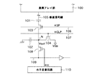
Q1=C1(Vrst−Vclp)
Q2=C2×Vclp
Vout=Vclp+C1(Vsig−Vrst)/(C1+C2)
上記の式から明らかなように、もし画素にトランジスタのしきい値電圧のばらつきがあったとしても、(Vsig−Vrst)によって固定パターンノイズを除去できる。
Q11=C11(Vrst1−Vclp)
Q12=C12×Vclp
Vout1=Vclp+C11(Vsig1−Vrst1)/(C11+C12)
Q13=C11(Vrst2−Vclp)
Q14=C13×Vclp
Vout2=Vclp+C11(Vsig2−Vrst2)/(C11+C13)
その結果、選択画素行n+1の画素にトランジスタのしきい値電圧のばらつきがあったとしても、(Vsig2−Vrst2)によって固定パターンノイズが除去される。ノードN3の電圧Vout2はそのままコンデンサ38に保持される。なお、コンデンサ35,38の容量C12,C13は略同一である。
Claims (2)
- 光電変換素子を含む画素が行列状に配置されてなる画素アレイ部と、各画素列に対応して配線された信号線と、前記信号線の各々に対して配設された複数のノイズ除去手段とを備えた固体撮像装置であって、
各々の前記ノイズ除去手段は、
前記信号線に一端が接続された第1のコンデンサと、
前記第1のコンデンサの他端に入力端が接続された第1のスイッチ手段と、
前記第1のスイッチ手段の出力端と基準電位との間に接続された第2のコンデンサと、
前記第1のスイッチ手段の入力端と前記第1のコンデンサの他端との接続ノードの電位を所定の電位にクランプするクランプ手段とを有し、
前記複数のノイズ除去手段は、前記第1のコンデンサを相互間で共有し、
前記信号線は、前記複数のノイズ除去手段の各々の前記第2のコンデンサが前記画素アレイ部から最も離れたノイズ除去手段が形成された領域まで等間隔で延在している
ことを特徴とする固体撮像装置。 - 光電変換素子を含む画素が行列状に配置されてなる画素アレイ部の各画素列ごとに配線された信号線を含む固体撮像装置であって、
前記信号線に一端が接続された第1のコンデンサと、
前記第1のコンデンサの他端に入力端が接続された第1のスイッチ手段と、
前記第1のスイッチ手段の出力端と基準電位との間に接続された第2のコンデンサと、
前記第1のスイッチ手段の出力端と前記第2のコンデンサとの接続ノードの電位を所定の電位にクランプする第1のクランプ手段と、
前記第1のスイッチ手段の出力端に接続され、前記画素により得られた信号を出力する第1の出力手段と、
前記第1のコンデンサの他端に入力端が接続された第2のスイッチ手段と、
前記第2のスイッチ手段の出力端と基準電位との間に接続された第3のコンデンサと、
前記第2のスイッチ手段の出力端と前記第3のコンデンサとの接続ノードの電位を所定の電位にクランプする第2のクランプ手段と
前記第2のスイッチ手段の出力端に接続され、前記画素により得られた信号を出力する第2の出力手段と、
を備えたことを特徴とする固体撮像装置。
Priority Applications (5)
| Application Number | Priority Date | Filing Date | Title |
|---|---|---|---|
| JP2003294938A JP4135594B2 (ja) | 2003-08-19 | 2003-08-19 | 固体撮像装置 |
| TW093123506A TWI248298B (en) | 2003-08-19 | 2004-08-05 | Solid-state imaging device |
| US10/914,352 US7432964B2 (en) | 2003-08-19 | 2004-08-09 | Solid-state imaging device with plural CDS circuits per column sharing a capacitor and/or clamping transistor |
| KR1020040064974A KR20050020658A (ko) | 2003-08-19 | 2004-08-18 | 고체 촬상 장치 |
| US12/217,072 US20090046187A1 (en) | 2003-08-19 | 2008-06-30 | Solid-state imaging device |
Applications Claiming Priority (1)
| Application Number | Priority Date | Filing Date | Title |
|---|---|---|---|
| JP2003294938A JP4135594B2 (ja) | 2003-08-19 | 2003-08-19 | 固体撮像装置 |
Publications (2)
| Publication Number | Publication Date |
|---|---|
| JP2005065069A JP2005065069A (ja) | 2005-03-10 |
| JP4135594B2 true JP4135594B2 (ja) | 2008-08-20 |
Family
ID=34191070
Family Applications (1)
| Application Number | Title | Priority Date | Filing Date |
|---|---|---|---|
| JP2003294938A Expired - Fee Related JP4135594B2 (ja) | 2003-08-19 | 2003-08-19 | 固体撮像装置 |
Country Status (4)
| Country | Link |
|---|---|
| US (2) | US7432964B2 (ja) |
| JP (1) | JP4135594B2 (ja) |
| KR (1) | KR20050020658A (ja) |
| TW (1) | TWI248298B (ja) |
Families Citing this family (11)
| Publication number | Priority date | Publication date | Assignee | Title |
|---|---|---|---|---|
| JP4135594B2 (ja) * | 2003-08-19 | 2008-08-20 | ソニー株式会社 | 固体撮像装置 |
| JP3814609B2 (ja) * | 2003-12-12 | 2006-08-30 | キヤノン株式会社 | 撮像装置、及び撮像装置の駆動方法 |
| JP5055469B2 (ja) * | 2006-08-04 | 2012-10-24 | 新世代株式会社 | イメージセンサ及びイメージセンサシステム |
| US7714903B2 (en) * | 2006-08-29 | 2010-05-11 | Zoran Corporation | Wide dynamic range image capturing system method and apparatus |
| JP5340643B2 (ja) * | 2008-06-03 | 2013-11-13 | オリンパス株式会社 | 固体撮像装置 |
| US20100271517A1 (en) * | 2009-04-24 | 2010-10-28 | Yannick De Wit | In-pixel correlated double sampling pixel |
| CN111164965B (zh) * | 2017-10-03 | 2023-07-18 | 索尼半导体解决方案公司 | 固态摄像器件和电子设备 |
| CN108391071B (zh) * | 2017-11-23 | 2020-04-14 | 南京邮电大学 | 一种采用二次相关双采样技术的spad阵列级读出电路 |
| US11089252B2 (en) * | 2019-01-23 | 2021-08-10 | STMicroelectronics (Grolles 2) SAS | Pixel with global shutter |
| KR102949116B1 (ko) * | 2019-09-27 | 2026-04-03 | 삼성전자주식회사 | 이미지 센서 및 그 동작 방법 |
| JP7765186B2 (ja) * | 2021-02-04 | 2025-11-06 | キヤノン株式会社 | 光電変換装置、電子機器および基板 |
Family Cites Families (10)
| Publication number | Priority date | Publication date | Assignee | Title |
|---|---|---|---|---|
| JP2913876B2 (ja) * | 1991-03-08 | 1999-06-28 | ソニー株式会社 | 固体撮像装置 |
| JPH04313268A (ja) * | 1991-04-10 | 1992-11-05 | Sony Corp | 固体撮像装置 |
| GB9619088D0 (en) * | 1996-09-12 | 1996-10-23 | Vlsi Vision Ltd | Ofset cancellation in array image sensors |
| JP4196029B2 (ja) | 1998-04-10 | 2008-12-17 | 株式会社ニコン | 撮像回路および撮像装置 |
| JP3559714B2 (ja) | 1998-09-02 | 2004-09-02 | キヤノン株式会社 | 撮像装置およびそれを用いた撮像システム |
| US6307195B1 (en) * | 1999-10-26 | 2001-10-23 | Eastman Kodak Company | Variable collection of blooming charge to extend dynamic range |
| US6710804B1 (en) * | 2000-01-18 | 2004-03-23 | Eastman Kodak Company | CMOS active pixel image sensor with extended dynamic range and sensitivity |
| JP3827146B2 (ja) | 2001-09-12 | 2006-09-27 | ソニー株式会社 | 固体撮像装置および固体撮像装置の駆動方法 |
| JP3899859B2 (ja) | 2001-07-11 | 2007-03-28 | ソニー株式会社 | 固体撮像素子およびその駆動方法、並びにカメラシステム |
| JP4135594B2 (ja) * | 2003-08-19 | 2008-08-20 | ソニー株式会社 | 固体撮像装置 |
-
2003
- 2003-08-19 JP JP2003294938A patent/JP4135594B2/ja not_active Expired - Fee Related
-
2004
- 2004-08-05 TW TW093123506A patent/TWI248298B/zh not_active IP Right Cessation
- 2004-08-09 US US10/914,352 patent/US7432964B2/en not_active Expired - Fee Related
- 2004-08-18 KR KR1020040064974A patent/KR20050020658A/ko not_active Ceased
-
2008
- 2008-06-30 US US12/217,072 patent/US20090046187A1/en not_active Abandoned
Also Published As
| Publication number | Publication date |
|---|---|
| KR20050020658A (ko) | 2005-03-04 |
| US20050040318A1 (en) | 2005-02-24 |
| TWI248298B (en) | 2006-01-21 |
| US7432964B2 (en) | 2008-10-07 |
| TW200509691A (en) | 2005-03-01 |
| JP2005065069A (ja) | 2005-03-10 |
| US20090046187A1 (en) | 2009-02-19 |
Similar Documents
| Publication | Publication Date | Title |
|---|---|---|
| US9661246B2 (en) | Solid state image pickup device having a capacitor structure made up of a plurality of capacitors | |
| KR101177140B1 (ko) | 고체 촬상 장치, 고체 촬상 장치의 구동 방법 및 촬상 장치 | |
| US20200328240A1 (en) | Imaging device and imaging system | |
| KR100834424B1 (ko) | 이미지 센서 | |
| KR101204571B1 (ko) | 고체 촬상 장치, 고체 촬상 장치의 구동 방법 및 카메라 | |
| CN101164334B (zh) | 光传感器、固体摄像装置和固体摄像装置的动作方法 | |
| JP5115937B2 (ja) | 固体撮像素子及びその製造方法 | |
| KR102749624B1 (ko) | 고체 촬상 소자 및 촬상 장치 | |
| US20090046187A1 (en) | Solid-state imaging device | |
| KR20230019213A (ko) | 촬상 장치 및 전자 기기 | |
| JP6413401B2 (ja) | 固体撮像素子 | |
| JP4807014B2 (ja) | 固体撮像装置、固体撮像装置の駆動方法および撮像装置 | |
| US8120688B2 (en) | Solid state imaging device | |
| JP6053321B2 (ja) | 固体撮像装置 | |
| JP4746962B2 (ja) | 固体撮像装置及び撮像システム | |
| JP6128776B2 (ja) | 固体撮像装置、撮像装置、および信号読み出し方法 | |
| JP5945463B2 (ja) | 固体撮像装置 | |
| JP2018152649A (ja) | 固体撮像装置及び固体撮像装置の駆動方法 |
Legal Events
| Date | Code | Title | Description |
|---|---|---|---|
| A621 | Written request for application examination |
Free format text: JAPANESE INTERMEDIATE CODE: A621 Effective date: 20050223 |
|
| A977 | Report on retrieval |
Free format text: JAPANESE INTERMEDIATE CODE: A971007 Effective date: 20080131 |
|
| A131 | Notification of reasons for refusal |
Free format text: JAPANESE INTERMEDIATE CODE: A131 Effective date: 20080212 |
|
| A521 | Request for written amendment filed |
Free format text: JAPANESE INTERMEDIATE CODE: A523 Effective date: 20080414 |
|
| TRDD | Decision of grant or rejection written | ||
| A01 | Written decision to grant a patent or to grant a registration (utility model) |
Free format text: JAPANESE INTERMEDIATE CODE: A01 Effective date: 20080513 |
|
| A01 | Written decision to grant a patent or to grant a registration (utility model) |
Free format text: JAPANESE INTERMEDIATE CODE: A01 |
|
| A61 | First payment of annual fees (during grant procedure) |
Free format text: JAPANESE INTERMEDIATE CODE: A61 Effective date: 20080526 |
|
| FPAY | Renewal fee payment (event date is renewal date of database) |
Free format text: PAYMENT UNTIL: 20110613 Year of fee payment: 3 |
|
| LAPS | Cancellation because of no payment of annual fees |