JP4200321B2 - 画像信号処理装置 - Google Patents
画像信号処理装置 Download PDFInfo
- Publication number
- JP4200321B2 JP4200321B2 JP2004152805A JP2004152805A JP4200321B2 JP 4200321 B2 JP4200321 B2 JP 4200321B2 JP 2004152805 A JP2004152805 A JP 2004152805A JP 2004152805 A JP2004152805 A JP 2004152805A JP 4200321 B2 JP4200321 B2 JP 4200321B2
- Authority
- JP
- Japan
- Prior art keywords
- data
- signal processing
- control unit
- transferred
- rom
- Prior art date
- Legal status (The legal status is an assumption and is not a legal conclusion. Google has not performed a legal analysis and makes no representation as to the accuracy of the status listed.)
- Expired - Fee Related
Links
Images


Classifications
-
- G—PHYSICS
- G09—EDUCATION; CRYPTOGRAPHY; DISPLAY; ADVERTISING; SEALS
- G09G—ARRANGEMENTS OR CIRCUITS FOR CONTROL OF INDICATING DEVICES USING STATIC MEANS TO PRESENT VARIABLE INFORMATION
- G09G3/00—Control arrangements or circuits, of interest only in connection with visual indicators other than cathode-ray tubes
- G09G3/20—Control arrangements or circuits, of interest only in connection with visual indicators other than cathode-ray tubes for presentation of an assembly of a number of characters, e.g. a page, by composing the assembly by combination of individual elements arranged in a matrix no fixed position being assigned to or needed to be assigned to the individual characters or partial characters
-
- G—PHYSICS
- G09—EDUCATION; CRYPTOGRAPHY; DISPLAY; ADVERTISING; SEALS
- G09G—ARRANGEMENTS OR CIRCUITS FOR CONTROL OF INDICATING DEVICES USING STATIC MEANS TO PRESENT VARIABLE INFORMATION
- G09G5/00—Control arrangements or circuits for visual indicators common to cathode-ray tube indicators and other visual indicators
- G09G5/003—Details of a display terminal, the details relating to the control arrangement of the display terminal and to the interfaces thereto
- G09G5/006—Details of the interface to the display terminal
-
- G—PHYSICS
- G09—EDUCATION; CRYPTOGRAPHY; DISPLAY; ADVERTISING; SEALS
- G09G—ARRANGEMENTS OR CIRCUITS FOR CONTROL OF INDICATING DEVICES USING STATIC MEANS TO PRESENT VARIABLE INFORMATION
- G09G5/00—Control arrangements or circuits for visual indicators common to cathode-ray tube indicators and other visual indicators
- G09G5/36—Control arrangements or circuits for visual indicators common to cathode-ray tube indicators and other visual indicators characterised by the display of a graphic pattern, e.g. using an all-points-addressable [APA] memory
- G09G5/39—Control of the bit-mapped memory
-
- G—PHYSICS
- G09—EDUCATION; CRYPTOGRAPHY; DISPLAY; ADVERTISING; SEALS
- G09G—ARRANGEMENTS OR CIRCUITS FOR CONTROL OF INDICATING DEVICES USING STATIC MEANS TO PRESENT VARIABLE INFORMATION
- G09G3/00—Control arrangements or circuits, of interest only in connection with visual indicators other than cathode-ray tubes
- G09G3/20—Control arrangements or circuits, of interest only in connection with visual indicators other than cathode-ray tubes for presentation of an assembly of a number of characters, e.g. a page, by composing the assembly by combination of individual elements arranged in a matrix no fixed position being assigned to or needed to be assigned to the individual characters or partial characters
- G09G3/22—Control arrangements or circuits, of interest only in connection with visual indicators other than cathode-ray tubes for presentation of an assembly of a number of characters, e.g. a page, by composing the assembly by combination of individual elements arranged in a matrix no fixed position being assigned to or needed to be assigned to the individual characters or partial characters using controlled light sources
- G09G3/28—Control arrangements or circuits, of interest only in connection with visual indicators other than cathode-ray tubes for presentation of an assembly of a number of characters, e.g. a page, by composing the assembly by combination of individual elements arranged in a matrix no fixed position being assigned to or needed to be assigned to the individual characters or partial characters using controlled light sources using luminous gas-discharge panels, e.g. plasma panels
- G09G3/288—Control arrangements or circuits, of interest only in connection with visual indicators other than cathode-ray tubes for presentation of an assembly of a number of characters, e.g. a page, by composing the assembly by combination of individual elements arranged in a matrix no fixed position being assigned to or needed to be assigned to the individual characters or partial characters using controlled light sources using luminous gas-discharge panels, e.g. plasma panels using AC panels
- G09G3/296—Driving circuits for producing the waveforms applied to the driving electrodes
Landscapes
- Engineering & Computer Science (AREA)
- Physics & Mathematics (AREA)
- Computer Hardware Design (AREA)
- General Physics & Mathematics (AREA)
- Theoretical Computer Science (AREA)
- Power Engineering (AREA)
- Plasma & Fusion (AREA)
- Control Of Indicators Other Than Cathode Ray Tubes (AREA)
- Controls And Circuits For Display Device (AREA)
- Control Of Gas Discharge Display Tubes (AREA)
Description
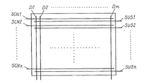
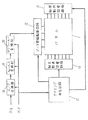
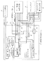
表示装置に映像出力データを出力する映像信号処理部およびこの映像信号処理部の動作を制御するデータを保持する制御部とを備えた半導体集積回路装置と、この半導体集積回路装置の外部に設けられかつ前記制御部に送るための制御データを保持するとともに前記制御部によりデータの読み出しが制御可能な外部メモリとを有し、
前記半導体集積回路装置の映像信号処理部は、前記映像信号処理部に入力される映像信号データの画質補正のための信号処理を行う画質補正回路と、前記画質補正回路の出力データに基づいてサブフィールド毎の信号を生成するサブフィールド変換回路と、前記外部メモリと前記制御部との間で転送されるとともに毎フィールド更新しなければならないデータである前記画質補正回路が要求するデータを保持するメモリと、前記外部メモリと前記制御部との間で転送されるとともに毎フィ一ルド更新する必要のないデータである前記サブフィールド変換回路が要求するデータを保持するメモリとを有し、
かつ前記半導体集積回路装置は、前記映像信号処理部からの映像出力データを出力するための端子として使用するとともに、制御部と外部メモリとの間でデータを転送するための端子として使用する入出力端子を備え、
かつ前記外部メモリと前記制御部との間で転送されるデータは、前記映像出力データの垂直ブランキング期間にデータを転送するように構成するとともに前記毎フィールド更新する必要のないデータは複数に分割して複数のフィールドに分けて転送するように構成したものである。
22 ROMアクセス制御回路
23 フラッシュROM
24a、25a SRAM
26 映像信号出力回路
27c 入出力端子
28、29 バッファ
31 セレクタ
32 I/O制御部
Claims (1)
- 1フィールド期間を複数のサブフィールドに分割するとともに、発光させるサブフィールドの組み合わせによって階調表示を行う表示装置の画像信号処理装置であって、
表示装置に映像出力データを出力する映像信号処理部およびこの映像信号処理部の動作を制御するデータを保持する制御部とを備えた半導体集積回路装置と、この半導体集積回路装置の外部に設けられかつ前記制御部に送るための制御データを保持するとともに前記制御部によりデータの読み出しが制御可能な外部メモリとを有し、
前記半導体集積回路装置の映像信号処理部は、前記映像信号処理部に入力される映像信号データの画質補正のための信号処理を行う画質補正回路と、前記画質補正回路の出力データに基づいてサブフィールド毎の信号を生成するサブフィールド変換回路と、前記外部メモリと前記制御部との間で転送されるとともに毎フィールド更新しなければならないデータである前記画質補正回路が要求するデータを保持するメモリと、前記外部メモリと前記制御部との間で転送されるとともに毎フィ一ルド更新する必要のないデータである前記サブフィールド変換回路が要求するデータを保持するメモリとを有し、
かつ前記半導体集積回路装置は、前記映像信号処理部からの映像出力データを出力するための端子として使用するとともに、制御部と外部メモリとの間でデータを転送するための端子として使用する入出力端子を備え、
かつ前記外部メモリと前記制御部との間で転送されるデータは、前記映像出力データの垂直ブランキング期間にデータを転送するように構成するとともに前記毎フィールド更新する必要のないデータは複数に分割して複数のフィールドに分けて転送するように構成したことを特徴とする画像信号処理装置。
Priority Applications (7)
| Application Number | Priority Date | Filing Date | Title |
|---|---|---|---|
| JP2004152805A JP4200321B2 (ja) | 2004-05-24 | 2004-05-24 | 画像信号処理装置 |
| CNB2005800005377A CN100476913C (zh) | 2004-05-24 | 2005-05-24 | 图像信号处理装置 |
| KR1020067001097A KR20060032639A (ko) | 2004-05-24 | 2005-05-24 | 화상 신호 처리 장치 |
| KR1020077020306A KR100868128B1 (ko) | 2004-05-24 | 2005-05-24 | 화상 신호 처리 장치 |
| KR1020087005803A KR20080028515A (ko) | 2004-05-24 | 2005-05-24 | 화상 신호 처리 장치 |
| PCT/JP2005/009833 WO2005114625A1 (ja) | 2004-05-24 | 2005-05-24 | 画像信号処理装置 |
| US10/563,509 US20060165278A1 (en) | 2004-05-24 | 2005-05-24 | Image signal processing device |
Applications Claiming Priority (1)
| Application Number | Priority Date | Filing Date | Title |
|---|---|---|---|
| JP2004152805A JP4200321B2 (ja) | 2004-05-24 | 2004-05-24 | 画像信号処理装置 |
Publications (2)
| Publication Number | Publication Date |
|---|---|
| JP2005338123A JP2005338123A (ja) | 2005-12-08 |
| JP4200321B2 true JP4200321B2 (ja) | 2008-12-24 |
Family
ID=35428585
Family Applications (1)
| Application Number | Title | Priority Date | Filing Date |
|---|---|---|---|
| JP2004152805A Expired - Fee Related JP4200321B2 (ja) | 2004-05-24 | 2004-05-24 | 画像信号処理装置 |
Country Status (5)
| Country | Link |
|---|---|
| US (1) | US20060165278A1 (ja) |
| JP (1) | JP4200321B2 (ja) |
| KR (3) | KR100868128B1 (ja) |
| CN (1) | CN100476913C (ja) |
| WO (1) | WO2005114625A1 (ja) |
Families Citing this family (4)
| Publication number | Priority date | Publication date | Assignee | Title |
|---|---|---|---|---|
| JP2005331559A (ja) * | 2004-05-18 | 2005-12-02 | Matsushita Electric Ind Co Ltd | 画像信号処理装置 |
| JP2009239899A (ja) * | 2008-03-04 | 2009-10-15 | Seiko Epson Corp | 画像処理回路及びそれを含む電子機器 |
| WO2012001886A1 (ja) * | 2010-06-28 | 2012-01-05 | パナソニック株式会社 | プラズマディスプレイパネル用集積回路、アクセス制御方法及びプラズマディスプレイシステム |
| US11978372B1 (en) * | 2023-05-16 | 2024-05-07 | Qualcomm Incorporated | Synchronized dual eye variable refresh rate update for VR display |
Family Cites Families (8)
| Publication number | Priority date | Publication date | Assignee | Title |
|---|---|---|---|---|
| JPH03219291A (ja) * | 1989-11-09 | 1991-09-26 | Matsushita Electric Ind Co Ltd | 大画面画像表示法 |
| JPH104516A (ja) * | 1996-06-18 | 1998-01-06 | Canon Inc | 情報処理システムおよび情報処理方法 |
| WO1998044479A1 (en) * | 1997-03-31 | 1998-10-08 | Matsushita Electric Industrial Co., Ltd. | Dynamic image display method and device therefor |
| JP3733773B2 (ja) * | 1999-02-22 | 2006-01-11 | 松下電器産業株式会社 | Ac型プラズマディスプレイパネルの駆動方法 |
| JP2001092436A (ja) * | 1999-09-24 | 2001-04-06 | Olympus Optical Co Ltd | 画像処理装置 |
| KR100364705B1 (ko) * | 2000-05-18 | 2002-12-16 | 엘지전자 주식회사 | 동기유도 전동기의 회전자 |
| JP4267299B2 (ja) * | 2001-11-19 | 2009-05-27 | パナソニック株式会社 | 表示制御装置、画像表示装置および制御データ転送方法 |
| KR100438918B1 (ko) * | 2001-12-08 | 2004-07-03 | 엘지전자 주식회사 | 플라즈마 디스플레이 패널의 구동방법 및 장치 |
-
2004
- 2004-05-24 JP JP2004152805A patent/JP4200321B2/ja not_active Expired - Fee Related
-
2005
- 2005-05-24 KR KR1020077020306A patent/KR100868128B1/ko not_active Expired - Fee Related
- 2005-05-24 KR KR1020087005803A patent/KR20080028515A/ko not_active Withdrawn
- 2005-05-24 CN CNB2005800005377A patent/CN100476913C/zh not_active Expired - Fee Related
- 2005-05-24 KR KR1020067001097A patent/KR20060032639A/ko not_active Ceased
- 2005-05-24 WO PCT/JP2005/009833 patent/WO2005114625A1/ja not_active Ceased
- 2005-05-24 US US10/563,509 patent/US20060165278A1/en not_active Abandoned
Also Published As
| Publication number | Publication date |
|---|---|
| KR100868128B1 (ko) | 2008-11-10 |
| KR20080028515A (ko) | 2008-03-31 |
| CN1806271A (zh) | 2006-07-19 |
| WO2005114625A1 (ja) | 2005-12-01 |
| KR20060032639A (ko) | 2006-04-17 |
| KR20070096061A (ko) | 2007-10-01 |
| CN100476913C (zh) | 2009-04-08 |
| JP2005338123A (ja) | 2005-12-08 |
| US20060165278A1 (en) | 2006-07-27 |
Similar Documents
| Publication | Publication Date | Title |
|---|---|---|
| KR100533727B1 (ko) | 플라즈마 디스플레이 패널의 구동 장치 | |
| JP2005107533A (ja) | プラズマディスプレイパネルの駆動装置及び駆動方法 | |
| JP4200321B2 (ja) | 画像信号処理装置 | |
| KR100573119B1 (ko) | 패널구동장치 | |
| JP2005331559A (ja) | 画像信号処理装置 | |
| JP2005331560A (ja) | 画像信号処理装置 | |
| US6911783B2 (en) | Drive method for plasma display panel and drive device for plasma display panel | |
| JP2008070488A (ja) | ガス放電表示装置 | |
| JPWO2008087805A1 (ja) | プラズマディスプレイパネルの駆動方法およびプラズマディスプレイ装置 | |
| JP5011615B2 (ja) | プラズマディスプレイ装置 | |
| JP2005157364A (ja) | プラズマディスプレイパネルの駆動方法及び装置 | |
| JP2009192652A (ja) | プラズマディスプレイ装置 | |
| US8054246B2 (en) | Plasma display apparatus comprising data driver having data arranging unit | |
| KR100237420B1 (ko) | 플라즈마 디스플레이장치 및 패널구조 | |
| US20050104813A1 (en) | Plasma display panel having a driving apparatus and method for displaying pictures | |
| JP2002202753A (ja) | プラズマディスプレイパネルの駆動方法およびプラズマディスプレイパネルの駆動装置 | |
| JP2003058102A (ja) | マトリクス表示装置及びその駆動方法 | |
| KR100342832B1 (ko) | 플라즈마 디스플레이 패널의 구동장치 | |
| KR100492950B1 (ko) | 에이씨피디피구동시스템 | |
| JP2005084364A (ja) | プラズマディスプレイ装置 | |
| KR100514259B1 (ko) | 플라즈마 디스플레이 패널의 구동 장치 및 방법 | |
| US20050093778A1 (en) | Panel driving method and apparatus | |
| JP2005301282A (ja) | プラズマディスプレイパネルの駆動装置及びその駆動方法 | |
| KR100462786B1 (ko) | 노이즈 저감을 위한 스캔 드라이버 집적회로와, 그구동방법, 및 이를 구비하는 플라즈마 디스플레이 패널의구동장치 | |
| JP2004126453A (ja) | 表示装置 |
Legal Events
| Date | Code | Title | Description |
|---|---|---|---|
| A621 | Written request for application examination |
Free format text: JAPANESE INTERMEDIATE CODE: A621 Effective date: 20070509 |
|
| RD01 | Notification of change of attorney |
Free format text: JAPANESE INTERMEDIATE CODE: A7421 Effective date: 20070613 |
|
| A131 | Notification of reasons for refusal |
Free format text: JAPANESE INTERMEDIATE CODE: A131 Effective date: 20080311 |
|
| A521 | Written amendment |
Free format text: JAPANESE INTERMEDIATE CODE: A523 Effective date: 20080508 |
|
| A02 | Decision of refusal |
Free format text: JAPANESE INTERMEDIATE CODE: A02 Effective date: 20080610 |
|
| A521 | Written amendment |
Free format text: JAPANESE INTERMEDIATE CODE: A523 Effective date: 20080710 |
|
| A911 | Transfer to examiner for re-examination before appeal (zenchi) |
Free format text: JAPANESE INTERMEDIATE CODE: A911 Effective date: 20080815 |
|
| TRDD | Decision of grant or rejection written | ||
| A01 | Written decision to grant a patent or to grant a registration (utility model) |
Free format text: JAPANESE INTERMEDIATE CODE: A01 Effective date: 20080909 |
|
| A01 | Written decision to grant a patent or to grant a registration (utility model) |
Free format text: JAPANESE INTERMEDIATE CODE: A01 |
|
| A61 | First payment of annual fees (during grant procedure) |
Free format text: JAPANESE INTERMEDIATE CODE: A61 Effective date: 20080922 |
|
| FPAY | Renewal fee payment (event date is renewal date of database) |
Free format text: PAYMENT UNTIL: 20111017 Year of fee payment: 3 |
|
| FPAY | Renewal fee payment (event date is renewal date of database) |
Free format text: PAYMENT UNTIL: 20121017 Year of fee payment: 4 |
|
| FPAY | Renewal fee payment (event date is renewal date of database) |
Free format text: PAYMENT UNTIL: 20131017 Year of fee payment: 5 |
|
| LAPS | Cancellation because of no payment of annual fees |