JP4236594B2 - 光学装置用モジュール及び光学装置用モジュールの製造方法 - Google Patents
光学装置用モジュール及び光学装置用モジュールの製造方法 Download PDFInfo
- Publication number
- JP4236594B2 JP4236594B2 JP2004019006A JP2004019006A JP4236594B2 JP 4236594 B2 JP4236594 B2 JP 4236594B2 JP 2004019006 A JP2004019006 A JP 2004019006A JP 2004019006 A JP2004019006 A JP 2004019006A JP 4236594 B2 JP4236594 B2 JP 4236594B2
- Authority
- JP
- Japan
- Prior art keywords
- solid
- state imaging
- imaging device
- optical path
- optical
- Prior art date
- Legal status (The legal status is an assumption and is not a legal conclusion. Google has not performed a legal analysis and makes no representation as to the accuracy of the status listed.)
- Expired - Fee Related
Links
Images






Classifications
-
- G—PHYSICS
- G03—PHOTOGRAPHY; CINEMATOGRAPHY; ANALOGOUS TECHNIQUES USING WAVES OTHER THAN OPTICAL WAVES; ELECTROGRAPHY; HOLOGRAPHY
- G03B—APPARATUS OR ARRANGEMENTS FOR TAKING PHOTOGRAPHS OR FOR PROJECTING OR VIEWING THEM; APPARATUS OR ARRANGEMENTS EMPLOYING ANALOGOUS TECHNIQUES USING WAVES OTHER THAN OPTICAL WAVES; ACCESSORIES THEREFOR
- G03B30/00—Camera modules comprising integrated lens units and imaging units, specially adapted for being embedded in other devices, e.g. mobile phones or vehicles
-
- G—PHYSICS
- G02—OPTICS
- G02B—OPTICAL ELEMENTS, SYSTEMS OR APPARATUS
- G02B13/00—Optical objectives specially designed for the purposes specified below
- G02B13/001—Miniaturised objectives for electronic devices, e.g. portable telephones, webcams, PDAs, small digital cameras
-
- G—PHYSICS
- G02—OPTICS
- G02B—OPTICAL ELEMENTS, SYSTEMS OR APPARATUS
- G02B7/00—Mountings, adjusting means, or light-tight connections, for optical elements
- G02B7/02—Mountings, adjusting means, or light-tight connections, for optical elements for lenses
-
- H—ELECTRICITY
- H04—ELECTRIC COMMUNICATION TECHNIQUE
- H04N—PICTORIAL COMMUNICATION, e.g. TELEVISION
- H04N23/00—Cameras or camera modules comprising electronic image sensors; Control thereof
- H04N23/50—Constructional details
- H04N23/54—Mounting of pick-up tubes, electronic image sensors, deviation or focusing coils
-
- H—ELECTRICITY
- H04—ELECTRIC COMMUNICATION TECHNIQUE
- H04N—PICTORIAL COMMUNICATION, e.g. TELEVISION
- H04N23/00—Cameras or camera modules comprising electronic image sensors; Control thereof
- H04N23/50—Constructional details
- H04N23/55—Optical parts specially adapted for electronic image sensors; Mounting thereof
-
- H—ELECTRICITY
- H10—SEMICONDUCTOR DEVICES; ELECTRIC SOLID-STATE DEVICES NOT OTHERWISE PROVIDED FOR
- H10F—INORGANIC SEMICONDUCTOR DEVICES SENSITIVE TO INFRARED RADIATION, LIGHT, ELECTROMAGNETIC RADIATION OF SHORTER WAVELENGTH OR CORPUSCULAR RADIATION
- H10F39/00—Integrated devices, or assemblies of multiple devices, comprising at least one element covered by group H10F30/00, e.g. radiation detectors comprising photodiode arrays
- H10F39/80—Constructional details of image sensors
- H10F39/804—Containers or encapsulations
-
- H—ELECTRICITY
- H10—SEMICONDUCTOR DEVICES; ELECTRIC SOLID-STATE DEVICES NOT OTHERWISE PROVIDED FOR
- H10F—INORGANIC SEMICONDUCTOR DEVICES SENSITIVE TO INFRARED RADIATION, LIGHT, ELECTROMAGNETIC RADIATION OF SHORTER WAVELENGTH OR CORPUSCULAR RADIATION
- H10F39/00—Integrated devices, or assemblies of multiple devices, comprising at least one element covered by group H10F30/00, e.g. radiation detectors comprising photodiode arrays
- H10F39/80—Constructional details of image sensors
- H10F39/806—Optical elements or arrangements associated with the image sensors
-
- H—ELECTRICITY
- H10—SEMICONDUCTOR DEVICES; ELECTRIC SOLID-STATE DEVICES NOT OTHERWISE PROVIDED FOR
- H10F—INORGANIC SEMICONDUCTOR DEVICES SENSITIVE TO INFRARED RADIATION, LIGHT, ELECTROMAGNETIC RADIATION OF SHORTER WAVELENGTH OR CORPUSCULAR RADIATION
- H10F77/00—Constructional details of devices covered by this subclass
- H10F77/40—Optical elements or arrangements
- H10F77/407—Optical elements or arrangements indirectly associated with the devices
-
- H—ELECTRICITY
- H10—SEMICONDUCTOR DEVICES; ELECTRIC SOLID-STATE DEVICES NOT OTHERWISE PROVIDED FOR
- H10F—INORGANIC SEMICONDUCTOR DEVICES SENSITIVE TO INFRARED RADIATION, LIGHT, ELECTROMAGNETIC RADIATION OF SHORTER WAVELENGTH OR CORPUSCULAR RADIATION
- H10F77/00—Constructional details of devices covered by this subclass
- H10F77/50—Encapsulations or containers
-
- H—ELECTRICITY
- H10—SEMICONDUCTOR DEVICES; ELECTRIC SOLID-STATE DEVICES NOT OTHERWISE PROVIDED FOR
- H10W—GENERIC PACKAGES, INTERCONNECTIONS, CONNECTORS OR OTHER CONSTRUCTIONAL DETAILS OF DEVICES COVERED BY CLASS H10
- H10W72/00—Interconnections or connectors in packages
- H10W72/851—Dispositions of multiple connectors or interconnections
- H10W72/874—On different surfaces
- H10W72/884—Die-attach connectors and bond wires
Landscapes
- Physics & Mathematics (AREA)
- General Physics & Mathematics (AREA)
- Engineering & Computer Science (AREA)
- Multimedia (AREA)
- Signal Processing (AREA)
- Optics & Photonics (AREA)
- Solid State Image Pick-Up Elements (AREA)
- Transforming Light Signals Into Electric Signals (AREA)
Description
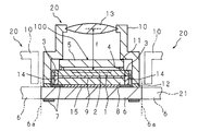
更に本発明にあっては、固体撮像素子、透光性蓋部、及び画像処理装置が光路画定器に収納され、光路画定器の内部と透光性蓋部とが結合部にて結合される。また、光路画定器の他端部と、配線基板の画像処理装置が接着されている面(以下、配線基板の装置接着面という)とが対向配置され、光路画定器の他端部と配線基板の装置接着面との間に、調整部が設けられる。調整部は、光路画定器の他端部と配線基板の装置接着面との間の距離を自動的に調整する。
更にまた、本発明の光学装置用モジュール及び光学装置用モジュールの製造方法によれば、配線基板の板厚にバラツキがあっても、又は配線基板が変形しても、配線基板の板厚のバラツキ又は配線基板の変形等に応じて、調整部が、光路画定器の他端部と配線基板の装置接着面との間の距離を自動的に調整する。このため、透光性蓋部を基準にレンズと固体撮像素子との光学距離をレンズの焦点距離に精密に一致させることができ、レンズの光軸と固体撮像素子の垂直軸とを一致させることができ、しかも、配線基板の板厚のバラツキ又は配線基板の変形等によって光学装置用モジュールに生じるストレスを低減することができる。
2 有効画素領域
3 貫通電極
4 接着部
5 透光性蓋部
6 配線基板
7 導体配線
8 DSP(画像処理装置)
9 接着部
10 光路画定器
11 結合部
12 調整部
13 レンズ
14 貫通電極
15 接着部
20 光学装置用モジュール
Claims (8)
- 一面に有効画素領域を有する固体撮像素子と、前記有効画素領域への光路を画定する光路画定器とを備える光学装置用モジュールにおいて、
前記固体撮像素子を貫通する貫通電極と、
前記有効画素領域に対向して配置される透光性蓋部を前記固体撮像素子に接着する接着部と、
前記透光性蓋部及び前記光路画定器を結合する結合部と
を備え、
前記光路画定器は筒状であって、一端部が、前記有効画素領域に対向して配置されるレンズを保持するようにしてあり、
前記固体撮像素子は配線基板に接着された画像処理装置の平面部に接着されており、
前記固体撮像素子、前記透光性蓋部、及び前記画像処理装置は前記光路画定器に収納されており、
前記結合部は前記透光性蓋部及び前記光路画定器の内部を結合しており、
前記光路画定器の他端部と前記配線基板の前記画像処理装置が接着されている面とが対向配置されており、
前記他端部と前記面との間に空隙を設けることによって、前記間の距離を自動的に調整する調整部を設けてあることを特徴とする光学装置用モジュール。 - 前記結合部は前記透光性蓋部及び前記光路画定器を接着していることを特徴とする請求項1に記載の光学装置用モジュール。
- 前記透光性蓋部は前記固体撮像素子の前記一面の平面寸法より小さい平面寸法を有することを特徴とする請求項1又は2に記載の光学装置用モジュール。
- 前記接着部は感光性接着剤を含むことを特徴とする請求項1乃至3の何れかひとつに記載の光学装置用モジュール。
- 前記有効画素領域及び透光性蓋部の間には空間が形成され、前記接着部は前記一面における有効画素領域の外周部に形成されていることを特徴とする請求項1乃至4の何れかひとつに記載の光学装置用モジュール。
- 前記接着部は前記外周部を密封する構成としてあることを特徴とする請求項5に記載の光学装置用モジュール。
- 前記貫通電極と前記画像処理装置を貫通する貫通電極とが接続されていることを特徴とする請求項1乃至6の何れかひとつに記載の光学装置用モジュール。
- 一面に有効画素領域を有する固体撮像素子と、筒状であって、一端部が、前記有効画素領域に対向して配置されるレンズを保持し、前記有効画素領域への光路を画定する光路画定器とを備える光学装置用モジュールの製造方法において、
前記固体撮像素子に貫通電極を形成する工程と、
前記有効画素領域に対向して配置した透光性蓋部を前記固体撮像素子に接着する工程と、
前記固体撮像素子を、配線基板に接着された画像処理装置の平面部に接着する工程と、
前記光路画定器の他端部と前記配線基板の前記画像処理装置が接着されている面とを対向配置し、前記固体撮像素子、前記透光性蓋部、及び前記画像処理装置を前記光路画定器に収納し、前記透光性蓋部に前記光路画定器の内部を結合し、前記光路画定器の前記他端部と前記配線基板との間に空隙を設けることによって、前記間の距離を自動的に調整する調整部を設ける工程と
を備えることを特徴とする光学装置用モジュールの製造方法。
Priority Applications (5)
| Application Number | Priority Date | Filing Date | Title |
|---|---|---|---|
| JP2004019006A JP4236594B2 (ja) | 2004-01-27 | 2004-01-27 | 光学装置用モジュール及び光学装置用モジュールの製造方法 |
| US11/039,813 US7265916B2 (en) | 2004-01-27 | 2005-01-24 | Module for optical devices, and manufacturing method of module for optical devices |
| KR1020050006917A KR100822968B1 (ko) | 2004-01-27 | 2005-01-26 | 광학 장치용 모듈 및 광학 장치용 모듈의 제조 방법 |
| TW094102238A TWI270707B (en) | 2004-01-27 | 2005-01-26 | Module for optical devices, and manufacturing method of module for optical devices |
| CNB2005100063302A CN1324340C (zh) | 2004-01-27 | 2005-01-26 | 光学装置用模块和光学装置用模块的制造方法 |
Applications Claiming Priority (1)
| Application Number | Priority Date | Filing Date | Title |
|---|---|---|---|
| JP2004019006A JP4236594B2 (ja) | 2004-01-27 | 2004-01-27 | 光学装置用モジュール及び光学装置用モジュールの製造方法 |
Publications (2)
| Publication Number | Publication Date |
|---|---|
| JP2005216970A JP2005216970A (ja) | 2005-08-11 |
| JP4236594B2 true JP4236594B2 (ja) | 2009-03-11 |
Family
ID=34792560
Family Applications (1)
| Application Number | Title | Priority Date | Filing Date |
|---|---|---|---|
| JP2004019006A Expired - Fee Related JP4236594B2 (ja) | 2004-01-27 | 2004-01-27 | 光学装置用モジュール及び光学装置用モジュールの製造方法 |
Country Status (5)
| Country | Link |
|---|---|
| US (1) | US7265916B2 (ja) |
| JP (1) | JP4236594B2 (ja) |
| KR (1) | KR100822968B1 (ja) |
| CN (1) | CN1324340C (ja) |
| TW (1) | TWI270707B (ja) |
Families Citing this family (39)
| Publication number | Priority date | Publication date | Assignee | Title |
|---|---|---|---|---|
| US7368695B2 (en) * | 2004-05-03 | 2008-05-06 | Tessera, Inc. | Image sensor package and fabrication method |
| JP3830497B2 (ja) | 2004-06-11 | 2006-10-04 | シャープ株式会社 | 半導体ウエハの製造方法及び半導体装置の製造方法 |
| JP2006276463A (ja) * | 2005-03-29 | 2006-10-12 | Sharp Corp | 光学装置用モジュール及び光学装置用モジュールの製造方法 |
| JP2007007227A (ja) * | 2005-07-01 | 2007-01-18 | Pentax Corp | 電子内視鏡用撮像装置 |
| DE102005061206B4 (de) | 2005-09-30 | 2019-10-17 | Osram Opto Semiconductors Gmbh | Verwendung einer Detektoranordnung als Umgebungslichtsensor |
| CN100470847C (zh) * | 2006-01-13 | 2009-03-18 | 崴强科技股份有限公司 | 影像感测芯片封装装置 |
| US7822338B2 (en) * | 2006-01-20 | 2010-10-26 | Sony Ericsson Mobile Communications Ab | Camera for electronic device |
| JP2007214438A (ja) * | 2006-02-10 | 2007-08-23 | Dainippon Printing Co Ltd | センサーパッケージ |
| JP2007214441A (ja) * | 2006-02-10 | 2007-08-23 | Dainippon Printing Co Ltd | 複合センサーパッケージ |
| CN100454508C (zh) * | 2006-03-01 | 2009-01-21 | 旺宏电子股份有限公司 | 制造影像撷取组件及照相模块的方法 |
| KR101294419B1 (ko) * | 2006-03-10 | 2013-08-08 | 엘지이노텍 주식회사 | 카메라 모듈 및 그 제조 방법 |
| JP4950542B2 (ja) * | 2006-04-07 | 2012-06-13 | 岩手東芝エレクトロニクス株式会社 | 固体撮像装置およびその製造方法 |
| JP4160083B2 (ja) * | 2006-04-11 | 2008-10-01 | シャープ株式会社 | 光学装置用モジュール及び光学装置用モジュールの製造方法 |
| KR20070105723A (ko) * | 2006-04-27 | 2007-10-31 | 삼성전기주식회사 | 카메라 모듈 패키지 |
| JP4908150B2 (ja) * | 2006-10-18 | 2012-04-04 | 浜松ホトニクス株式会社 | 撮像装置の保持構造及び撮像装置 |
| CN101165523B (zh) * | 2006-10-20 | 2010-05-26 | 鸿富锦精密工业(深圳)有限公司 | 影像感测模组封装结构 |
| CN101193507B (zh) * | 2006-12-01 | 2011-07-27 | 深圳富泰宏精密工业有限公司 | 具有平板视窗镜片的壳体及其制造方法 |
| US8456560B2 (en) * | 2007-01-26 | 2013-06-04 | Digitaloptics Corporation | Wafer level camera module and method of manufacture |
| JP4340698B2 (ja) * | 2007-04-27 | 2009-10-07 | シャープ株式会社 | 光学ユニットおよびそれを備えた固体撮像装置並びに電子機器 |
| CN100561736C (zh) * | 2007-05-25 | 2009-11-18 | 鸿富锦精密工业(深圳)有限公司 | 影像感测器封装结构及其应用的成像模组 |
| JPWO2008153082A1 (ja) | 2007-06-12 | 2010-08-26 | 住友ベークライト株式会社 | 樹脂組成物、埋め込み材、絶縁層および半導体装置 |
| JP4799543B2 (ja) * | 2007-12-27 | 2011-10-26 | 株式会社東芝 | 半導体パッケージ及びカメラモジュール |
| US9419032B2 (en) | 2009-08-14 | 2016-08-16 | Nanchang O-Film Optoelectronics Technology Ltd | Wafer level camera module with molded housing and method of manufacturing |
| WO2011111248A1 (ja) * | 2010-03-10 | 2011-09-15 | Smk株式会社 | カメラモジュール |
| KR101143938B1 (ko) * | 2010-04-22 | 2012-05-15 | 주식회사 지멤스 | 이미지센서 모듈, 이를 포함하는 영상 장치 및 그 제조방법 |
| JP6021618B2 (ja) * | 2012-12-05 | 2016-11-09 | オリンパス株式会社 | 撮像装置、内視鏡及び撮像装置の製造方法 |
| US9276030B2 (en) * | 2013-03-15 | 2016-03-01 | Sensors Unlimited, Inc. | Read out integrated circuit input/output routing on permanent carrier |
| US9000344B2 (en) * | 2013-03-15 | 2015-04-07 | Sensors Unlimited, Inc. | Focal plane array periphery through-vias for read out integrated circuit |
| JP6217907B2 (ja) * | 2013-08-02 | 2017-10-25 | 住友電気工業株式会社 | 光センサ装置およびスペクトルイメージング撮像システム |
| US9640709B2 (en) | 2013-09-10 | 2017-05-02 | Heptagon Micro Optics Pte. Ltd. | Compact opto-electronic modules and fabrication methods for such modules |
| JP6300029B2 (ja) * | 2014-01-27 | 2018-03-28 | ソニー株式会社 | 撮像素子、製造装置、製造方法 |
| SG11201606706WA (en) | 2014-02-18 | 2016-09-29 | Heptagon Micro Optics Pte Ltd | Optical modules including customizable spacers for focal length adjustment and/or reduction of tilt, and fabrication of the optical modules |
| US10890733B2 (en) * | 2015-04-06 | 2021-01-12 | Ams Sensors Singapore Pte. Ltd. | Image sensor module with auto focus control |
| GB2537628B (en) | 2015-04-21 | 2019-05-15 | Qioptiq Ltd | Low stress mounting configuration for optical component |
| US20170047362A1 (en) * | 2015-08-13 | 2017-02-16 | Heptagon Micro Optics Pte. Ltd. | Optoelectronic module with customizable spacers |
| US10466501B2 (en) * | 2016-05-26 | 2019-11-05 | Ams Sensors Singapore Pte. Ltd. | Optoelectronic modules including an optical system tilted with respect to a focal plane |
| CN112118373B (zh) * | 2019-06-21 | 2021-08-06 | 致伸科技股份有限公司 | 微型化影像采集模块及其制作方法 |
| EP4160666A4 (en) * | 2020-05-28 | 2023-10-25 | Sony Semiconductor Solutions Corporation | SOLID STATE IMAGING APPARATUS AND ELECTRONIC DEVICE |
| KR102897027B1 (ko) * | 2021-04-19 | 2025-12-05 | 청두 신센스 테크놀로지 씨오., 엘티디. | 인터페이스 시스템을 갖는 이벤트 구동 집적 회로 |
Family Cites Families (9)
| Publication number | Priority date | Publication date | Assignee | Title |
|---|---|---|---|---|
| US6437925B1 (en) * | 1998-06-30 | 2002-08-20 | Olympus Optical Co., Ltd. | Optical apparatus |
| JP2001016486A (ja) * | 1999-06-25 | 2001-01-19 | Toshiba Corp | 固体撮像素子モジュール |
| JP2001250930A (ja) * | 2000-03-03 | 2001-09-14 | Olympus Optical Co Ltd | 小型撮像モジュール |
| JP2002182270A (ja) | 2000-12-15 | 2002-06-26 | Toshiba Corp | カメラモジュール及びその製造方法 |
| JP3540281B2 (ja) * | 2001-02-02 | 2004-07-07 | シャープ株式会社 | 撮像装置 |
| JP2002231918A (ja) * | 2001-02-06 | 2002-08-16 | Olympus Optical Co Ltd | 固体撮像装置及びその製造方法 |
| JP4000507B2 (ja) | 2001-10-04 | 2007-10-31 | ソニー株式会社 | 固体撮像装置の製造方法 |
| US6949808B2 (en) | 2001-11-30 | 2005-09-27 | Matsushita Electric Industrial Co., Ltd. | Solid-state imaging apparatus and manufacturing method thereof |
| EP1348990B1 (en) | 2002-03-25 | 2006-01-11 | Konica Corporation | Objective composed of three lenses |
-
2004
- 2004-01-27 JP JP2004019006A patent/JP4236594B2/ja not_active Expired - Fee Related
-
2005
- 2005-01-24 US US11/039,813 patent/US7265916B2/en not_active Expired - Fee Related
- 2005-01-26 CN CNB2005100063302A patent/CN1324340C/zh not_active Expired - Fee Related
- 2005-01-26 TW TW094102238A patent/TWI270707B/zh not_active IP Right Cessation
- 2005-01-26 KR KR1020050006917A patent/KR100822968B1/ko not_active Expired - Fee Related
Also Published As
| Publication number | Publication date |
|---|---|
| CN1648707A (zh) | 2005-08-03 |
| TWI270707B (en) | 2007-01-11 |
| CN1324340C (zh) | 2007-07-04 |
| US20050163016A1 (en) | 2005-07-28 |
| JP2005216970A (ja) | 2005-08-11 |
| KR20050077267A (ko) | 2005-08-01 |
| TW200537152A (en) | 2005-11-16 |
| US7265916B2 (en) | 2007-09-04 |
| KR100822968B1 (ko) | 2008-04-17 |
Similar Documents
| Publication | Publication Date | Title |
|---|---|---|
| JP4236594B2 (ja) | 光学装置用モジュール及び光学装置用モジュールの製造方法 | |
| EP1462839B1 (en) | Module for optical image capturing device comprising objective lens and image sensor | |
| CN100533727C (zh) | 光学装置用模块和光学装置用模块的制造方法 | |
| CN100534148C (zh) | 摄像装置和便携式终端设备以及摄像装置的制造方法 | |
| CN100433303C (zh) | 半导体器件、光学器件模块以及半导体器件的制造方法 | |
| US7593636B2 (en) | Pin referenced image sensor to reduce tilt in a camera module | |
| KR100604190B1 (ko) | 고체촬상장치, 반도체 웨이퍼, 광학장치용 모듈,고체촬상장치의 제조방법, 및 광학장치용 모듈의 제조방법 | |
| US7083999B2 (en) | Optical device, method of manufacturing the same, optical module, circuit board and electronic instrument | |
| JP2001351997A (ja) | 受光センサーの実装構造体およびその使用方法 | |
| KR20090115101A (ko) | 고체 촬상 장치 및 그의 제조 방법 | |
| JP2002329850A (ja) | チップサイズパッケージおよびその製造方法 | |
| CN101569178A (zh) | 固态成像设备及其制造方法 | |
| KR20200063102A (ko) | 촬영 어셈블리 및 이의 패키징 방법, 렌즈 모듈, 전자 기기 | |
| JP2004242166A (ja) | 光モジュール及びその製造方法並びに電子機器 | |
| JP2005317745A (ja) | 固体撮像装置およびその製造方法 | |
| JP4145619B2 (ja) | 光モジュール及びその製造方法、回路基板並びに電子機器 | |
| US20090315130A1 (en) | Solid-state imaging apparatus and method for manufacturing the same | |
| JP4138436B2 (ja) | 光モジュール、回路基板及び電子機器 |
Legal Events
| Date | Code | Title | Description |
|---|---|---|---|
| A977 | Report on retrieval |
Free format text: JAPANESE INTERMEDIATE CODE: A971007 Effective date: 20060301 |
|
| A131 | Notification of reasons for refusal |
Free format text: JAPANESE INTERMEDIATE CODE: A131 Effective date: 20080430 |
|
| A521 | Request for written amendment filed |
Free format text: JAPANESE INTERMEDIATE CODE: A523 Effective date: 20080617 |
|
| A131 | Notification of reasons for refusal |
Free format text: JAPANESE INTERMEDIATE CODE: A131 Effective date: 20080722 |
|
| A521 | Request for written amendment filed |
Free format text: JAPANESE INTERMEDIATE CODE: A523 Effective date: 20080908 |
|
| A131 | Notification of reasons for refusal |
Free format text: JAPANESE INTERMEDIATE CODE: A131 Effective date: 20081014 |
|
| A521 | Request for written amendment filed |
Free format text: JAPANESE INTERMEDIATE CODE: A523 Effective date: 20081112 |
|
| TRDD | Decision of grant or rejection written | ||
| A01 | Written decision to grant a patent or to grant a registration (utility model) |
Free format text: JAPANESE INTERMEDIATE CODE: A01 Effective date: 20081216 |
|
| A01 | Written decision to grant a patent or to grant a registration (utility model) |
Free format text: JAPANESE INTERMEDIATE CODE: A01 |
|
| A61 | First payment of annual fees (during grant procedure) |
Free format text: JAPANESE INTERMEDIATE CODE: A61 Effective date: 20081216 |
|
| R150 | Certificate of patent or registration of utility model |
Free format text: JAPANESE INTERMEDIATE CODE: R150 |
|
| FPAY | Renewal fee payment (event date is renewal date of database) |
Free format text: PAYMENT UNTIL: 20111226 Year of fee payment: 3 |
|
| FPAY | Renewal fee payment (event date is renewal date of database) |
Free format text: PAYMENT UNTIL: 20111226 Year of fee payment: 3 |
|
| FPAY | Renewal fee payment (event date is renewal date of database) |
Free format text: PAYMENT UNTIL: 20121226 Year of fee payment: 4 |
|
| FPAY | Renewal fee payment (event date is renewal date of database) |
Free format text: PAYMENT UNTIL: 20121226 Year of fee payment: 4 |
|
| LAPS | Cancellation because of no payment of annual fees |