JP4319201B2 - 基板の処理方法、プログラム及び基板処理システム - Google Patents
基板の処理方法、プログラム及び基板処理システム Download PDFInfo
- Publication number
- JP4319201B2 JP4319201B2 JP2006137578A JP2006137578A JP4319201B2 JP 4319201 B2 JP4319201 B2 JP 4319201B2 JP 2006137578 A JP2006137578 A JP 2006137578A JP 2006137578 A JP2006137578 A JP 2006137578A JP 4319201 B2 JP4319201 B2 JP 4319201B2
- Authority
- JP
- Japan
- Prior art keywords
- wafer
- pattern
- substrate
- height
- coating
- Prior art date
- Legal status (The legal status is an assumption and is not a legal conclusion. Google has not performed a legal analysis and makes no representation as to the accuracy of the status listed.)
- Expired - Fee Related
Links
Images



Classifications
-
- G—PHYSICS
- G03—PHOTOGRAPHY; CINEMATOGRAPHY; ANALOGOUS TECHNIQUES USING WAVES OTHER THAN OPTICAL WAVES; ELECTROGRAPHY; HOLOGRAPHY
- G03F—PHOTOMECHANICAL PRODUCTION OF TEXTURED OR PATTERNED SURFACES, e.g. FOR PRINTING, FOR PROCESSING OF SEMICONDUCTOR DEVICES; MATERIALS THEREFOR; ORIGINALS THEREFOR; APPARATUS SPECIALLY ADAPTED THEREFOR
- G03F7/00—Photomechanical, e.g. photolithographic, production of textured or patterned surfaces, e.g. printing surfaces; Materials therefor, e.g. comprising photoresists; Apparatus specially adapted therefor
- G03F7/16—Coating processes; Apparatus therefor
- G03F7/162—Coating on a rotating support, e.g. using a whirler or a spinner
-
- G—PHYSICS
- G01—MEASURING; TESTING
- G01B—MEASURING LENGTH, THICKNESS OR SIMILAR LINEAR DIMENSIONS; MEASURING ANGLES; MEASURING AREAS; MEASURING IRREGULARITIES OF SURFACES OR CONTOURS
- G01B11/00—Measuring arrangements characterised by the use of optical techniques
- G01B11/02—Measuring arrangements characterised by the use of optical techniques for measuring length, width or thickness
- G01B11/06—Measuring arrangements characterised by the use of optical techniques for measuring length, width or thickness for measuring thickness ; e.g. of sheet material
-
- G—PHYSICS
- G03—PHOTOGRAPHY; CINEMATOGRAPHY; ANALOGOUS TECHNIQUES USING WAVES OTHER THAN OPTICAL WAVES; ELECTROGRAPHY; HOLOGRAPHY
- G03F—PHOTOMECHANICAL PRODUCTION OF TEXTURED OR PATTERNED SURFACES, e.g. FOR PRINTING, FOR PROCESSING OF SEMICONDUCTOR DEVICES; MATERIALS THEREFOR; ORIGINALS THEREFOR; APPARATUS SPECIALLY ADAPTED THEREFOR
- G03F7/00—Photomechanical, e.g. photolithographic, production of textured or patterned surfaces, e.g. printing surfaces; Materials therefor, e.g. comprising photoresists; Apparatus specially adapted therefor
- G03F7/70—Microphotolithographic exposure; Apparatus therefor
- G03F7/70483—Information management; Active and passive control; Testing; Wafer monitoring, e.g. pattern monitoring
- G03F7/70491—Information management, e.g. software; Active and passive control, e.g. details of controlling exposure processes or exposure tool monitoring processes
- G03F7/70533—Controlling abnormal operating mode, e.g. taking account of waiting time, decision to rework or rework flow
-
- H—ELECTRICITY
- H10—SEMICONDUCTOR DEVICES; ELECTRIC SOLID-STATE DEVICES NOT OTHERWISE PROVIDED FOR
- H10P—GENERIC PROCESSES OR APPARATUS FOR THE MANUFACTURE OR TREATMENT OF DEVICES COVERED BY CLASS H10
- H10P74/00—Testing or measuring during manufacture or treatment of wafers, substrates or devices
- H10P74/20—Testing or measuring during manufacture or treatment of wafers, substrates or devices characterised by the properties tested or measured, e.g. structural or electrical properties
- H10P74/203—Structural properties, e.g. testing or measuring thicknesses, line widths, warpage, bond strengths or physical defects
-
- H—ELECTRICITY
- H10—SEMICONDUCTOR DEVICES; ELECTRIC SOLID-STATE DEVICES NOT OTHERWISE PROVIDED FOR
- H10P—GENERIC PROCESSES OR APPARATUS FOR THE MANUFACTURE OR TREATMENT OF DEVICES COVERED BY CLASS H10
- H10P74/00—Testing or measuring during manufacture or treatment of wafers, substrates or devices
- H10P74/23—Testing or measuring during manufacture or treatment of wafers, substrates or devices characterised by multiple measurements, corrections, marking or sorting processes
Landscapes
- Physics & Mathematics (AREA)
- General Physics & Mathematics (AREA)
- Exposure Of Semiconductors, Excluding Electron Or Ion Beam Exposure (AREA)
- Coating Apparatus (AREA)
- Materials For Photolithography (AREA)
- Length Measuring Devices By Optical Means (AREA)
- Application Of Or Painting With Fluid Materials (AREA)
- Testing Or Measuring Of Semiconductors Or The Like (AREA)
Description
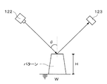
したがって、従来のようにレジスト塗布装置40内のウェハWの回転数を制御するために、塗布現像処理システム1内にテスト用ウェハを流してレジスト膜の膜厚を測定する必要がない。そのため、製品用ウェハのフォトリソグラフィー処理を行うシステムを停止させる必要をなくして、ウェハの所定の処理を円滑に行うことができ、ウェハの生産性を向上させることができる。
また、このようなウェハW上のパターンの高さHの測定は、ウェハW毎に行うことができる。これにより、レジスト塗布装置40内のウェハWの回転数の補正の精度が次第に向上し、フォトリソグラフィー処理が行われた後のウェハW上に形成されるパターンの精度が向上する。
また制御部130における制御についても、上記実施の形態においてはウェハWの回転数のみを制御するようにしていたが、これに限らずウェハWの回転時間、又は回転加速度のうち、いずれか1つを制御してもよい。またこれらの回転数、回転時間、回転加速度のうち、いずれか2つ又は3つを同時に制御するようにしてもよい。
20 パターン測定装置
40〜42 レジスト塗布装置
50〜54 現像処理装置
130 制御部
W ウェハ
Claims (7)
- 基板を回転させて、基板上に塗布液を塗布する工程を有し、基板にフォトリソグラフィー処理を行う基板の処理方法であって、
基板上に形成された前記塗布液による所定のパターンの高さを測定する工程と、
前記所定のパターンの高さに基づいて、少なくとも前記塗布液を塗布する工程における基板の回転数、回転時間、又は回転加速度のいずれかを制御する工程と、
を有することを特徴とする、基板の処理方法。 - 前記所定のパターンの高さの測定は、スキャトロメトリー法を用いることを特徴とする、請求項1に記載の基板の処理方法。
- 前記所定のパターンの高さの測定は、基板毎に行うことを特徴とする、請求項1又は2に記載の基板の処理方法。
- 請求項1〜3のいずれかに記載の基板の処理方法をコンピュータに実現させるためのプログラム。
- 基板を回転させて、基板上に塗布液を塗布する塗布装置と、基板上に形成された前記塗布液による所定のパターンを現像する現像装置と、を有する基板処理システムであって、
前記所定のパターンの高さに基づいて、少なくとも前記塗布装置内の基板の回転数、回転時間、又は回転加速度のいずれかを制御する制御部を有することを特徴とする、基板処理システム。 - 前記所定のパターンの高さはパターン測定装置によって測定され、当該パターン測定装置はスキャトロメトリー法によって測定するものであることを特徴とする、請求項5に記載の基板処理システム。
- 前記パターン測定装置は、前記基板処理システム内に設置されていることを特徴とする、請求項6に記載の基板処理システム。
Priority Applications (3)
| Application Number | Priority Date | Filing Date | Title |
|---|---|---|---|
| JP2006137578A JP4319201B2 (ja) | 2006-05-17 | 2006-05-17 | 基板の処理方法、プログラム及び基板処理システム |
| PCT/JP2007/059722 WO2007132758A1 (ja) | 2006-05-17 | 2007-05-11 | 基板の処理方法、プログラム、コンピュータ読み取り可能な記憶媒体、及び基板処理システム |
| US12/300,135 US7884950B2 (en) | 2006-05-17 | 2007-05-11 | Substrate processing method, program, computer-readable storage medium, and substrate processing system |
Applications Claiming Priority (1)
| Application Number | Priority Date | Filing Date | Title |
|---|---|---|---|
| JP2006137578A JP4319201B2 (ja) | 2006-05-17 | 2006-05-17 | 基板の処理方法、プログラム及び基板処理システム |
Publications (2)
| Publication Number | Publication Date |
|---|---|
| JP2007311469A JP2007311469A (ja) | 2007-11-29 |
| JP4319201B2 true JP4319201B2 (ja) | 2009-08-26 |
Family
ID=38693852
Family Applications (1)
| Application Number | Title | Priority Date | Filing Date |
|---|---|---|---|
| JP2006137578A Expired - Fee Related JP4319201B2 (ja) | 2006-05-17 | 2006-05-17 | 基板の処理方法、プログラム及び基板処理システム |
Country Status (3)
| Country | Link |
|---|---|
| US (1) | US7884950B2 (ja) |
| JP (1) | JP4319201B2 (ja) |
| WO (1) | WO2007132758A1 (ja) |
Families Citing this family (2)
| Publication number | Priority date | Publication date | Assignee | Title |
|---|---|---|---|---|
| JP5017147B2 (ja) | 2008-03-06 | 2012-09-05 | 東京エレクトロン株式会社 | 基板の処理方法、プログラム及びコンピュータ記憶媒体及び基板処理システム |
| JP6140990B2 (ja) | 2012-11-30 | 2017-06-07 | キヤノン株式会社 | 測定装置、インプリントシステム、測定方法及びデバイス製造方法 |
Family Cites Families (5)
| Publication number | Priority date | Publication date | Assignee | Title |
|---|---|---|---|---|
| JPS6489434A (en) * | 1987-09-30 | 1989-04-03 | Hitachi Ltd | Resist applying method |
| JPH05102031A (ja) * | 1991-10-04 | 1993-04-23 | Fujitsu Ltd | 感光性被膜の感度測定法及び耐蝕性被膜の形成法 |
| JP3589406B2 (ja) | 1999-10-25 | 2004-11-17 | 東京エレクトロン株式会社 | 基板処理システム |
| JP2005046694A (ja) * | 2003-07-31 | 2005-02-24 | Toshiba Corp | 塗布膜形成方法及び塗布装置 |
| JP2005315742A (ja) * | 2004-04-28 | 2005-11-10 | Sony Corp | 測定装置および測定方法 |
-
2006
- 2006-05-17 JP JP2006137578A patent/JP4319201B2/ja not_active Expired - Fee Related
-
2007
- 2007-05-11 WO PCT/JP2007/059722 patent/WO2007132758A1/ja not_active Ceased
- 2007-05-11 US US12/300,135 patent/US7884950B2/en not_active Expired - Fee Related
Also Published As
| Publication number | Publication date |
|---|---|
| JP2007311469A (ja) | 2007-11-29 |
| US7884950B2 (en) | 2011-02-08 |
| WO2007132758A1 (ja) | 2007-11-22 |
| US20090181316A1 (en) | 2009-07-16 |
Similar Documents
| Publication | Publication Date | Title |
|---|---|---|
| CN101527259B (zh) | 衬底的处理方法、计算机存储介质以及衬底处理系统 | |
| US11287798B2 (en) | Substrate processing capable of suppressing a decrease in throughput while reducing the impact on exposure treatment caused by warping of a substrate | |
| TWI379343B (en) | Substrate processing method and substrate processing system | |
| KR100855777B1 (ko) | 기판 처리장치와 기판 처리방법 | |
| WO2014129259A1 (ja) | 成膜方法、コンピュータ記憶媒体及び成膜システム | |
| JP2005203440A (ja) | 位置調整方法及び基板処理システム | |
| JP3178129U (ja) | 基板検査装置 | |
| JP2002260994A (ja) | 基板処理装置 | |
| JP4090986B2 (ja) | 線幅測定方法,基板の処理方法及び基板の処理装置 | |
| US8110325B2 (en) | Substrate treatment method | |
| US7525650B2 (en) | Substrate processing apparatus for performing photolithography | |
| JP6775036B2 (ja) | 成膜システム、成膜方法及びコンピュータ記憶媒体 | |
| JP2019004108A (ja) | 成膜方法、記憶媒体及び成膜システム | |
| JP3599330B2 (ja) | 基板処理方法及び基板処理装置 | |
| JP4319201B2 (ja) | 基板の処理方法、プログラム及び基板処理システム | |
| JP4970882B2 (ja) | 基板の測定方法、プログラム、プログラムを記録したコンピュータ読み取り可能な記録媒体及び基板の測定システム | |
| JP2010212414A (ja) | 基板の処理方法、プログラム、コンピュータ記憶媒体及び基板処理システム | |
| KR101387862B1 (ko) | 기판의 처리 방법, 프로그램, 컴퓨터 기억매체 및 기판 처리 시스템 | |
| JP2007110080A (ja) | 基板処理装置、基板処理方法、基板処理プログラム、及びそのプログラムを記録したコンピュータ読み取り可能な記録媒体 | |
| WO2008059686A1 (en) | Substrate processing method and substrate processing system | |
| US8105738B2 (en) | Developing method | |
| JP4920317B2 (ja) | 基板の処理方法、プログラム、コンピュータ読み取り可能な記録媒体及び基板の処理システム | |
| KR20190124679A (ko) | 기판 처리 장치 및 방법 |
Legal Events
| Date | Code | Title | Description |
|---|---|---|---|
| A621 | Written request for application examination |
Free format text: JAPANESE INTERMEDIATE CODE: A621 Effective date: 20080704 |
|
| A131 | Notification of reasons for refusal |
Free format text: JAPANESE INTERMEDIATE CODE: A131 Effective date: 20090303 |
|
| A521 | Request for written amendment filed |
Free format text: JAPANESE INTERMEDIATE CODE: A523 Effective date: 20090423 |
|
| TRDD | Decision of grant or rejection written | ||
| A01 | Written decision to grant a patent or to grant a registration (utility model) |
Free format text: JAPANESE INTERMEDIATE CODE: A01 Effective date: 20090526 |
|
| A01 | Written decision to grant a patent or to grant a registration (utility model) |
Free format text: JAPANESE INTERMEDIATE CODE: A01 |
|
| A61 | First payment of annual fees (during grant procedure) |
Free format text: JAPANESE INTERMEDIATE CODE: A61 Effective date: 20090527 |
|
| FPAY | Renewal fee payment (event date is renewal date of database) |
Free format text: PAYMENT UNTIL: 20120605 Year of fee payment: 3 |
|
| R150 | Certificate of patent or registration of utility model |
Ref document number: 4319201 Country of ref document: JP Free format text: JAPANESE INTERMEDIATE CODE: R150 Free format text: JAPANESE INTERMEDIATE CODE: R150 |
|
| FPAY | Renewal fee payment (event date is renewal date of database) |
Free format text: PAYMENT UNTIL: 20150605 Year of fee payment: 6 |
|
| R250 | Receipt of annual fees |
Free format text: JAPANESE INTERMEDIATE CODE: R250 |
|
| R250 | Receipt of annual fees |
Free format text: JAPANESE INTERMEDIATE CODE: R250 |
|
| R250 | Receipt of annual fees |
Free format text: JAPANESE INTERMEDIATE CODE: R250 |
|
| R250 | Receipt of annual fees |
Free format text: JAPANESE INTERMEDIATE CODE: R250 |
|
| R250 | Receipt of annual fees |
Free format text: JAPANESE INTERMEDIATE CODE: R250 |
|
| R250 | Receipt of annual fees |
Free format text: JAPANESE INTERMEDIATE CODE: R250 |
|
| LAPS | Cancellation because of no payment of annual fees |