JP4331993B2 - 電力用半導体装置 - Google Patents
電力用半導体装置 Download PDFInfo
- Publication number
- JP4331993B2 JP4331993B2 JP2003300178A JP2003300178A JP4331993B2 JP 4331993 B2 JP4331993 B2 JP 4331993B2 JP 2003300178 A JP2003300178 A JP 2003300178A JP 2003300178 A JP2003300178 A JP 2003300178A JP 4331993 B2 JP4331993 B2 JP 4331993B2
- Authority
- JP
- Japan
- Prior art keywords
- main
- power semiconductor
- insulating
- terminal
- semiconductor device
- Prior art date
- Legal status (The legal status is an assumption and is not a legal conclusion. Google has not performed a legal analysis and makes no representation as to the accuracy of the status listed.)
- Expired - Lifetime
Links
Images




Classifications
-
- H—ELECTRICITY
- H10—SEMICONDUCTOR DEVICES; ELECTRIC SOLID-STATE DEVICES NOT OTHERWISE PROVIDED FOR
- H10W—GENERIC PACKAGES, INTERCONNECTIONS, CONNECTORS OR OTHER CONSTRUCTIONAL DETAILS OF DEVICES COVERED BY CLASS H10
- H10W90/00—Package configurations
- H10W90/701—Package configurations characterised by the relative positions of pads or connectors relative to package parts
- H10W90/751—Package configurations characterised by the relative positions of pads or connectors relative to package parts of bond wires
- H10W90/753—Package configurations characterised by the relative positions of pads or connectors relative to package parts of bond wires between laterally-adjacent chips
Landscapes
- Structures Or Materials For Encapsulating Or Coating Semiconductor Devices Or Solid State Devices (AREA)
- Inverter Devices (AREA)
Description
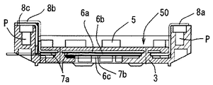
本発明の実施の形態1における端子ブロック50を適用して形成されたパワー半導体装置の内部平面図であり、この図1中のA−AラインおよびB−Bラインでの断面図を図2および図3に示す。パワー半導体装置のパッケージであるケース1の底面として熱伝導性のよい放熱板2が取付けネジにより取り付けられており、その放熱板2上でかつ、放熱板2を2分するように、樹脂ライン3が設けられる。その樹脂ライン3両側で前記放熱板2上には、それぞれ絶縁基板4が設けられ、その絶縁基板4上には所定の半導体素子5が実装されている。
2 放熱板
3 樹脂ライン
4 絶縁基板
5 半導体素子
6 主端子
7 絶縁紙
8 接続用端子
9 導電性ワイヤ
10 上蓋
21 ガイド
22 支持部材
50 端子ブロック
Q 穴
Claims (3)
- ベース板、
裏主面が前記ベース板の第1主面上に固着されると共に、表主面には回路パターンが形成された絶縁基板、
この絶縁基板の前記回路パターン上に固着された複数の電力用半導体チップ、
前記絶縁基板の一辺近傍に配設されると共に、互いの少なくとも一部同士が所定の間隔をおいて対向する複数の主端子、
前記複数の主端子を固定する樹脂ライン、
前記複数の主端子の前記間隔を置いた部分に配設され前記複数の主端子間を絶縁する絶縁層、
一端の開口端が前記ベース板の周縁部に固着し少なくとも前記絶縁基板と前記電力用半導体チップを囲繞する樹脂製のケース、
および前記電力用半導体チップと前記主端子とを接続するボンディングワイヤ
を備えた電力用半導体装置において、
前記絶縁層を前記ケースとは別体の絶縁紙とすると共に、前記主端子と前記絶縁紙の共通する箇所に穴を形成し、前記絶縁紙と前記主端子とを前記樹脂ラインに一体的に成型固定したことを特徴とする電力用半導体装置。 - ベース板、
裏主面が前記ベース板の第1主面上に固着されると共に、表主面には回路パターンが形成された第1と第2の絶縁基板、
この第1と第2の絶縁基板の夫々の前記回路パターン上に固着された複数の電力用半導体チップ、
前記第1の絶縁基板と前記第2の絶縁基板との隣接部の上部に間隔をおいて配設されると共に、互いの少なくとも一部同士が所定の間隔をおいて対向する複数の主端子、
前記複数の主端子を固定する樹脂ライン、
前記複数の主端子の前記間隔を置いた部分に配設され前記複数の主端子間を絶縁する絶縁層、
一端の開口端が前記ベース板の周縁部に固着し少なくとも前記第1と第2の絶縁基板と前記電力用半導体チップを囲繞する樹脂製のケース、
および前記電力用半導体チップと前記主端子とを接続するボンディングワイヤ
を備えた電力用半導体装置において、
前記絶縁層を前記ケースとは別体の絶縁紙とすると共に、前記主端子と前記絶縁紙の共通する箇所に穴を形成し、前記絶縁紙と前記主端子とを前記樹脂ラインに一体的に成型固定したことを特徴とする電力用半導体装置。 - 樹脂で互いに一体化された主端子と絶縁紙とからなる端子ブロックを前記ケースに着脱自在としたことを特徴とする請求項1又は2に記載の電力用半導体装置。
Priority Applications (1)
| Application Number | Priority Date | Filing Date | Title |
|---|---|---|---|
| JP2003300178A JP4331993B2 (ja) | 2002-10-11 | 2003-08-25 | 電力用半導体装置 |
Applications Claiming Priority (2)
| Application Number | Priority Date | Filing Date | Title |
|---|---|---|---|
| JP2002298633 | 2002-10-11 | ||
| JP2003300178A JP4331993B2 (ja) | 2002-10-11 | 2003-08-25 | 電力用半導体装置 |
Publications (2)
| Publication Number | Publication Date |
|---|---|
| JP2004153243A JP2004153243A (ja) | 2004-05-27 |
| JP4331993B2 true JP4331993B2 (ja) | 2009-09-16 |
Family
ID=32473592
Family Applications (1)
| Application Number | Title | Priority Date | Filing Date |
|---|---|---|---|
| JP2003300178A Expired - Lifetime JP4331993B2 (ja) | 2002-10-11 | 2003-08-25 | 電力用半導体装置 |
Country Status (1)
| Country | Link |
|---|---|
| JP (1) | JP4331993B2 (ja) |
Families Citing this family (6)
| Publication number | Priority date | Publication date | Assignee | Title |
|---|---|---|---|---|
| DE102005016650B4 (de) * | 2005-04-12 | 2009-11-19 | Semikron Elektronik Gmbh & Co. Kg | Leistungshalbleitermodul mit stumpf gelöteten Anschluss- und Verbindungselementen |
| JP5045111B2 (ja) * | 2007-01-17 | 2012-10-10 | トヨタ自動車株式会社 | 半導体モジュール及びその製造方法 |
| JPWO2012039115A1 (ja) * | 2010-09-24 | 2014-02-03 | セミコンダクター・コンポーネンツ・インダストリーズ・リミテッド・ライアビリティ・カンパニー | 回路装置 |
| JP6451747B2 (ja) | 2014-11-28 | 2019-01-16 | 富士電機株式会社 | 半導体装置 |
| CN110808190B (zh) * | 2019-11-08 | 2025-07-22 | 河南华盛隆源电气有限公司 | 真空断路器及固封极柱进出线结构 |
| JP7469969B2 (ja) * | 2020-06-26 | 2024-04-17 | 株式会社 日立パワーデバイス | パワーモジュール |
-
2003
- 2003-08-25 JP JP2003300178A patent/JP4331993B2/ja not_active Expired - Lifetime
Also Published As
| Publication number | Publication date |
|---|---|
| JP2004153243A (ja) | 2004-05-27 |
Similar Documents
| Publication | Publication Date | Title |
|---|---|---|
| EP2005470B1 (en) | Lead frame based, over-molded semiconductor package with integrated through hole technology (tht) heat spreader pin(s) and associated method of manufacturing | |
| EP1868244B1 (en) | Semiconductor device | |
| CN104037147A (zh) | 半导体装置 | |
| US6646884B1 (en) | Sandwich-structured intelligent power module | |
| JP4437860B2 (ja) | 配線ブロックの収納構造 | |
| JP2573809B2 (ja) | 電子部品内蔵のマルチチップモジュール | |
| CN115692398A (zh) | 功率模块和具有其的电子设备 | |
| US5793613A (en) | Heat-dissipating and supporting structure for a plastic package with a fully insulated heat sink for an electronic device | |
| JP6165025B2 (ja) | 半導体モジュール | |
| US6262475B1 (en) | Lead frame with heat slug | |
| JP2005191147A (ja) | 混成集積回路装置の製造方法 | |
| JP2004153243A (ja) | 電力用半導体装置 | |
| US20080036049A1 (en) | Stacked integration module and method for manufacturing the same | |
| EP4283670A2 (en) | Molded power modules | |
| JP2021125477A (ja) | 半導体装置 | |
| JP2004281804A (ja) | 回路基板 | |
| JP2795063B2 (ja) | 混成集積回路装置 | |
| KR20060105403A (ko) | 혼성회로와 복합기판을 가지는 패키지 구조물 | |
| EP0782184A1 (en) | Heat dissipating and supporting structure for a package | |
| JP2018082069A (ja) | 半導体装置および半導体装置の製造方法 | |
| JP2004134624A (ja) | 電力用半導体装置 | |
| JPH09121018A (ja) | 半導体装置 | |
| JPH04237154A (ja) | 半導体パッケージ | |
| CN117012743A (zh) | 电子器件组件 | |
| JP2939094B2 (ja) | 電力用半導体装置の製造方法 |
Legal Events
| Date | Code | Title | Description |
|---|---|---|---|
| A621 | Written request for application examination |
Free format text: JAPANESE INTERMEDIATE CODE: A621 Effective date: 20060105 |
|
| A977 | Report on retrieval |
Free format text: JAPANESE INTERMEDIATE CODE: A971007 Effective date: 20060517 |
|
| RD03 | Notification of appointment of power of attorney |
Free format text: JAPANESE INTERMEDIATE CODE: A7423 Effective date: 20080131 |
|
| A131 | Notification of reasons for refusal |
Free format text: JAPANESE INTERMEDIATE CODE: A131 Effective date: 20090224 |
|
| A521 | Request for written amendment filed |
Free format text: JAPANESE INTERMEDIATE CODE: A523 Effective date: 20090421 |
|
| TRDD | Decision of grant or rejection written | ||
| A01 | Written decision to grant a patent or to grant a registration (utility model) |
Free format text: JAPANESE INTERMEDIATE CODE: A01 Effective date: 20090526 |
|
| A01 | Written decision to grant a patent or to grant a registration (utility model) |
Free format text: JAPANESE INTERMEDIATE CODE: A01 |
|
| A61 | First payment of annual fees (during grant procedure) |
Free format text: JAPANESE INTERMEDIATE CODE: A61 Effective date: 20090619 |
|
| R150 | Certificate of patent or registration of utility model |
Ref document number: 4331993 Country of ref document: JP Free format text: JAPANESE INTERMEDIATE CODE: R150 Free format text: JAPANESE INTERMEDIATE CODE: R150 |
|
| FPAY | Renewal fee payment (event date is renewal date of database) |
Free format text: PAYMENT UNTIL: 20120626 Year of fee payment: 3 |
|
| FPAY | Renewal fee payment (event date is renewal date of database) |
Free format text: PAYMENT UNTIL: 20130626 Year of fee payment: 4 |
|
| R250 | Receipt of annual fees |
Free format text: JAPANESE INTERMEDIATE CODE: R250 |
|
| R250 | Receipt of annual fees |
Free format text: JAPANESE INTERMEDIATE CODE: R250 |
|
| R250 | Receipt of annual fees |
Free format text: JAPANESE INTERMEDIATE CODE: R250 |
|
| R250 | Receipt of annual fees |
Free format text: JAPANESE INTERMEDIATE CODE: R250 |
|
| R250 | Receipt of annual fees |
Free format text: JAPANESE INTERMEDIATE CODE: R250 |
|
| R250 | Receipt of annual fees |
Free format text: JAPANESE INTERMEDIATE CODE: R250 |
|
| R250 | Receipt of annual fees |
Free format text: JAPANESE INTERMEDIATE CODE: R250 |
|
| R250 | Receipt of annual fees |
Free format text: JAPANESE INTERMEDIATE CODE: R250 |
|
| EXPY | Cancellation because of completion of term |