JP4337467B2 - 光走査装置の検査方法 - Google Patents
光走査装置の検査方法 Download PDFInfo
- Publication number
- JP4337467B2 JP4337467B2 JP2003293049A JP2003293049A JP4337467B2 JP 4337467 B2 JP4337467 B2 JP 4337467B2 JP 2003293049 A JP2003293049 A JP 2003293049A JP 2003293049 A JP2003293049 A JP 2003293049A JP 4337467 B2 JP4337467 B2 JP 4337467B2
- Authority
- JP
- Japan
- Prior art keywords
- substrate
- detection element
- synchronization detection
- light
- optical scanning
- Prior art date
- Legal status (The legal status is an assumption and is not a legal conclusion. Google has not performed a legal analysis and makes no representation as to the accuracy of the status listed.)
- Expired - Fee Related
Links
- 230000003287 optical effect Effects 0.000 title claims description 35
- 238000007689 inspection Methods 0.000 title claims description 26
- 238000000034 method Methods 0.000 title claims description 13
- 238000001514 detection method Methods 0.000 claims description 46
- 239000000758 substrate Substances 0.000 claims description 40
- 239000004065 semiconductor Substances 0.000 claims description 12
- 230000001360 synchronised effect Effects 0.000 claims description 8
- 230000015572 biosynthetic process Effects 0.000 claims description 3
- 238000001816 cooling Methods 0.000 description 7
- 239000003990 capacitor Substances 0.000 description 6
- 125000006850 spacer group Chemical group 0.000 description 6
- XAGFODPZIPBFFR-UHFFFAOYSA-N aluminium Chemical compound [Al] XAGFODPZIPBFFR-UHFFFAOYSA-N 0.000 description 3
- 229910052782 aluminium Inorganic materials 0.000 description 3
- 239000000463 material Substances 0.000 description 3
- 239000006059 cover glass Substances 0.000 description 2
- 230000035945 sensitivity Effects 0.000 description 2
- JOYRKODLDBILNP-UHFFFAOYSA-N Ethyl urethane Chemical compound CCOC(N)=O JOYRKODLDBILNP-UHFFFAOYSA-N 0.000 description 1
- 230000003247 decreasing effect Effects 0.000 description 1
- 238000010586 diagram Methods 0.000 description 1
- 230000004907 flux Effects 0.000 description 1
- 108091008695 photoreceptors Proteins 0.000 description 1
- 229910000679 solder Inorganic materials 0.000 description 1
Images


Classifications
-
- H—ELECTRICITY
- H04—ELECTRIC COMMUNICATION TECHNIQUE
- H04N—PICTORIAL COMMUNICATION, e.g. TELEVISION
- H04N1/00—Scanning, transmission or reproduction of documents or the like, e.g. facsimile transmission; Details thereof
- H04N1/04—Scanning arrangements, i.e. arrangements for the displacement of active reading or reproducing elements relative to the original or reproducing medium, or vice versa
- H04N1/047—Detection, control or error compensation of scanning velocity or position
-
- G—PHYSICS
- G02—OPTICS
- G02B—OPTICAL ELEMENTS, SYSTEMS OR APPARATUS
- G02B26/00—Optical devices or arrangements for the control of light using movable or deformable optical elements
- G02B26/08—Optical devices or arrangements for the control of light using movable or deformable optical elements for controlling the direction of light
- G02B26/10—Scanning systems
- G02B26/12—Scanning systems using multifaceted mirrors
-
- G—PHYSICS
- G03—PHOTOGRAPHY; CINEMATOGRAPHY; ANALOGOUS TECHNIQUES USING WAVES OTHER THAN OPTICAL WAVES; ELECTROGRAPHY; HOLOGRAPHY
- G03G—ELECTROGRAPHY; ELECTROPHOTOGRAPHY; MAGNETOGRAPHY
- G03G15/00—Apparatus for electrographic processes using a charge pattern
- G03G15/04—Apparatus for electrographic processes using a charge pattern for exposing, i.e. imagewise exposure by optically projecting the original image on a photoconductive recording material
- G03G15/043—Apparatus for electrographic processes using a charge pattern for exposing, i.e. imagewise exposure by optically projecting the original image on a photoconductive recording material with means for controlling illumination or exposure
- G03G15/0435—Apparatus for electrographic processes using a charge pattern for exposing, i.e. imagewise exposure by optically projecting the original image on a photoconductive recording material with means for controlling illumination or exposure by introducing an optical element in the optical path, e.g. a filter
-
- H—ELECTRICITY
- H04—ELECTRIC COMMUNICATION TECHNIQUE
- H04N—PICTORIAL COMMUNICATION, e.g. TELEVISION
- H04N1/00—Scanning, transmission or reproduction of documents or the like, e.g. facsimile transmission; Details thereof
- H04N1/00519—Constructional details not otherwise provided for, e.g. housings, covers
- H04N1/00525—Providing a more compact apparatus, e.g. sheet discharge tray in cover
-
- H—ELECTRICITY
- H04—ELECTRIC COMMUNICATION TECHNIQUE
- H04N—PICTORIAL COMMUNICATION, e.g. TELEVISION
- H04N1/00—Scanning, transmission or reproduction of documents or the like, e.g. facsimile transmission; Details thereof
- H04N1/04—Scanning arrangements, i.e. arrangements for the displacement of active reading or reproducing elements relative to the original or reproducing medium, or vice versa
- H04N1/113—Scanning arrangements, i.e. arrangements for the displacement of active reading or reproducing elements relative to the original or reproducing medium, or vice versa using oscillating or rotating mirrors
- H04N1/1135—Scanning arrangements, i.e. arrangements for the displacement of active reading or reproducing elements relative to the original or reproducing medium, or vice versa using oscillating or rotating mirrors for the main-scan only
-
- H—ELECTRICITY
- H04—ELECTRIC COMMUNICATION TECHNIQUE
- H04N—PICTORIAL COMMUNICATION, e.g. TELEVISION
- H04N2201/00—Indexing scheme relating to scanning, transmission or reproduction of documents or the like, and to details thereof
- H04N2201/0077—Types of the still picture apparatus
- H04N2201/0082—Image hardcopy reproducer
-
- H—ELECTRICITY
- H04—ELECTRIC COMMUNICATION TECHNIQUE
- H04N—PICTORIAL COMMUNICATION, e.g. TELEVISION
- H04N2201/00—Indexing scheme relating to scanning, transmission or reproduction of documents or the like, and to details thereof
- H04N2201/04—Scanning arrangements
- H04N2201/047—Detection, control or error compensation of scanning velocity or position
- H04N2201/04701—Detection of scanning velocity or position
- H04N2201/0471—Detection of scanning velocity or position using dedicated detectors
- H04N2201/04713—Details of the detector arrangement, e.g. non-standard position, optical details
-
- H—ELECTRICITY
- H04—ELECTRIC COMMUNICATION TECHNIQUE
- H04N—PICTORIAL COMMUNICATION, e.g. TELEVISION
- H04N2201/00—Indexing scheme relating to scanning, transmission or reproduction of documents or the like, and to details thereof
- H04N2201/04—Scanning arrangements
- H04N2201/047—Detection, control or error compensation of scanning velocity or position
- H04N2201/04701—Detection of scanning velocity or position
- H04N2201/04729—Detection of scanning velocity or position in the main-scan direction
-
- H—ELECTRICITY
- H04—ELECTRIC COMMUNICATION TECHNIQUE
- H04N—PICTORIAL COMMUNICATION, e.g. TELEVISION
- H04N2201/00—Indexing scheme relating to scanning, transmission or reproduction of documents or the like, and to details thereof
- H04N2201/04—Scanning arrangements
- H04N2201/047—Detection, control or error compensation of scanning velocity or position
- H04N2201/04701—Detection of scanning velocity or position
- H04N2201/04744—Detection of scanning velocity or position by detecting the scanned beam or a reference beam
Landscapes
- Physics & Mathematics (AREA)
- General Physics & Mathematics (AREA)
- Optics & Photonics (AREA)
- Engineering & Computer Science (AREA)
- Multimedia (AREA)
- Signal Processing (AREA)
- Mechanical Optical Scanning Systems (AREA)
- Facsimile Scanning Arrangements (AREA)
- Laser Beam Printer (AREA)
Description
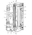
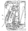
図1は、本発明に係る光走査装置の一実施形態としてのスキャナの正面部を示す。図2は、スキャナの上面カバーを示す図である。図3は、スキャナの裏面図である。図4は、スキャナの基板が取り外された状態を示す透視図である。
図1において、スキャナ60の正面部は、光源3、基板4、ポリゴンモータ12、Fシータレンズ14、折り返しミラー16および筐体22などで構成されている。
基板4は、スキャナ60の前側の左端部に配設された平板であり、その上面にはコネクタ31、回路素子32a〜32e、コンデンサ33aなどが実装され、その下面は半田で接続された電気回路面で構成されている。基板4の下面には、後述の同期検出素子48が取り付けられている。同期検出素子48が、基板4の下面に取り付けられているので基板4の上面に実装されるコネクタ31、回路素子32a〜32e、コンデンサ33aなどの配置を自由に選択することができる。基板4は、ネジ5によって筐体22に固定されている。
なお、スキャナ60の上面は、図2に示す上面カバー25によって覆われ、スキャナ60の正面側に配置された部品が保護されている。上面カバー25は、上面カバー取付けネジ26によってスポンジ30a、30b、30cなどを介して筐体22に取り付けられている。
図1に示す光源3から射出された光束は、コリメータレンズホルダ7によって支持されたコリメータレンズ8を通過する。コリメータレンズ8を通過して平行光となった光束は、コリメータスリット9を通過した後、さらにシリンドリカルレンズ11を通過する。シリンドリカルレンズ11を通過した光束は、ポリゴンモータ12に一体的に形成され高速で回転する反射体12aで偏向走査されて偏向光を生ずる。この偏向光は、Fシータレンズを通過し、スキャナ60の後側(図1のR方向側)に配設され押さえバネ34によって取り付けられている折り返しミラー16によって直角に光路が変更され、その偏向光の一部はスキャナ60の裏面に到達する。
図3に戻り、スキャナ60のポリゴンモータ12の冷却手段は裏面側の前側(図3のF方向側)の右端部に設けられている。図3のC方向から見た冷却手段を図6に概略的に示す。
以上、本発明に係る一実施形態について説明したが、本発明の実施の形態は、上記実施例に何ら限定されることなく、本発明の技術的範囲に属する限り種々の形態を取りうることはいうまでもない。
Claims (4)
- 回路素子が組み付けられた基板と、
該基板の上面に組み付けられた回路素子により出力が制御される光源と、
該光源から射出される光束を偏向走査する反射体と、
該反射体からの偏向光の一部を取り込み、像形成のための同期検出を行う同期検出素子と、
該同期検出素子へ前記反射体からの偏向光を導入するための集光レンズと、
前記基板、光源、反射体及び同期検出素子が組み付けられる筐体とを備えた光走査装置の検査方法であって、
前記基板は、前記筐体の上面又は下面と平行に組みつけられるとともに、貫通孔を有し、
前記同期検出素子は、前記基板の下面に組み付けられ、前記基板の下側に設けられた光路を通る前記偏向光を検知し、
前記偏向光を通過させるための検査孔が形成された検査板を前記貫通孔に挿通することで、前記同期検出素子と前記集光レンズの組み付けアライメントを検査する
ことを特徴とする光走査装置の検査方法。 - 前記光源は、少なくとも一つの発光素子を備えた半導体レーザであることを特徴とする、請求項1記載の光走査装置の検査方法。
- 前記検査孔の面積は、前記貫通孔に挿通された前記検査板と前記同期検出素子との間に配設された前記集光レンズの有効面積よりも小さいことを特徴とする、請求項1または請求項2に記載の光走査装置の検査方法。
- 前記基板を下側から支持する前記筐体に、前記筐体の強度および剛性を増加させるリブが形成されていることを特徴とする、請求項1ないし3のいずれかに記載の光走査装置の検査方法。
Priority Applications (5)
| Application Number | Priority Date | Filing Date | Title |
|---|---|---|---|
| JP2003293049A JP4337467B2 (ja) | 2003-08-13 | 2003-08-13 | 光走査装置の検査方法 |
| US10/914,148 US7446910B2 (en) | 2003-08-13 | 2004-08-10 | Optical scanning device |
| CNB2004100581754A CN100359412C (zh) | 2003-08-13 | 2004-08-13 | 光学扫描装置及使用它的成像装置 |
| CNU2004200877890U CN2762188Y (zh) | 2003-08-13 | 2004-08-13 | 光学扫描装置及使用它的成像装置 |
| HK05106320.3A HK1073891B (en) | 2003-08-13 | 2005-07-25 | Optical scanning device and image forming device using the same |
Applications Claiming Priority (1)
| Application Number | Priority Date | Filing Date | Title |
|---|---|---|---|
| JP2003293049A JP4337467B2 (ja) | 2003-08-13 | 2003-08-13 | 光走査装置の検査方法 |
Publications (2)
| Publication Number | Publication Date |
|---|---|
| JP2005062516A JP2005062516A (ja) | 2005-03-10 |
| JP4337467B2 true JP4337467B2 (ja) | 2009-09-30 |
Family
ID=34370170
Family Applications (1)
| Application Number | Title | Priority Date | Filing Date |
|---|---|---|---|
| JP2003293049A Expired - Fee Related JP4337467B2 (ja) | 2003-08-13 | 2003-08-13 | 光走査装置の検査方法 |
Country Status (3)
| Country | Link |
|---|---|
| US (1) | US7446910B2 (ja) |
| JP (1) | JP4337467B2 (ja) |
| CN (2) | CN100359412C (ja) |
Cited By (1)
| Publication number | Priority date | Publication date | Assignee | Title |
|---|---|---|---|---|
| KR20210057210A (ko) * | 2014-09-02 | 2021-05-20 | 카티바, 인크. | 산업용 프린팅 시스템에서 액적 파라미터의 빠른 측정 |
Families Citing this family (11)
| Publication number | Priority date | Publication date | Assignee | Title |
|---|---|---|---|---|
| JP4337467B2 (ja) * | 2003-08-13 | 2009-09-30 | ブラザー工業株式会社 | 光走査装置の検査方法 |
| JP4634819B2 (ja) * | 2005-02-22 | 2011-02-16 | 株式会社リコー | 光走査装置および画像形成装置 |
| JP4654074B2 (ja) * | 2005-06-15 | 2011-03-16 | キヤノン株式会社 | 光学ユニット及び画像形成装置 |
| JP5153222B2 (ja) * | 2007-06-18 | 2013-02-27 | キヤノン株式会社 | 画像形成装置 |
| JP5812704B2 (ja) * | 2011-06-09 | 2015-11-17 | キヤノン株式会社 | 走査光学装置及びそれを備えた画像形成装置 |
| JP2013167676A (ja) * | 2012-02-14 | 2013-08-29 | Kyocera Document Solutions Inc | 画像形成装置 |
| JP6145425B2 (ja) * | 2014-05-19 | 2017-06-14 | 京セラドキュメントソリューションズ株式会社 | 画像形成装置 |
| WO2015194283A1 (ja) * | 2014-06-20 | 2015-12-23 | 京セラドキュメントソリューションズ株式会社 | 光走査装置およびそれを備えた画像形成装置 |
| JP7052390B2 (ja) * | 2018-02-08 | 2022-04-12 | 船井電機株式会社 | 光走査装置 |
| JP2019191356A (ja) * | 2018-04-25 | 2019-10-31 | キヤノン株式会社 | 光走査装置及び画像形成装置 |
| CN112346239B (zh) * | 2019-08-07 | 2022-10-18 | 华为技术有限公司 | 激光扫描装置 |
Family Cites Families (11)
| Publication number | Priority date | Publication date | Assignee | Title |
|---|---|---|---|---|
| US4992827A (en) * | 1987-12-28 | 1991-02-12 | Canon Kabushiki Kaisha | Image forming apparatus |
| JPH07113972A (ja) | 1993-10-20 | 1995-05-02 | Seiko Epson Corp | 光走査装置 |
| US5917882A (en) * | 1996-11-29 | 1999-06-29 | Continental X-Ray Corporation | Radiographic/fluoroscopic imaging system with reduced patient dose and faster transitions between radiographic and fluoroscopic modes |
| JP4346729B2 (ja) * | 1999-04-05 | 2009-10-21 | シャープ株式会社 | 光走査装置 |
| JP4469034B2 (ja) * | 1999-07-26 | 2010-05-26 | 株式会社リコー | 光走査装置及びそれを備えた電子写真装置 |
| US20010030736A1 (en) * | 1999-12-23 | 2001-10-18 | Spence Stuart T. | Film conversion device with heating element |
| JP2001281577A (ja) * | 2000-03-29 | 2001-10-10 | Fuji Photo Film Co Ltd | 走査光学系及び画像記録装置 |
| US20020019940A1 (en) * | 2000-06-16 | 2002-02-14 | Matteson Craig S. | Method and apparatus for assigning test and assessment instruments to users |
| JP2002006395A (ja) * | 2000-06-26 | 2002-01-09 | Canon Inc | 画像表示装置 |
| JP2002287064A (ja) * | 2001-03-23 | 2002-10-03 | Sharp Corp | 光走査装置 |
| JP4337467B2 (ja) * | 2003-08-13 | 2009-09-30 | ブラザー工業株式会社 | 光走査装置の検査方法 |
-
2003
- 2003-08-13 JP JP2003293049A patent/JP4337467B2/ja not_active Expired - Fee Related
-
2004
- 2004-08-10 US US10/914,148 patent/US7446910B2/en active Active
- 2004-08-13 CN CNB2004100581754A patent/CN100359412C/zh not_active Expired - Fee Related
- 2004-08-13 CN CNU2004200877890U patent/CN2762188Y/zh not_active Expired - Lifetime
Cited By (2)
| Publication number | Priority date | Publication date | Assignee | Title |
|---|---|---|---|---|
| KR20210057210A (ko) * | 2014-09-02 | 2021-05-20 | 카티바, 인크. | 산업용 프린팅 시스템에서 액적 파라미터의 빠른 측정 |
| KR102414026B1 (ko) | 2014-09-02 | 2022-06-28 | 카티바, 인크. | 산업용 프린팅 시스템에서 액적 파라미터의 빠른 측정 |
Also Published As
| Publication number | Publication date |
|---|---|
| US20060098994A1 (en) | 2006-05-11 |
| CN2762188Y (zh) | 2006-03-01 |
| CN100359412C (zh) | 2008-01-02 |
| JP2005062516A (ja) | 2005-03-10 |
| US7446910B2 (en) | 2008-11-04 |
| CN1580964A (zh) | 2005-02-16 |
| HK1073891A1 (zh) | 2005-10-21 |
Similar Documents
| Publication | Publication Date | Title |
|---|---|---|
| JP4337467B2 (ja) | 光走査装置の検査方法 | |
| US7019878B2 (en) | Optical deflector and optical scanner having the optical deflector | |
| JP2004191712A (ja) | 光走査装置 | |
| JP4398289B2 (ja) | 光書込装置及び画像形成装置 | |
| JP4594017B2 (ja) | 走査光学装置 | |
| JP3489151B2 (ja) | 光走査装置 | |
| JP4727402B2 (ja) | 画像形成装置 | |
| US5900961A (en) | Scanning optical device | |
| JP2010117498A (ja) | 光走査装置及び画像形成装置 | |
| JP4654564B2 (ja) | レンズの保持構造 | |
| JP4385595B2 (ja) | 光走査装置 | |
| JP2000035548A (ja) | 光走査装置の固定構造 | |
| US6995888B1 (en) | Optical scanning device | |
| JP4669656B2 (ja) | 電子写真装置 | |
| JPH07113974A (ja) | 光走査装置 | |
| JP5178574B2 (ja) | 基板ユニット及びスキャナ | |
| JP3732946B2 (ja) | 光源装置 | |
| JP2001228431A (ja) | 光書込ユニット | |
| JP2000330061A (ja) | 光走査装置 | |
| JP2000275558A (ja) | 光偏向走査装置 | |
| JPH05299774A (ja) | 半導体レーザ装置 | |
| JP3187645B2 (ja) | 光走査装置 | |
| JP2000352685A (ja) | 走査光学装置 | |
| JPH0634904A (ja) | 光走査装置 | |
| JP2007227610A (ja) | 光源装置及び光学走査装置 |
Legal Events
| Date | Code | Title | Description |
|---|---|---|---|
| A621 | Written request for application examination |
Free format text: JAPANESE INTERMEDIATE CODE: A621 Effective date: 20050926 |
|
| A131 | Notification of reasons for refusal |
Free format text: JAPANESE INTERMEDIATE CODE: A131 Effective date: 20090317 |
|
| A977 | Report on retrieval |
Free format text: JAPANESE INTERMEDIATE CODE: A971007 Effective date: 20090317 |
|
| A521 | Request for written amendment filed |
Free format text: JAPANESE INTERMEDIATE CODE: A523 Effective date: 20090515 |
|
| TRDD | Decision of grant or rejection written | ||
| A01 | Written decision to grant a patent or to grant a registration (utility model) |
Free format text: JAPANESE INTERMEDIATE CODE: A01 Effective date: 20090609 |
|
| A01 | Written decision to grant a patent or to grant a registration (utility model) |
Free format text: JAPANESE INTERMEDIATE CODE: A01 |
|
| A61 | First payment of annual fees (during grant procedure) |
Free format text: JAPANESE INTERMEDIATE CODE: A61 Effective date: 20090622 |
|
| R150 | Certificate of patent or registration of utility model |
Ref document number: 4337467 Country of ref document: JP Free format text: JAPANESE INTERMEDIATE CODE: R150 Free format text: JAPANESE INTERMEDIATE CODE: R150 |
|
| FPAY | Renewal fee payment (event date is renewal date of database) |
Free format text: PAYMENT UNTIL: 20120710 Year of fee payment: 3 |
|
| FPAY | Renewal fee payment (event date is renewal date of database) |
Free format text: PAYMENT UNTIL: 20120710 Year of fee payment: 3 |
|
| FPAY | Renewal fee payment (event date is renewal date of database) |
Free format text: PAYMENT UNTIL: 20130710 Year of fee payment: 4 |
|
| LAPS | Cancellation because of no payment of annual fees |