JP4338542B2 - 受光素子 - Google Patents
受光素子 Download PDFInfo
- Publication number
- JP4338542B2 JP4338542B2 JP2004030008A JP2004030008A JP4338542B2 JP 4338542 B2 JP4338542 B2 JP 4338542B2 JP 2004030008 A JP2004030008 A JP 2004030008A JP 2004030008 A JP2004030008 A JP 2004030008A JP 4338542 B2 JP4338542 B2 JP 4338542B2
- Authority
- JP
- Japan
- Prior art keywords
- concentration
- light receiving
- electrode
- light
- low
- Prior art date
- Legal status (The legal status is an assumption and is not a legal conclusion. Google has not performed a legal analysis and makes no representation as to the accuracy of the status listed.)
- Expired - Fee Related
Links
- 239000012535 impurity Substances 0.000 claims description 57
- 239000000758 substrate Substances 0.000 claims description 28
- 239000004065 semiconductor Substances 0.000 claims description 22
- 230000035945 sensitivity Effects 0.000 description 6
- XUIMIQQOPSSXEZ-UHFFFAOYSA-N Silicon Chemical compound [Si] XUIMIQQOPSSXEZ-UHFFFAOYSA-N 0.000 description 4
- 235000005811 Viola adunca Nutrition 0.000 description 4
- 240000009038 Viola odorata Species 0.000 description 4
- 235000013487 Viola odorata Nutrition 0.000 description 4
- 235000002254 Viola papilionacea Nutrition 0.000 description 4
- 238000006243 chemical reaction Methods 0.000 description 4
- 230000031700 light absorption Effects 0.000 description 4
- 229910052698 phosphorus Inorganic materials 0.000 description 4
- 229910052710 silicon Inorganic materials 0.000 description 4
- 239000010703 silicon Substances 0.000 description 4
- 238000009792 diffusion process Methods 0.000 description 3
- 238000012544 monitoring process Methods 0.000 description 3
- ZOXJGFHDIHLPTG-UHFFFAOYSA-N Boron Chemical compound [B] ZOXJGFHDIHLPTG-UHFFFAOYSA-N 0.000 description 2
- OAICVXFJPJFONN-UHFFFAOYSA-N Phosphorus Chemical compound [P] OAICVXFJPJFONN-UHFFFAOYSA-N 0.000 description 2
- 229910052796 boron Inorganic materials 0.000 description 2
- 239000011574 phosphorus Substances 0.000 description 2
- 229910052581 Si3N4 Inorganic materials 0.000 description 1
- VYPSYNLAJGMNEJ-UHFFFAOYSA-N Silicium dioxide Chemical compound O=[Si]=O VYPSYNLAJGMNEJ-UHFFFAOYSA-N 0.000 description 1
- 238000010521 absorption reaction Methods 0.000 description 1
- 239000000969 carrier Substances 0.000 description 1
- 230000005611 electricity Effects 0.000 description 1
- 239000011159 matrix material Substances 0.000 description 1
- 229910021421 monocrystalline silicon Inorganic materials 0.000 description 1
- HQVNEWCFYHHQES-UHFFFAOYSA-N silicon nitride Chemical compound N12[Si]34N5[Si]62N3[Si]51N64 HQVNEWCFYHHQES-UHFFFAOYSA-N 0.000 description 1
- 229910052814 silicon oxide Inorganic materials 0.000 description 1
Images




Landscapes
- Light Receiving Elements (AREA)
Description
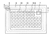
低濃度層露出領域10は、受光領域4の前面に高濃度不純物層を形成後に、この層を選択的に除去して基板表面に凹凸を形成することによって形成することも可能である。上記実施形態はシリコン半導体を用いる場合を例示したが、それ以外の半導体を用いて受光素子を形成する場合にも本発明を適用することができる。また、上記の不純物のP、Nの極性を反対の極性に変更することもできる。
2 半導体基板
3 一導電型高濃度不純物層
4 受光領域
5 絶縁膜
6 コンタクトホール
7 電極
8 逆導電型高濃度不純物層
9 電極
10 低濃度層露出領域
Claims (1)
- 低不純物濃度の半導体基板に高濃度の一導電型不純物層と逆導電型不純物層を形成し、電極に接続した一導電型の高濃度不純物層を基板表面に配置して一定面積の受光領域を形成したPN型あるいはPIN型の受光素子において、前記受光領域の中に前記半導体基板の低濃度不純物層が基板表面に露出する低濃度層露出領域を複数形成し、これらの低濃度層露出領域を前記受光領域に分散して配置するとともに、前記電極に接続した高濃度不純物層を前記電極を中心として前記受光領域の全体に亘って放射状に延びるように配置し、前記電極を前記受光領域の中央に配置し、この電極を囲むように前記低濃度層露出領域を分散して配置したことを特徴とする受光素子。
Priority Applications (1)
| Application Number | Priority Date | Filing Date | Title |
|---|---|---|---|
| JP2004030008A JP4338542B2 (ja) | 2004-02-06 | 2004-02-06 | 受光素子 |
Applications Claiming Priority (1)
| Application Number | Priority Date | Filing Date | Title |
|---|---|---|---|
| JP2004030008A JP4338542B2 (ja) | 2004-02-06 | 2004-02-06 | 受光素子 |
Publications (2)
| Publication Number | Publication Date |
|---|---|
| JP2005223160A JP2005223160A (ja) | 2005-08-18 |
| JP4338542B2 true JP4338542B2 (ja) | 2009-10-07 |
Family
ID=34998544
Family Applications (1)
| Application Number | Title | Priority Date | Filing Date |
|---|---|---|---|
| JP2004030008A Expired - Fee Related JP4338542B2 (ja) | 2004-02-06 | 2004-02-06 | 受光素子 |
Country Status (1)
| Country | Link |
|---|---|
| JP (1) | JP4338542B2 (ja) |
-
2004
- 2004-02-06 JP JP2004030008A patent/JP4338542B2/ja not_active Expired - Fee Related
Also Published As
| Publication number | Publication date |
|---|---|
| JP2005223160A (ja) | 2005-08-18 |
Similar Documents
| Publication | Publication Date | Title |
|---|---|---|
| US12113078B2 (en) | Photodetector | |
| US8994135B2 (en) | Photodiode and photodiode array | |
| US9419159B2 (en) | Semiconductor light-detecting element | |
| EP1835539A3 (en) | Photodiode array, method of manufacturing the same, and radiation detector | |
| JP5496473B2 (ja) | 裏面電極型太陽電池、太陽電池ストリングおよび太陽電池モジュール | |
| WO2010140621A1 (ja) | 半導体光検出素子及び半導体光検出素子の製造方法 | |
| JP2005259829A (ja) | 裏面入射型受光素子アレイ | |
| US8212327B2 (en) | High fill-factor laser-treated semiconductor device on bulk material with single side contact scheme | |
| JPH0799782B2 (ja) | 半導体光検出装置 | |
| JP2002083995A (ja) | 多波長フォトダイオード | |
| KR20130024740A (ko) | 고체 촬상 장치 | |
| JP2006060103A (ja) | 半導体受光装置および紫外線センサー機器 | |
| JP2005223160A (ja) | 受光素子 | |
| JPWO2011087068A1 (ja) | アバランシェフォトダイオード及びその製造方法 | |
| JP2002319669A (ja) | 裏面入射型ホトダイオード及びホトダイオードアレイ | |
| TWI660491B (zh) | 影像感測器 | |
| JP5639657B2 (ja) | 太陽電池セル | |
| CN114520268B (zh) | 光电二极管单元及光电二极管阵列 | |
| US20120305057A1 (en) | Solar battery string, solar battery module, and solar battery cell | |
| JP2006032385A (ja) | 固体撮像装置 | |
| JPH01216581A (ja) | 半導体装置 | |
| JPS6233482A (ja) | アバランシエホトダイオ−ド | |
| JPH04241458A (ja) | 半導体光検出装置 | |
| WO2022201798A1 (ja) | 受光素子アレイおよびその製造方法 | |
| JPS63204645A (ja) | 受光素子およびこの受光素子を内蔵した光電子装置 |
Legal Events
| Date | Code | Title | Description |
|---|---|---|---|
| RD01 | Notification of change of attorney |
Free format text: JAPANESE INTERMEDIATE CODE: A7421 Effective date: 20051227 |
|
| A621 | Written request for application examination |
Free format text: JAPANESE INTERMEDIATE CODE: A621 Effective date: 20060830 |
|
| A977 | Report on retrieval |
Free format text: JAPANESE INTERMEDIATE CODE: A971007 Effective date: 20081014 |
|
| A131 | Notification of reasons for refusal |
Free format text: JAPANESE INTERMEDIATE CODE: A131 Effective date: 20081021 |
|
| A521 | Request for written amendment filed |
Free format text: JAPANESE INTERMEDIATE CODE: A523 Effective date: 20081216 |
|
| A131 | Notification of reasons for refusal |
Free format text: JAPANESE INTERMEDIATE CODE: A131 Effective date: 20090217 |
|
| A521 | Request for written amendment filed |
Free format text: JAPANESE INTERMEDIATE CODE: A523 Effective date: 20090403 |
|
| TRDD | Decision of grant or rejection written | ||
| A01 | Written decision to grant a patent or to grant a registration (utility model) |
Free format text: JAPANESE INTERMEDIATE CODE: A01 Effective date: 20090602 |
|
| A01 | Written decision to grant a patent or to grant a registration (utility model) |
Free format text: JAPANESE INTERMEDIATE CODE: A01 |
|
| A61 | First payment of annual fees (during grant procedure) |
Free format text: JAPANESE INTERMEDIATE CODE: A61 Effective date: 20090630 |
|
| FPAY | Renewal fee payment (event date is renewal date of database) |
Free format text: PAYMENT UNTIL: 20120710 Year of fee payment: 3 |
|
| LAPS | Cancellation because of no payment of annual fees |