JP4376231B2 - 誘電体共振器装荷型発振回路及びこれを用いたレーダー装置 - Google Patents
誘電体共振器装荷型発振回路及びこれを用いたレーダー装置 Download PDFInfo
- Publication number
- JP4376231B2 JP4376231B2 JP2006006716A JP2006006716A JP4376231B2 JP 4376231 B2 JP4376231 B2 JP 4376231B2 JP 2006006716 A JP2006006716 A JP 2006006716A JP 2006006716 A JP2006006716 A JP 2006006716A JP 4376231 B2 JP4376231 B2 JP 4376231B2
- Authority
- JP
- Japan
- Prior art keywords
- dielectric resonator
- oscillation circuit
- voltage
- switch
- power supply
- Prior art date
- Legal status (The legal status is an assumption and is not a legal conclusion. Google has not performed a legal analysis and makes no representation as to the accuracy of the status listed.)
- Expired - Fee Related
Links
- 230000010355 oscillation Effects 0.000 title claims description 108
- 239000003990 capacitor Substances 0.000 claims description 25
- 238000010586 diagram Methods 0.000 description 15
- 238000000034 method Methods 0.000 description 11
- 230000005540 biological transmission Effects 0.000 description 9
- 239000011324 bead Substances 0.000 description 7
- 230000000694 effects Effects 0.000 description 4
- 230000002265 prevention Effects 0.000 description 3
- 238000004904 shortening Methods 0.000 description 2
- 238000007599 discharging Methods 0.000 description 1
- 238000005259 measurement Methods 0.000 description 1
- 238000012986 modification Methods 0.000 description 1
- 230000004048 modification Effects 0.000 description 1
Images


Classifications
-
- H—ELECTRICITY
- H03—ELECTRONIC CIRCUITRY
- H03B—GENERATION OF OSCILLATIONS, DIRECTLY OR BY FREQUENCY-CHANGING, BY CIRCUITS EMPLOYING ACTIVE ELEMENTS WHICH OPERATE IN A NON-SWITCHING MANNER; GENERATION OF NOISE BY SUCH CIRCUITS
- H03B5/00—Generation of oscillations using amplifier with regenerative feedback from output to input
- H03B5/18—Generation of oscillations using amplifier with regenerative feedback from output to input with frequency-determining element comprising distributed inductance and capacitance
- H03B5/1864—Generation of oscillations using amplifier with regenerative feedback from output to input with frequency-determining element comprising distributed inductance and capacitance the frequency-determining element being a dielectric resonator
- H03B5/187—Generation of oscillations using amplifier with regenerative feedback from output to input with frequency-determining element comprising distributed inductance and capacitance the frequency-determining element being a dielectric resonator the active element in the amplifier being a semiconductor device
- H03B5/1876—Generation of oscillations using amplifier with regenerative feedback from output to input with frequency-determining element comprising distributed inductance and capacitance the frequency-determining element being a dielectric resonator the active element in the amplifier being a semiconductor device the semiconductor device being a field-effect device
Landscapes
- Inductance-Capacitance Distribution Constants And Capacitance-Resistance Oscillators (AREA)
- Radar Systems Or Details Thereof (AREA)
Description
VOFF=Vgs×R61/(R61+R62+R63)
となる。一方、スイッチ73がオン状態である場合には、追加された抵抗63は短絡されることから、トランジスタ21のゲート21Gに与えられる電圧VONは、
VON=Vgs×R61/(R61+R62)
に変化する。
VOFF=Vgs×R61/(R61+R62)
となり、スイッチ74がオン状態である場合、トランジスタ21のゲート21Gに与えられる電圧VONは、
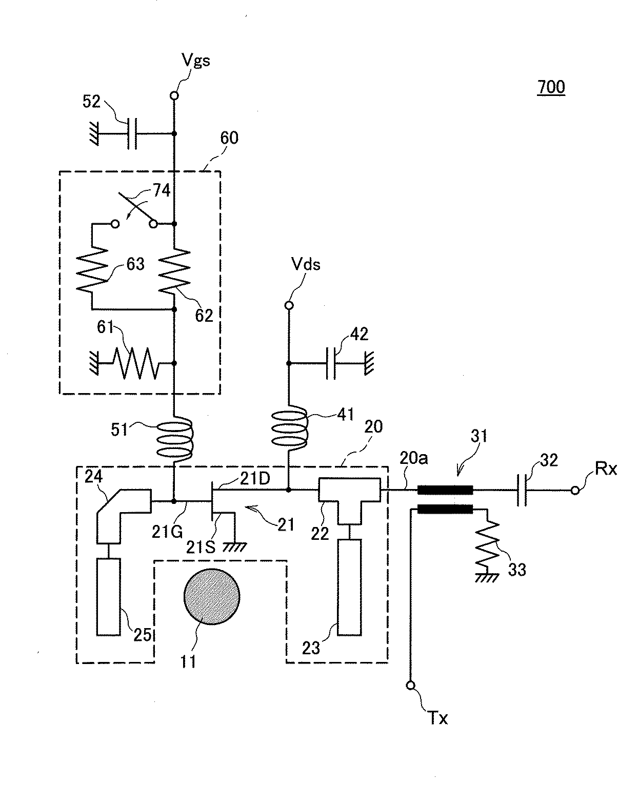
となる。
11 誘電体共振器
20 駆動回路
20a 駆動回路の出力端
21 トランジスタ
21G ゲート(制御電極)
21S ソース
21D ドレイン(被制御電極)
22〜25 信号線路
31 カプラ
32 コンデンサ
33 終端抵抗
41,51 チップビーズ
42,52,81,83 コンデンサ
60 分圧回路
61〜63,82 抵抗
71〜74 スイッチ
Rx 受信側ポート
Tx 送信側ポート
Claims (3)
- 誘電体共振器と、前記誘電体共振器に共振電圧を与える駆動回路とを備える誘電体共振器装荷型発振回路であって、
前記駆動回路は、制御電極と第1及び第2の被制御電極とを有するトランジスタと、該第1の被制御電極に接続された第1の信号線路と、該制御電極に接続された第2の信号線路とを含み、
前記誘電体共振器は前記第1の信号線路と前記第2の信号線路との間に配置され、
前記第1の被制御電極の出力は、前記第1の信号線路、前記誘電体共振器、及び前記第2の信号線路を介して前記制御電極に帰還し、
前記第1の被制御電極は、前記駆動回路が前記共振電圧を生成するために必要な第1の電圧が供給される第1の電源端子及び前記駆動回路に前記共振電圧の生成を停止させるグランド電位が供給される第2の電源端子に接続され、
前記制御電極は第3の電圧が供給される第3の電源端子に接続され、
前記第2の被制御電極はグランド電位に接続され、
前記誘電体共振器装荷型発振回路は、
前記第1の被制御電極と前記第1の電源端子との間に設けられた第1のスイッチと、
前記第1の被制御電極と前記第2の電源端子との間に設けられた第2のスイッチと、
をさらに備え、
前記第1及び第2のスイッチは排他的に導通することを特徴とする誘電体共振器装荷型発振回路。 - 前記第1のスイッチから見て前記第1の電源端子側に接続され、前記駆動回路が発生するノイズを除去するためのコンデンサをさらに備えることを特徴とする請求項1に記載の誘電体共振器装荷型発振回路。
- 請求項1又は2に記載の誘電体共振器装荷型発振回路を用いてキャリア信号を生成し、パルス変調波を生成して出力することを特徴とするレーダー装置。
Priority Applications (2)
| Application Number | Priority Date | Filing Date | Title |
|---|---|---|---|
| JP2006006716A JP4376231B2 (ja) | 2005-03-08 | 2006-01-13 | 誘電体共振器装荷型発振回路及びこれを用いたレーダー装置 |
| US11/366,304 US7378915B2 (en) | 2005-03-08 | 2006-03-01 | Dielectric resonator oscillator and radar apparatus using the same |
Applications Claiming Priority (2)
| Application Number | Priority Date | Filing Date | Title |
|---|---|---|---|
| JP2005063285 | 2005-03-08 | ||
| JP2006006716A JP4376231B2 (ja) | 2005-03-08 | 2006-01-13 | 誘電体共振器装荷型発振回路及びこれを用いたレーダー装置 |
Publications (2)
| Publication Number | Publication Date |
|---|---|
| JP2006287908A JP2006287908A (ja) | 2006-10-19 |
| JP4376231B2 true JP4376231B2 (ja) | 2009-12-02 |
Family
ID=36970192
Family Applications (1)
| Application Number | Title | Priority Date | Filing Date |
|---|---|---|---|
| JP2006006716A Expired - Fee Related JP4376231B2 (ja) | 2005-03-08 | 2006-01-13 | 誘電体共振器装荷型発振回路及びこれを用いたレーダー装置 |
Country Status (2)
| Country | Link |
|---|---|
| US (1) | US7378915B2 (ja) |
| JP (1) | JP4376231B2 (ja) |
Families Citing this family (4)
| Publication number | Priority date | Publication date | Assignee | Title |
|---|---|---|---|---|
| ATE553531T1 (de) * | 2006-10-17 | 2012-04-15 | Mitsubishi Electric Corp | Oszillator, sende-/empfangseinrichtung und frequenzsynthesizer |
| CN101930269A (zh) * | 2009-06-18 | 2010-12-29 | 鸿富锦精密工业(深圳)有限公司 | Sata控制芯片供电电路 |
| TWI429195B (zh) * | 2010-12-08 | 2014-03-01 | Ind Tech Res Inst | 功率電路及其直流對直流轉換器 |
| JP2014212469A (ja) * | 2013-04-19 | 2014-11-13 | 東京計器株式会社 | マイクロ波電力発振器及びその出力制御方法 |
Family Cites Families (5)
| Publication number | Priority date | Publication date | Assignee | Title |
|---|---|---|---|---|
| JP2947326B2 (ja) | 1994-05-23 | 1999-09-13 | 三菱電機株式会社 | 干渉防止装置 |
| GB9510028D0 (en) * | 1995-05-18 | 1995-07-12 | Cambridge Ind Ltd | Local oscillator noise rejection circuit |
| JP3661573B2 (ja) * | 2000-07-24 | 2005-06-15 | 株式会社村田製作所 | 電圧制御発振器、電圧制御発振器装置およびレーダ装置 |
| JP3914401B2 (ja) * | 2001-09-06 | 2007-05-16 | 株式会社日立製作所 | 発振器、送受信モジュール、及びレーダ装置 |
| US6714089B2 (en) * | 2002-05-29 | 2004-03-30 | Xytrans, Inc. | High frequency signal source and method of generating same using dielectric resonator oscillator (DRO) circuit |
-
2006
- 2006-01-13 JP JP2006006716A patent/JP4376231B2/ja not_active Expired - Fee Related
- 2006-03-01 US US11/366,304 patent/US7378915B2/en not_active Expired - Fee Related
Also Published As
| Publication number | Publication date |
|---|---|
| JP2006287908A (ja) | 2006-10-19 |
| US20060202770A1 (en) | 2006-09-14 |
| US7378915B2 (en) | 2008-05-27 |
Similar Documents
| Publication | Publication Date | Title |
|---|---|---|
| US7521986B2 (en) | Switch element driver circuit and semiconductor device | |
| US9862239B2 (en) | Antenna driving device | |
| US20100207747A1 (en) | Sound production controller | |
| US20100253240A1 (en) | Pwm control method and device and light adjusting device | |
| JPH09312488A (ja) | 車載用コントロールユニットのemi用接地構造 | |
| JP5806076B2 (ja) | Rfパルス信号生成用スイッチング回路、rfパルス信号生成回路、および物標探知装置 | |
| JP2005127821A (ja) | 絶縁抵抗低下検出器およびその自己診断方法 | |
| US7158074B2 (en) | Radar system and car radar system | |
| JP4376231B2 (ja) | 誘電体共振器装荷型発振回路及びこれを用いたレーダー装置 | |
| US8269476B2 (en) | Load controller to pulse width modulation-control a load | |
| EP2073386B1 (en) | Semiconductor output circuit | |
| JP2006310287A (ja) | 腐蝕防止方法、腐蝕防止装置、信号処理装置および制御ユニット | |
| US20150331089A1 (en) | Fmcw radar apparatus | |
| JP6262479B2 (ja) | アンテナ駆動装置 | |
| CN214474502U (zh) | 驱动负载的电路以及包含其的电子控制单元 | |
| JP2001168695A (ja) | 電子システム用電子ドライバ回路およびその方法 | |
| JP4390325B2 (ja) | レーダ装置及び送受信切り換え方法 | |
| JP2000346927A (ja) | レーダ用電源装置 | |
| JP5121380B2 (ja) | パルス変調器 | |
| US6133653A (en) | Recirculating driver control circuit and method of operating the same | |
| CN115943548A (zh) | 开关电源装置、开关控制装置、车载设备和车辆 | |
| US11688937B2 (en) | Antenna device | |
| JP6211360B2 (ja) | アンテナ駆動装置 | |
| US7768323B2 (en) | Device for controlling a high-voltage transistor, in particular a MOS transistor of a high-voltage radio-frequency generator for the spark ignition of an internal combustion engine | |
| JP2026052490A (ja) | 車両の電源システム |
Legal Events
| Date | Code | Title | Description |
|---|---|---|---|
| A977 | Report on retrieval |
Free format text: JAPANESE INTERMEDIATE CODE: A971007 Effective date: 20080627 |
|
| A131 | Notification of reasons for refusal |
Free format text: JAPANESE INTERMEDIATE CODE: A131 Effective date: 20080715 |
|
| A521 | Written amendment |
Free format text: JAPANESE INTERMEDIATE CODE: A523 Effective date: 20080911 |
|
| A131 | Notification of reasons for refusal |
Free format text: JAPANESE INTERMEDIATE CODE: A131 Effective date: 20090609 |
|
| A521 | Written amendment |
Free format text: JAPANESE INTERMEDIATE CODE: A523 Effective date: 20090730 |
|
| TRDD | Decision of grant or rejection written | ||
| A01 | Written decision to grant a patent or to grant a registration (utility model) |
Free format text: JAPANESE INTERMEDIATE CODE: A01 Effective date: 20090908 |
|
| A01 | Written decision to grant a patent or to grant a registration (utility model) |
Free format text: JAPANESE INTERMEDIATE CODE: A01 |
|
| A61 | First payment of annual fees (during grant procedure) |
Free format text: JAPANESE INTERMEDIATE CODE: A61 Effective date: 20090908 |
|
| R150 | Certificate of patent or registration of utility model |
Free format text: JAPANESE INTERMEDIATE CODE: R150 |
|
| FPAY | Renewal fee payment (event date is renewal date of database) |
Free format text: PAYMENT UNTIL: 20120918 Year of fee payment: 3 |
|
| FPAY | Renewal fee payment (event date is renewal date of database) |
Free format text: PAYMENT UNTIL: 20130918 Year of fee payment: 4 |
|
| LAPS | Cancellation because of no payment of annual fees |