JP4431461B2 - 表示装置の製造方法 - Google Patents
表示装置の製造方法 Download PDFInfo
- Publication number
- JP4431461B2 JP4431461B2 JP2004232781A JP2004232781A JP4431461B2 JP 4431461 B2 JP4431461 B2 JP 4431461B2 JP 2004232781 A JP2004232781 A JP 2004232781A JP 2004232781 A JP2004232781 A JP 2004232781A JP 4431461 B2 JP4431461 B2 JP 4431461B2
- Authority
- JP
- Japan
- Prior art keywords
- substrate
- solvent
- coating
- organic
- spray
- Prior art date
- Legal status (The legal status is an assumption and is not a legal conclusion. Google has not performed a legal analysis and makes no representation as to the accuracy of the status listed.)
- Expired - Fee Related
Links
Images





Classifications
-
- H—ELECTRICITY
- H10—SEMICONDUCTOR DEVICES; ELECTRIC SOLID-STATE DEVICES NOT OTHERWISE PROVIDED FOR
- H10K—ORGANIC ELECTRIC SOLID-STATE DEVICES
- H10K71/00—Manufacture or treatment specially adapted for the organic devices covered by this subclass
- H10K71/10—Deposition of organic active material
- H10K71/12—Deposition of organic active material using liquid deposition, e.g. spin coating
- H10K71/15—Deposition of organic active material using liquid deposition, e.g. spin coating characterised by the solvent used
-
- H—ELECTRICITY
- H05—ELECTRIC TECHNIQUES NOT OTHERWISE PROVIDED FOR
- H05B—ELECTRIC HEATING; ELECTRIC LIGHT SOURCES NOT OTHERWISE PROVIDED FOR; CIRCUIT ARRANGEMENTS FOR ELECTRIC LIGHT SOURCES, IN GENERAL
- H05B33/00—Electroluminescent light sources
- H05B33/10—Apparatus or processes specially adapted to the manufacture of electroluminescent light sources
-
- H—ELECTRICITY
- H10—SEMICONDUCTOR DEVICES; ELECTRIC SOLID-STATE DEVICES NOT OTHERWISE PROVIDED FOR
- H10K—ORGANIC ELECTRIC SOLID-STATE DEVICES
- H10K50/00—Organic light-emitting devices
- H10K50/10—OLEDs or polymer light-emitting diodes [PLED]
- H10K50/17—Carrier injection layers
-
- H—ELECTRICITY
- H10—SEMICONDUCTOR DEVICES; ELECTRIC SOLID-STATE DEVICES NOT OTHERWISE PROVIDED FOR
- H10K—ORGANIC ELECTRIC SOLID-STATE DEVICES
- H10K59/00—Integrated devices, or assemblies of multiple devices, comprising at least one organic light-emitting element covered by group H10K50/00
- H10K59/10—OLED displays
- H10K59/17—Passive-matrix OLED displays
-
- H—ELECTRICITY
- H10—SEMICONDUCTOR DEVICES; ELECTRIC SOLID-STATE DEVICES NOT OTHERWISE PROVIDED FOR
- H10K—ORGANIC ELECTRIC SOLID-STATE DEVICES
- H10K71/00—Manufacture or treatment specially adapted for the organic devices covered by this subclass
Landscapes
- Engineering & Computer Science (AREA)
- Manufacturing & Machinery (AREA)
- Electroluminescent Light Sources (AREA)
- Application Of Or Painting With Fluid Materials (AREA)
- Devices For Indicating Variable Information By Combining Individual Elements (AREA)
Description
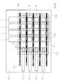
5 陰極配線
10 隔壁
11 基板
21 陰極接続配線
22 絶縁膜
23 開口部
24 表示領域
25 コンタクトホール
31 開口部
40 有機発光層
41 ポリマーバッファ層
42 ホール注入層
43 ホール輸送層
44 発光層
45 電子輸送層
46 電子注入層
50 スプレー塗布装置
51 ステージ
52 基板
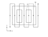
53 マスク
54 スプレーノズル
55 溶液
56 フィルタ
57 コントローラ
62 捕水材
63 対向基板
64 シール材
65 光学シート
66 捕水材収納部
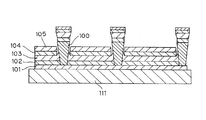
100 隔壁
101 陽極配線
102 ホール注入輸送層
103 発光層
104 電子注入輸送層
105 陰極配線
110 表示基板
111 基板
121 陰極接続配線
123 開口部
124 有機薄膜層
Claims (5)
- 表示装置用の有機膜の少なくとも一部となる溶質が溶解された塗布溶液をスプレー塗布により形成する表示装置の製造方法であって、
前記塗布溶液を基板にスプレー塗布するスプレー塗布工程と、
前記基板を乾燥させ、前記スプレー塗布された塗布溶液に含まれる溶媒を蒸発させる乾燥工程とを備え、
前記塗布溶液が、
前記溶質を1質量%以上溶解させることができる第1の溶媒と、
前記基板に塗布溶液が着滴するまでの間にすべてが揮発する揮発性溶媒とを備える表示装置の製造方法。 - 前記揮発性溶媒は、沸点が120℃以下又は、25℃における蒸気圧が400Pa以上である請求項1に記載の表示装置の製造方法。
- 前記スプレー塗布工程では、前記第1の溶媒及び前記揮発性溶媒より粘度の高い第2の溶媒をさらに備えた塗布溶液をスプレー塗布する請求項1又は2に記載の表示装置の製造方法。
- 前記スプレー塗布工程の前に、
前記揮発性溶媒のみを確認用基板に噴出して、前記確認用基板に前記揮発性溶媒が付着しないことを確認する確認工程を備え、
前記確認工程と同じ条件で、前記塗布溶液をスプレー塗布する請求項1、2又は3に記載の表示装置の製造方法。 - 前記スプレー塗布工程の前に、
前記塗布溶液をスプレー塗布するスプレーノズルと前記確認用基板との間の間隔を変えて、前記揮発性溶媒のみを噴出させる噴出工程と、
前記基板に噴出された前記揮発性溶媒が当該基板に着滴しているか否かを確認する工程をさらに備え、
前記スプレー塗布工程では、前記確認用基板に前記揮発性溶媒が着滴しないことが確認された前記スプレーノズルと前記基板との間の間隔以上の間隔で、前記塗布溶液を前記基板にスプレー塗布する請求項1、2又は3記載の表示装置の製造方法。
Priority Applications (5)
| Application Number | Priority Date | Filing Date | Title |
|---|---|---|---|
| JP2004232781A JP4431461B2 (ja) | 2004-08-09 | 2004-08-09 | 表示装置の製造方法 |
| US11/198,147 US20060033080A1 (en) | 2004-08-09 | 2005-08-08 | Mixed solution for a display device and method for fabricating a display device by using the same |
| TW094126741A TW200610433A (en) | 2004-08-09 | 2005-08-08 | Mixed solution for display device and manufacturing method of the display device using the same |
| CNB2005100919271A CN100479629C (zh) | 2004-08-09 | 2005-08-09 | 显示装置用的混合溶液及使用其的显示装置的制造方法 |
| KR1020050072816A KR20060050335A (ko) | 2004-08-09 | 2005-08-09 | 표시 장치용 혼합 용액 및 그것을 사용한 표시 장치의 제조방법 |
Applications Claiming Priority (1)
| Application Number | Priority Date | Filing Date | Title |
|---|---|---|---|
| JP2004232781A JP4431461B2 (ja) | 2004-08-09 | 2004-08-09 | 表示装置の製造方法 |
Publications (2)
| Publication Number | Publication Date |
|---|---|
| JP2006054063A JP2006054063A (ja) | 2006-02-23 |
| JP4431461B2 true JP4431461B2 (ja) | 2010-03-17 |
Family
ID=35799152
Family Applications (1)
| Application Number | Title | Priority Date | Filing Date |
|---|---|---|---|
| JP2004232781A Expired - Fee Related JP4431461B2 (ja) | 2004-08-09 | 2004-08-09 | 表示装置の製造方法 |
Country Status (5)
| Country | Link |
|---|---|
| US (1) | US20060033080A1 (ja) |
| JP (1) | JP4431461B2 (ja) |
| KR (1) | KR20060050335A (ja) |
| CN (1) | CN100479629C (ja) |
| TW (1) | TW200610433A (ja) |
Families Citing this family (9)
| Publication number | Priority date | Publication date | Assignee | Title |
|---|---|---|---|---|
| EP1842223A1 (en) * | 2004-12-27 | 2007-10-10 | OTB Group B.V. | Method for manufacturing an oled or a blank for forming an oled as well as such a blank or oled |
| US10651063B2 (en) * | 2005-06-18 | 2020-05-12 | Frederick A. Flitsch | Methods of prototyping and manufacturing with cleanspace fabricators |
| KR101097927B1 (ko) * | 2005-08-18 | 2011-12-23 | 재단법인서울대학교산학협력재단 | 액정 표시장치 제조 방법 |
| KR101413129B1 (ko) * | 2005-10-28 | 2014-07-01 | 닛산 가가쿠 고교 가부시키 가이샤 | 스프레이 또는 잉크젯 도포용 전하 수송성 바니시 |
| KR101227138B1 (ko) * | 2006-03-29 | 2013-01-28 | 엘지디스플레이 주식회사 | 폴리이미드막 도포 장치 및 그 방법 |
| KR101570891B1 (ko) * | 2008-03-06 | 2015-11-20 | 메르크 파텐트 게엠베하 | 유기 반도체 조성물 |
| JP5663395B2 (ja) * | 2011-05-10 | 2015-02-04 | 旭サナック株式会社 | 高分子超薄膜の製造方法及び高分子超薄膜の製造装置 |
| JP2018132893A (ja) * | 2017-02-14 | 2018-08-23 | 株式会社ユー・コーポレーション | タッチ式操作パネル |
| CN106803537A (zh) * | 2017-02-20 | 2017-06-06 | 安徽师范大学 | 一种构建局部清洁环境保护薄膜生长的装置 |
Family Cites Families (8)
| Publication number | Priority date | Publication date | Assignee | Title |
|---|---|---|---|---|
| JP3075290B2 (ja) * | 1991-02-28 | 2000-08-14 | 三菱瓦斯化学株式会社 | 半導体基板の洗浄液 |
| DE69428391T2 (de) * | 1993-03-25 | 2002-07-04 | Tokyo Electron Ltd., Tokio/Tokyo | Verfahren und Vorrichtung zur Beschichtung eines Filmes |
| CN1157504C (zh) * | 2000-03-21 | 2004-07-14 | 亚洲电镀器材有限公司 | 混合设备 |
| JP4762411B2 (ja) * | 2000-06-26 | 2011-08-31 | パナソニック株式会社 | 二次電池用非水電解液およびこれを用いた非水電解液二次電池 |
| DE10049201A1 (de) * | 2000-10-05 | 2002-04-11 | Clariant Gmbh | Verfahren zur Feinverteilung von organischen Pigmenten durch Fällung |
| KR100566840B1 (ko) * | 2002-01-30 | 2006-04-03 | 가부시끼가이샤 도시바 | 성막 방법 및 성막 장치 |
| AU2003277541A1 (en) * | 2002-11-11 | 2004-06-03 | Semiconductor Energy Laboratory Co., Ltd. | Process for fabricating light emitting device |
| US20050067949A1 (en) * | 2003-09-30 | 2005-03-31 | Sriram Natarajan | Solvent mixtures for an organic electronic device |
-
2004
- 2004-08-09 JP JP2004232781A patent/JP4431461B2/ja not_active Expired - Fee Related
-
2005
- 2005-08-08 TW TW094126741A patent/TW200610433A/zh not_active IP Right Cessation
- 2005-08-08 US US11/198,147 patent/US20060033080A1/en not_active Abandoned
- 2005-08-09 CN CNB2005100919271A patent/CN100479629C/zh not_active Expired - Fee Related
- 2005-08-09 KR KR1020050072816A patent/KR20060050335A/ko not_active Withdrawn
Also Published As
| Publication number | Publication date |
|---|---|
| TW200610433A (en) | 2006-03-16 |
| JP2006054063A (ja) | 2006-02-23 |
| TWI298001B (ja) | 2008-06-11 |
| KR20060050335A (ko) | 2006-05-19 |
| US20060033080A1 (en) | 2006-02-16 |
| CN1735300A (zh) | 2006-02-15 |
| CN100479629C (zh) | 2009-04-15 |
Similar Documents
| Publication | Publication Date | Title |
|---|---|---|
| US10580841B2 (en) | High resolution organic light-emitting diode devices, displays, and related method | |
| KR102095174B1 (ko) | 고해상도 유기 발광 다이오드 장치 | |
| JP4255724B2 (ja) | 有機elディスプレイの製造方法および有機elディスプレイ | |
| US20210167147A1 (en) | Light emitting device, display panel having the same, and method of manufacturing display panel | |
| CN1992157B (zh) | 显示装置的制造装置及显示装置的制造方法 | |
| KR20140074629A (ko) | 잉크젯 프린트 헤드, 이를 포함한 유기 발광 표시 장치의 제조 장치 및 그 방법 | |
| US20210351352A1 (en) | Organic el light-emitting element and manufacturing method thereof | |
| JP2006054063A (ja) | 表示装置用の混合溶液及びそれを用いた表示装置の製造方法 | |
| US20050008769A1 (en) | Methods of manufacturing wiring pattern, organic electro luminescent element, color filter, plasma display panel, and liquid crystal display panel, and electronic apparatus | |
| TW201111047A (en) | Coating device and method for producing a coating layer using the same | |
| JP4369211B2 (ja) | 有機elディスプレイの製造方法 | |
| JP4314557B2 (ja) | 成膜方法、光学素子、半導体素子および電子機器、電気光学装置の製造方法、カラーフィルターの製造方法 | |
| KR20040081308A (ko) | 박막 형성 장치, 전자 광학 장치 및 전자 기기 | |
| JP2006073222A (ja) | 有機el表示装置及び有機el表示装置の製造方法 | |
| JP4864041B2 (ja) | 有機デバイスの製造装置 | |
| JP2005183184A (ja) | 有機el表示装置の製造方法 | |
| JP4398329B2 (ja) | マスク及び有機el表示装置の製造方法 | |
| JP2005174842A (ja) | 有機el表示装置及びその製造方法 | |
| JP2006261026A (ja) | 電気光学装置の製造方法および電気光学装置 | |
| JP4506788B2 (ja) | Elパネルの製造方法 | |
| US20060152559A1 (en) | Pattern formation method, method for manufacturing color filter, color filter, method for manufacturing electro-optical device, and electro-optical device | |
| JP2010102892A (ja) | 有機el表示パネルの製造方法および装置 | |
| JP2006066331A (ja) | 有機el発光素子の製造方法及び製造装置 | |
| JP2005158388A (ja) | 有機el表示装置の製造方法 | |
| JP2005183078A (ja) | 有機el表示装置及び有機el表示装置の製造方法 |
Legal Events
| Date | Code | Title | Description |
|---|---|---|---|
| A621 | Written request for application examination |
Free format text: JAPANESE INTERMEDIATE CODE: A621 Effective date: 20060824 |
|
| A711 | Notification of change in applicant |
Free format text: JAPANESE INTERMEDIATE CODE: A711 Effective date: 20080218 |
|
| A131 | Notification of reasons for refusal |
Free format text: JAPANESE INTERMEDIATE CODE: A131 Effective date: 20090602 |
|
| A521 | Request for written amendment filed |
Free format text: JAPANESE INTERMEDIATE CODE: A523 Effective date: 20090729 |
|
| TRDD | Decision of grant or rejection written | ||
| A01 | Written decision to grant a patent or to grant a registration (utility model) |
Free format text: JAPANESE INTERMEDIATE CODE: A01 Effective date: 20091201 |
|
| A01 | Written decision to grant a patent or to grant a registration (utility model) |
Free format text: JAPANESE INTERMEDIATE CODE: A01 |
|
| A61 | First payment of annual fees (during grant procedure) |
Free format text: JAPANESE INTERMEDIATE CODE: A61 Effective date: 20091221 |
|
| FPAY | Renewal fee payment (event date is renewal date of database) |
Free format text: PAYMENT UNTIL: 20121225 Year of fee payment: 3 |
|
| R150 | Certificate of patent or registration of utility model |
Free format text: JAPANESE INTERMEDIATE CODE: R150 |
|
| FPAY | Renewal fee payment (event date is renewal date of database) |
Free format text: PAYMENT UNTIL: 20121225 Year of fee payment: 3 |
|
| S533 | Written request for registration of change of name |
Free format text: JAPANESE INTERMEDIATE CODE: R313533 |
|
| FPAY | Renewal fee payment (event date is renewal date of database) |
Free format text: PAYMENT UNTIL: 20121225 Year of fee payment: 3 |
|
| R350 | Written notification of registration of transfer |
Free format text: JAPANESE INTERMEDIATE CODE: R350 |
|
| FPAY | Renewal fee payment (event date is renewal date of database) |
Free format text: PAYMENT UNTIL: 20121225 Year of fee payment: 3 |
|
| FPAY | Renewal fee payment (event date is renewal date of database) |
Free format text: PAYMENT UNTIL: 20151225 Year of fee payment: 6 |
|
| R250 | Receipt of annual fees |
Free format text: JAPANESE INTERMEDIATE CODE: R250 |
|
| LAPS | Cancellation because of no payment of annual fees |