JP4443379B2 - 半導体装置の製造方法 - Google Patents
半導体装置の製造方法 Download PDFInfo
- Publication number
- JP4443379B2 JP4443379B2 JP2004310726A JP2004310726A JP4443379B2 JP 4443379 B2 JP4443379 B2 JP 4443379B2 JP 2004310726 A JP2004310726 A JP 2004310726A JP 2004310726 A JP2004310726 A JP 2004310726A JP 4443379 B2 JP4443379 B2 JP 4443379B2
- Authority
- JP
- Japan
- Prior art keywords
- via hole
- semiconductor substrate
- metal layer
- insulating film
- etching
- Prior art date
- Legal status (The legal status is an assumption and is not a legal conclusion. Google has not performed a legal analysis and makes no representation as to the accuracy of the status listed.)
- Expired - Fee Related
Links
Images



Classifications
-
- H—ELECTRICITY
- H10—SEMICONDUCTOR DEVICES; ELECTRIC SOLID-STATE DEVICES NOT OTHERWISE PROVIDED FOR
- H10W—GENERIC PACKAGES, INTERCONNECTIONS, CONNECTORS OR OTHER CONSTRUCTIONAL DETAILS OF DEVICES COVERED BY CLASS H10
- H10W70/00—Package substrates; Interposers; Redistribution layers [RDL]
- H10W70/60—Insulating or insulated package substrates; Interposers; Redistribution layers
-
- H—ELECTRICITY
- H10—SEMICONDUCTOR DEVICES; ELECTRIC SOLID-STATE DEVICES NOT OTHERWISE PROVIDED FOR
- H10W—GENERIC PACKAGES, INTERCONNECTIONS, CONNECTORS OR OTHER CONSTRUCTIONAL DETAILS OF DEVICES COVERED BY CLASS H10
- H10W20/00—Interconnections in chips, wafers or substrates
- H10W20/01—Manufacture or treatment
- H10W20/021—Manufacture or treatment of interconnections within wafers or substrates
- H10W20/023—Manufacture or treatment of interconnections within wafers or substrates the interconnections being through-semiconductor vias
- H10W20/0234—Manufacture or treatment of interconnections within wafers or substrates the interconnections being through-semiconductor vias comprising etching via holes that stop on pads or on electrodes
-
- H—ELECTRICITY
- H10—SEMICONDUCTOR DEVICES; ELECTRIC SOLID-STATE DEVICES NOT OTHERWISE PROVIDED FOR
- H10W—GENERIC PACKAGES, INTERCONNECTIONS, CONNECTORS OR OTHER CONSTRUCTIONAL DETAILS OF DEVICES COVERED BY CLASS H10
- H10W20/00—Interconnections in chips, wafers or substrates
- H10W20/01—Manufacture or treatment
- H10W20/021—Manufacture or treatment of interconnections within wafers or substrates
- H10W20/023—Manufacture or treatment of interconnections within wafers or substrates the interconnections being through-semiconductor vias
- H10W20/0242—Manufacture or treatment of interconnections within wafers or substrates the interconnections being through-semiconductor vias comprising etching via holes from the back sides of the chips, wafers or substrates
-
- H—ELECTRICITY
- H10—SEMICONDUCTOR DEVICES; ELECTRIC SOLID-STATE DEVICES NOT OTHERWISE PROVIDED FOR
- H10W—GENERIC PACKAGES, INTERCONNECTIONS, CONNECTORS OR OTHER CONSTRUCTIONAL DETAILS OF DEVICES COVERED BY CLASS H10
- H10W20/00—Interconnections in chips, wafers or substrates
- H10W20/20—Interconnections within wafers or substrates, e.g. through-silicon vias [TSV]
-
- H—ELECTRICITY
- H10—SEMICONDUCTOR DEVICES; ELECTRIC SOLID-STATE DEVICES NOT OTHERWISE PROVIDED FOR
- H10W—GENERIC PACKAGES, INTERCONNECTIONS, CONNECTORS OR OTHER CONSTRUCTIONAL DETAILS OF DEVICES COVERED BY CLASS H10
- H10W20/00—Interconnections in chips, wafers or substrates
- H10W20/20—Interconnections within wafers or substrates, e.g. through-silicon vias [TSV]
- H10W20/211—Through-semiconductor vias, e.g. TSVs
- H10W20/212—Top-view shapes or dispositions, e.g. top-view layouts of the vias
- H10W20/2125—Top-view shapes
-
- H—ELECTRICITY
- H10—SEMICONDUCTOR DEVICES; ELECTRIC SOLID-STATE DEVICES NOT OTHERWISE PROVIDED FOR
- H10W—GENERIC PACKAGES, INTERCONNECTIONS, CONNECTORS OR OTHER CONSTRUCTIONAL DETAILS OF DEVICES COVERED BY CLASS H10
- H10W20/00—Interconnections in chips, wafers or substrates
- H10W20/20—Interconnections within wafers or substrates, e.g. through-silicon vias [TSV]
- H10W20/211—Through-semiconductor vias, e.g. TSVs
- H10W20/216—Through-semiconductor vias, e.g. TSVs characterised by dielectric material at least partially filling the via holes, e.g. covering the through-semiconductor vias in the via holes
-
- H—ELECTRICITY
- H10—SEMICONDUCTOR DEVICES; ELECTRIC SOLID-STATE DEVICES NOT OTHERWISE PROVIDED FOR
- H10W—GENERIC PACKAGES, INTERCONNECTIONS, CONNECTORS OR OTHER CONSTRUCTIONAL DETAILS OF DEVICES COVERED BY CLASS H10
- H10W74/00—Encapsulations, e.g. protective coatings
- H10W74/10—Encapsulations, e.g. protective coatings characterised by their shape or disposition
- H10W74/111—Encapsulations, e.g. protective coatings characterised by their shape or disposition the semiconductor body being completely enclosed
- H10W74/129—Encapsulations, e.g. protective coatings characterised by their shape or disposition the semiconductor body being completely enclosed forming a chip-scale package [CSP]
-
- H—ELECTRICITY
- H10—SEMICONDUCTOR DEVICES; ELECTRIC SOLID-STATE DEVICES NOT OTHERWISE PROVIDED FOR
- H10W—GENERIC PACKAGES, INTERCONNECTIONS, CONNECTORS OR OTHER CONSTRUCTIONAL DETAILS OF DEVICES COVERED BY CLASS H10
- H10W70/00—Package substrates; Interposers; Redistribution layers [RDL]
- H10W70/01—Manufacture or treatment
- H10W70/05—Manufacture or treatment of insulating or insulated package substrates, or of interposers, or of redistribution layers
-
- H—ELECTRICITY
- H10—SEMICONDUCTOR DEVICES; ELECTRIC SOLID-STATE DEVICES NOT OTHERWISE PROVIDED FOR
- H10W—GENERIC PACKAGES, INTERCONNECTIONS, CONNECTORS OR OTHER CONSTRUCTIONAL DETAILS OF DEVICES COVERED BY CLASS H10
- H10W70/00—Package substrates; Interposers; Redistribution layers [RDL]
- H10W70/60—Insulating or insulated package substrates; Interposers; Redistribution layers
- H10W70/62—Insulating or insulated package substrates; Interposers; Redistribution layers characterised by their interconnections
- H10W70/65—Shapes or dispositions of interconnections
-
- H—ELECTRICITY
- H10—SEMICONDUCTOR DEVICES; ELECTRIC SOLID-STATE DEVICES NOT OTHERWISE PROVIDED FOR
- H10W—GENERIC PACKAGES, INTERCONNECTIONS, CONNECTORS OR OTHER CONSTRUCTIONAL DETAILS OF DEVICES COVERED BY CLASS H10
- H10W72/00—Interconnections or connectors in packages
- H10W72/01—Manufacture or treatment
- H10W72/019—Manufacture or treatment of bond pads
-
- H—ELECTRICITY
- H10—SEMICONDUCTOR DEVICES; ELECTRIC SOLID-STATE DEVICES NOT OTHERWISE PROVIDED FOR
- H10W—GENERIC PACKAGES, INTERCONNECTIONS, CONNECTORS OR OTHER CONSTRUCTIONAL DETAILS OF DEVICES COVERED BY CLASS H10
- H10W72/00—Interconnections or connectors in packages
- H10W72/071—Connecting or disconnecting
- H10W72/072—Connecting or disconnecting of bump connectors
- H10W72/07251—Connecting or disconnecting of bump connectors characterised by changes in properties of the bump connectors during connecting
-
- H—ELECTRICITY
- H10—SEMICONDUCTOR DEVICES; ELECTRIC SOLID-STATE DEVICES NOT OTHERWISE PROVIDED FOR
- H10W—GENERIC PACKAGES, INTERCONNECTIONS, CONNECTORS OR OTHER CONSTRUCTIONAL DETAILS OF DEVICES COVERED BY CLASS H10
- H10W72/00—Interconnections or connectors in packages
- H10W72/20—Bump connectors, e.g. solder bumps or copper pillars; Dummy bumps; Thermal bumps
-
- H—ELECTRICITY
- H10—SEMICONDUCTOR DEVICES; ELECTRIC SOLID-STATE DEVICES NOT OTHERWISE PROVIDED FOR
- H10W—GENERIC PACKAGES, INTERCONNECTIONS, CONNECTORS OR OTHER CONSTRUCTIONAL DETAILS OF DEVICES COVERED BY CLASS H10
- H10W72/00—Interconnections or connectors in packages
- H10W72/20—Bump connectors, e.g. solder bumps or copper pillars; Dummy bumps; Thermal bumps
- H10W72/241—Dispositions, e.g. layouts
- H10W72/242—Dispositions, e.g. layouts relative to the surface, e.g. recessed, protruding
-
- H—ELECTRICITY
- H10—SEMICONDUCTOR DEVICES; ELECTRIC SOLID-STATE DEVICES NOT OTHERWISE PROVIDED FOR
- H10W—GENERIC PACKAGES, INTERCONNECTIONS, CONNECTORS OR OTHER CONSTRUCTIONAL DETAILS OF DEVICES COVERED BY CLASS H10
- H10W72/00—Interconnections or connectors in packages
- H10W72/20—Bump connectors, e.g. solder bumps or copper pillars; Dummy bumps; Thermal bumps
- H10W72/251—Materials
-
- H—ELECTRICITY
- H10—SEMICONDUCTOR DEVICES; ELECTRIC SOLID-STATE DEVICES NOT OTHERWISE PROVIDED FOR
- H10W—GENERIC PACKAGES, INTERCONNECTIONS, CONNECTORS OR OTHER CONSTRUCTIONAL DETAILS OF DEVICES COVERED BY CLASS H10
- H10W72/00—Interconnections or connectors in packages
- H10W72/90—Bond pads, in general
- H10W72/921—Structures or relative sizes of bond pads
- H10W72/922—Bond pads being integral with underlying chip-level interconnections
-
- H—ELECTRICITY
- H10—SEMICONDUCTOR DEVICES; ELECTRIC SOLID-STATE DEVICES NOT OTHERWISE PROVIDED FOR
- H10W—GENERIC PACKAGES, INTERCONNECTIONS, CONNECTORS OR OTHER CONSTRUCTIONAL DETAILS OF DEVICES COVERED BY CLASS H10
- H10W72/00—Interconnections or connectors in packages
- H10W72/90—Bond pads, in general
- H10W72/921—Structures or relative sizes of bond pads
- H10W72/922—Bond pads being integral with underlying chip-level interconnections
- H10W72/9223—Bond pads being integral with underlying chip-level interconnections with redistribution layers [RDL]
-
- H—ELECTRICITY
- H10—SEMICONDUCTOR DEVICES; ELECTRIC SOLID-STATE DEVICES NOT OTHERWISE PROVIDED FOR
- H10W—GENERIC PACKAGES, INTERCONNECTIONS, CONNECTORS OR OTHER CONSTRUCTIONAL DETAILS OF DEVICES COVERED BY CLASS H10
- H10W72/00—Interconnections or connectors in packages
- H10W72/90—Bond pads, in general
- H10W72/921—Structures or relative sizes of bond pads
- H10W72/923—Bond pads having multiple stacked layers
-
- H—ELECTRICITY
- H10—SEMICONDUCTOR DEVICES; ELECTRIC SOLID-STATE DEVICES NOT OTHERWISE PROVIDED FOR
- H10W—GENERIC PACKAGES, INTERCONNECTIONS, CONNECTORS OR OTHER CONSTRUCTIONAL DETAILS OF DEVICES COVERED BY CLASS H10
- H10W72/00—Interconnections or connectors in packages
- H10W72/90—Bond pads, in general
- H10W72/941—Dispositions of bond pads
- H10W72/942—Dispositions of bond pads relative to underlying supporting features, e.g. bond pads, RDLs or vias
-
- H—ELECTRICITY
- H10—SEMICONDUCTOR DEVICES; ELECTRIC SOLID-STATE DEVICES NOT OTHERWISE PROVIDED FOR
- H10W—GENERIC PACKAGES, INTERCONNECTIONS, CONNECTORS OR OTHER CONSTRUCTIONAL DETAILS OF DEVICES COVERED BY CLASS H10
- H10W72/00—Interconnections or connectors in packages
- H10W72/90—Bond pads, in general
- H10W72/951—Materials of bond pads
- H10W72/952—Materials of bond pads comprising metals or metalloids, e.g. PbSn, Ag or Cu
-
- Y—GENERAL TAGGING OF NEW TECHNOLOGICAL DEVELOPMENTS; GENERAL TAGGING OF CROSS-SECTIONAL TECHNOLOGIES SPANNING OVER SEVERAL SECTIONS OF THE IPC; TECHNICAL SUBJECTS COVERED BY FORMER USPC CROSS-REFERENCE ART COLLECTIONS [XRACs] AND DIGESTS
- Y10—TECHNICAL SUBJECTS COVERED BY FORMER USPC
- Y10S—TECHNICAL SUBJECTS COVERED BY FORMER USPC CROSS-REFERENCE ART COLLECTIONS [XRACs] AND DIGESTS
- Y10S438/00—Semiconductor device manufacturing: process
- Y10S438/978—Semiconductor device manufacturing: process forming tapered edges on substrate or adjacent layers
Landscapes
- Internal Circuitry In Semiconductor Integrated Circuit Devices (AREA)
Description
Claims (6)
- 第1の絶縁膜上に金属層が形成された半導体基板をエッチングして、当該半導体基板の裏面の当該金属層に対応する位置から当該半導体基板の当該表面に貫通するビアホールを形成する工程と、
前記ビアホールの底部で露出する第1の絶縁膜をエッチングして金属層を露出する工程と、
前記ビアホール内を含む前記半導体基板の裏面上に、当該ビアホールの底部で前記金属層を露出する第2の絶縁膜を形成する工程と、
前記ビアホール内で前記金属層と電気的に接続された貫通電極、及び当該貫通電極と電気的に接続された前記半導体基板の裏面の第2の絶縁膜上に延びる配線層を形成する工程と、
前記貫通電極上及び前記配線層上を含む前記半導体基板の裏面上に、当該配線層の一部を露出する保護層を形成する工程と、
前記半導体基板を複数の半導体チップに切断分離する工程と、を有し、
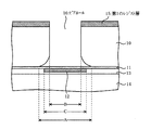
前記ビアホールを形成する工程の前記半導体基板のエッチング時にオーバーエッチングすることで、前記ビアホールの底部の開口径が前記ビアホールの深さの途中における開口径よりも大きく、前記ビアホールの底部の開口径が前記金属層の平面的な幅よりも大きくなるように行われることを特徴とする半導体装置の製造方法。 - 第1の絶縁膜上に金属層が形成された半導体基板をエッチングして、当該半導体基板の裏面の当該金属層に対応する位置から当該半導体基板の当該表面に貫通するビアホールを形成する工程と、
前記ビアホールの底部で露出する第1の絶縁膜をエッチングして金属層を露出する工程と、
前記ビアホール内を含む前記半導体基板の裏面上に、当該ビアホールの底部で前記金属層を露出する第2の絶縁膜を形成する工程と、
前記ビアホール内で前記金属層と電気的に接続された貫通電極、及び当該貫通電極と電気的に接続された前記半導体基板の裏面の第2の絶縁膜上に延びる配線層を形成する工程と、
前記貫通電極上及び前記配線層上を含む前記半導体基板の裏面上に、当該配線層の一部を露出する保護層を形成する工程と、
前記半導体基板を複数の半導体チップに切断分離する工程と、を有し、
前記ビアホールを形成する工程の前記半導体基板のエッチング時にオーバーエッチングすることで、前記ビアホールの底部の開口径が前記ビアホールの深さの途中における開口径よりも大きく、前記ビアホールの底部の開口端部が前記金属層上に形成されない領域を有するように行われることを特徴とする半導体装置の製造方法。 - 第1の絶縁膜上に金属層が形成された半導体基板をエッチングして、当該半導体基板の裏面の当該金属層に対応する位置から当該半導体基板の当該表面に貫通するビアホールを形成する工程と、
前記ビアホールの底部で露出する第1の絶縁膜をエッチングして金属層を露出する工程と、
前記ビアホール内を含む前記半導体基板の裏面上に、当該ビアホールの底部で前記金属層を露出する第2の絶縁膜を形成する工程と、
前記ビアホール内で前記金属層と電気的に接続された貫通電極を形成する工程と、
前記半導体基板を複数の半導体チップに切断分離する工程と、を有し、
前記ビアホールを形成する工程の前記半導体基板のエッチング時にオーバーエッチングすることで、前記ビアホールの底部の開口径が前記ビアホールの深さの途中における開口径よりも大きく、前記ビアホールの底部の開口径が前記金属層の平面的な幅よりも大きくなるように行われることを特徴とする半導体装置の製造方法。 - 第1の絶縁膜上に金属層が形成された半導体基板をエッチングして、当該半導体基板の裏面の当該金属層に対応する位置から当該半導体基板の当該表面に貫通するビアホールを形成する工程と、
前記ビアホールの底部で露出する第1の絶縁膜をエッチングして金属層を露出する工程と、
前記ビアホール内を含む前記半導体基板の裏面上に、当該ビアホールの底部で前記金属層を露出する第2の絶縁膜を形成する工程と、
前記ビアホール内で前記金属層と電気的に接続された貫通電極を形成する工程と、
前記半導体基板を複数の半導体チップに切断分離する工程と、を有し、
前記ビアホールを形成する工程の前記半導体基板のエッチング時にオーバーエッチングすることで、前記ビアホールの底部の開口径が前記ビアホールの深さの途中における開口径よりも大きく、前記ビアホールの底部の開口端部が前記金属層上に形成されない領域を有するように行われることを特徴とする半導体装置の製造方法。 - 前記配線層の一部上に導電端子を形成する工程を有することを特徴とする請求項1または請求項2に記載の半導体装置の製造方法。
- 前記半導体基板上に支持体を貼り付ける工程を有することを特徴とする請求項1乃至請求項5のいずれか1項に記載の半導体装置の製造方法。
Priority Applications (7)
| Application Number | Priority Date | Filing Date | Title |
|---|---|---|---|
| JP2004310726A JP4443379B2 (ja) | 2004-10-26 | 2004-10-26 | 半導体装置の製造方法 |
| TW094135828A TWI267132B (en) | 2004-10-26 | 2005-10-14 | Semiconductor device and manufacturing method of the same |
| CNB2005101180996A CN100429770C (zh) | 2004-10-26 | 2005-10-25 | 半导体装置及其制造方法 |
| US11/257,390 US7339273B2 (en) | 2004-10-26 | 2005-10-25 | Semiconductor device with a via hole having a diameter at the surface larger than a width of a pad electrode |
| KR1020050100580A KR100647760B1 (ko) | 2004-10-26 | 2005-10-25 | 반도체 장치 및 그 제조 방법 |
| EP05023409A EP1653509A3 (en) | 2004-10-26 | 2005-10-26 | Semiconductor device and manufacturing method of the same |
| US11/969,065 US7670955B2 (en) | 2004-10-26 | 2008-01-03 | Semiconductor device and manufacturing method of the same |
Applications Claiming Priority (1)
| Application Number | Priority Date | Filing Date | Title |
|---|---|---|---|
| JP2004310726A JP4443379B2 (ja) | 2004-10-26 | 2004-10-26 | 半導体装置の製造方法 |
Related Child Applications (1)
| Application Number | Title | Priority Date | Filing Date |
|---|---|---|---|
| JP2009259715A Division JP5258735B2 (ja) | 2009-11-13 | 2009-11-13 | 半導体装置 |
Publications (2)
| Publication Number | Publication Date |
|---|---|
| JP2006128172A JP2006128172A (ja) | 2006-05-18 |
| JP4443379B2 true JP4443379B2 (ja) | 2010-03-31 |
Family
ID=35385569
Family Applications (1)
| Application Number | Title | Priority Date | Filing Date |
|---|---|---|---|
| JP2004310726A Expired - Fee Related JP4443379B2 (ja) | 2004-10-26 | 2004-10-26 | 半導体装置の製造方法 |
Country Status (6)
| Country | Link |
|---|---|
| US (2) | US7339273B2 (ja) |
| EP (1) | EP1653509A3 (ja) |
| JP (1) | JP4443379B2 (ja) |
| KR (1) | KR100647760B1 (ja) |
| CN (1) | CN100429770C (ja) |
| TW (1) | TWI267132B (ja) |
Families Citing this family (45)
| Publication number | Priority date | Publication date | Assignee | Title |
|---|---|---|---|---|
| JP4850392B2 (ja) * | 2004-02-17 | 2012-01-11 | 三洋電機株式会社 | 半導体装置の製造方法 |
| JP4443379B2 (ja) * | 2004-10-26 | 2010-03-31 | 三洋電機株式会社 | 半導体装置の製造方法 |
| TWI303864B (en) * | 2004-10-26 | 2008-12-01 | Sanyo Electric Co | Semiconductor device and method for making the same |
| JP4873517B2 (ja) * | 2004-10-28 | 2012-02-08 | オンセミコンダクター・トレーディング・リミテッド | 半導体装置及びその製造方法 |
| US7485967B2 (en) | 2005-03-10 | 2009-02-03 | Sanyo Electric Co., Ltd. | Semiconductor device with via hole for electric connection |
| TWI269419B (en) * | 2005-06-09 | 2006-12-21 | Advanced Semiconductor Eng | Method for forming wafer-level heat spreader structure and packaging structure thereof |
| JP2007150083A (ja) * | 2005-11-29 | 2007-06-14 | Elpida Memory Inc | 半導体装置の製造方法 |
| KR100884238B1 (ko) * | 2006-05-22 | 2009-02-17 | 삼성전자주식회사 | 앵커형 결합 구조를 갖는 반도체 패키지 및 그 제조 방법 |
| JP4773307B2 (ja) * | 2006-09-15 | 2011-09-14 | Okiセミコンダクタ株式会社 | 半導体装置の製造方法 |
| JP4979320B2 (ja) * | 2006-09-28 | 2012-07-18 | ルネサスエレクトロニクス株式会社 | 半導体ウェハおよびその製造方法、ならびに半導体装置の製造方法 |
| US8212331B1 (en) * | 2006-10-02 | 2012-07-03 | Newport Fab, Llc | Method for fabricating a backside through-wafer via in a processed wafer and related structure |
| JP5242070B2 (ja) * | 2007-03-29 | 2013-07-24 | 株式会社フジクラ | 貫通配線基板 |
| JP4585561B2 (ja) * | 2007-09-04 | 2010-11-24 | 株式会社東芝 | 半導体装置の製造方法 |
| TWI331488B (en) * | 2007-10-09 | 2010-10-01 | Unimicron Technology Corp | Printed circuit board and fabrication method thereof |
| US7566637B2 (en) * | 2007-12-13 | 2009-07-28 | International Business Machines Corporation | Method of inhibition of metal diffusion arising from laser dicing |
| JP5259197B2 (ja) * | 2008-01-09 | 2013-08-07 | ソニー株式会社 | 半導体装置及びその製造方法 |
| DE102008033395B3 (de) * | 2008-07-16 | 2010-02-04 | Austriamicrosystems Ag | Verfahren zur Herstellung eines Halbleiterbauelementes und Halbleiterbauelement |
| JP5242282B2 (ja) * | 2008-07-31 | 2013-07-24 | 株式会社東芝 | 半導体装置とその製造方法 |
| US7906404B2 (en) * | 2008-11-21 | 2011-03-15 | Teledyne Scientific & Imaging, Llc | Power distribution for CMOS circuits using in-substrate decoupling capacitors and back side metal layers |
| US8343806B2 (en) | 2009-03-05 | 2013-01-01 | Raytheon Company | Hermetic packaging of integrated circuit components |
| US20100258952A1 (en) * | 2009-04-08 | 2010-10-14 | Interconnect Portfolio Llc | Interconnection of IC Chips by Flex Circuit Superstructure |
| DE102009049102B4 (de) * | 2009-10-13 | 2012-10-04 | Austriamicrosystems Ag | Halbleiterbauelement mit Durchkontaktierung und Verfahren zur Herstellung einer Durchkontaktierung in einem Halbleiterbauelement |
| JP5532394B2 (ja) | 2009-10-15 | 2014-06-25 | セイコーエプソン株式会社 | 半導体装置及び回路基板並びに電子機器 |
| US8207615B2 (en) * | 2010-01-20 | 2012-06-26 | Bai-Yao Lou | Chip package and method for fabricating the same |
| CN102148202B (zh) * | 2010-02-09 | 2016-06-08 | 精材科技股份有限公司 | 晶片封装体及其形成方法 |
| JP5730654B2 (ja) * | 2010-06-24 | 2015-06-10 | 新光電気工業株式会社 | 配線基板及びその製造方法 |
| US9190325B2 (en) * | 2010-09-30 | 2015-11-17 | Taiwan Semiconductor Manufacturing Company, Ltd. | TSV formation |
| US8901701B2 (en) * | 2011-02-10 | 2014-12-02 | Chia-Sheng Lin | Chip package and fabrication method thereof |
| TWI485818B (zh) * | 2011-06-16 | 2015-05-21 | 精材科技股份有限公司 | 晶片封裝體及其形成方法 |
| CN102891120B (zh) * | 2011-07-22 | 2016-06-08 | 精材科技股份有限公司 | 晶片封装体及其形成方法 |
| US8816505B2 (en) * | 2011-07-29 | 2014-08-26 | Tessera, Inc. | Low stress vias |
| JP5832852B2 (ja) | 2011-10-21 | 2015-12-16 | 浜松ホトニクス株式会社 | 光検出装置 |
| JP5791461B2 (ja) | 2011-10-21 | 2015-10-07 | 浜松ホトニクス株式会社 | 光検出装置 |
| RU2546856C2 (ru) * | 2013-05-28 | 2015-04-10 | Закрытое акционерное общество "НИИМП-Т" | Способ изготовления полупроводниковых свч приборов |
| US10727122B2 (en) | 2014-12-08 | 2020-07-28 | International Business Machines Corporation | Self-aligned via interconnect structures |
| JP6269703B2 (ja) | 2016-02-24 | 2018-01-31 | トヨタ自動車株式会社 | 車両用動力伝達装置の油圧制御装置 |
| JP6282307B2 (ja) * | 2016-06-01 | 2018-02-21 | 浜松ホトニクス株式会社 | 半導体光検出素子 |
| US9893083B1 (en) * | 2016-10-13 | 2018-02-13 | Micron Technology, Inc. | Elevationally-extending strings of memory cells individually comprising a programmable charge storage transistor and methods of processing silicon nitride-comprising materials |
| US20180122749A1 (en) * | 2016-11-01 | 2018-05-03 | Advanced Semiconductor Engineering, Inc. | Semiconductor wafer, semiconductor package and method for manufacturing the same |
| EP3460835B1 (en) * | 2017-09-20 | 2020-04-01 | ams AG | Method for manufacturing a semiconductor device and semiconductor device |
| US11749790B2 (en) | 2017-12-20 | 2023-09-05 | Lumileds Llc | Segmented LED with embedded transistors |
| CN110739269B (zh) * | 2019-10-25 | 2020-11-20 | 武汉新芯集成电路制造有限公司 | 半导体器件及其形成方法 |
| US11482506B2 (en) * | 2020-03-31 | 2022-10-25 | Taiwan Semiconductor Manufacturing Company Limited | Edge-trimming methods for wafer bonding and dicing |
| CN113539945B (zh) | 2020-04-16 | 2023-09-29 | 长鑫存储技术有限公司 | 半导体结构及其形成方法 |
| US12628640B2 (en) | 2021-06-24 | 2026-05-12 | Intel Corporation | Metal line profile shaping for advanced integrated circuit structure fabrication |
Family Cites Families (71)
| Publication number | Priority date | Publication date | Assignee | Title |
|---|---|---|---|---|
| US4097890A (en) | 1976-06-23 | 1978-06-27 | Hewlett-Packard Company | Low parasitic capacitance and resistance beamlead semiconductor component and method of manufacture |
| FR2637151A1 (fr) | 1988-09-29 | 1990-03-30 | Commissariat Energie Atomique | Procede de realisation de connexions electriques a travers un substrat |
| US5056216A (en) | 1990-01-26 | 1991-10-15 | Sri International | Method of forming a plurality of solder connections |
| US5229647A (en) * | 1991-03-27 | 1993-07-20 | Micron Technology, Inc. | High density data storage using stacked wafers |
| US5149674A (en) * | 1991-06-17 | 1992-09-22 | Motorola, Inc. | Method for making a planar multi-layer metal bonding pad |
| JPH0817186B2 (ja) * | 1992-03-18 | 1996-02-21 | 三星電子株式会社 | 電界効果トランジスタの製造方法 |
| US5248903A (en) | 1992-09-18 | 1993-09-28 | Lsi Logic Corporation | Composite bond pads for semiconductor devices |
| US5432119A (en) * | 1994-01-31 | 1995-07-11 | Hughes Aircraft Company | High yield electron-beam gate fabrication method for sub-micron gate FETS |
| WO1996013062A1 (en) | 1994-10-19 | 1996-05-02 | Ceram Incorporated | Apparatus and method of manufacturing stacked wafer array |
| US6204074B1 (en) * | 1995-01-09 | 2001-03-20 | International Business Machines Corporation | Chip design process for wire bond and flip-chip package |
| JPH08293523A (ja) | 1995-02-21 | 1996-11-05 | Seiko Epson Corp | 半導体装置およびその製造方法 |
| JPH09321175A (ja) * | 1996-05-30 | 1997-12-12 | Oki Electric Ind Co Ltd | マイクロ波回路及びチップ |
| DE69730629T2 (de) | 1996-12-26 | 2005-02-03 | Matsushita Electric Industrial Co., Ltd., Kadoma | Leiterplatte und Elektronikkomponente |
| US5910687A (en) | 1997-01-24 | 1999-06-08 | Chipscale, Inc. | Wafer fabrication of die-bottom contacts for electronic devices |
| EP0860876A3 (de) | 1997-02-21 | 1999-09-22 | DaimlerChrysler AG | Anordnung und Verfahren zur Herstellung von CSP-Gehäusen für elektrische Bauteile |
| US5915167A (en) | 1997-04-04 | 1999-06-22 | Elm Technology Corporation | Three dimensional structure memory |
| JP3724110B2 (ja) | 1997-04-24 | 2005-12-07 | 三菱電機株式会社 | 半導体装置の製造方法 |
| US5985749A (en) * | 1997-06-25 | 1999-11-16 | Vlsi Technology, Inc. | Method of forming a via hole structure including CVD tungsten silicide barrier layer |
| IL123207A0 (en) | 1998-02-06 | 1998-09-24 | Shellcase Ltd | Integrated circuit device |
| JP2974022B1 (ja) | 1998-10-01 | 1999-11-08 | ヤマハ株式会社 | 半導体装置のボンディングパッド構造 |
| JP3382549B2 (ja) * | 1998-11-02 | 2003-03-04 | キヤノン株式会社 | 半導体装置及びアクティブマトリクス基板 |
| TW442873B (en) | 1999-01-14 | 2001-06-23 | United Microelectronics Corp | Three-dimension stack-type chip structure and its manufacturing method |
| US6110816A (en) | 1999-03-05 | 2000-08-29 | Taiwan Semiconductor Manufacturing Company | Method for improving bondability for deep-submicron integrated circuit package |
| US6031293A (en) * | 1999-04-26 | 2000-02-29 | United Microelectronics Corporation | Package-free bonding pad structure |
| US6300670B1 (en) | 1999-07-26 | 2001-10-09 | Stmicroelectronics, Inc. | Backside bus vias |
| JP3468188B2 (ja) * | 2000-01-24 | 2003-11-17 | ヤマハ株式会社 | 半導体装置とその製法 |
| JP3629178B2 (ja) * | 2000-02-21 | 2005-03-16 | Necエレクトロニクス株式会社 | フリップチップ型半導体装置及びその製造方法 |
| JP3778256B2 (ja) | 2000-02-28 | 2006-05-24 | セイコーエプソン株式会社 | 半導体装置及びその製造方法、回路基板並びに電子機器 |
| JP3879816B2 (ja) * | 2000-06-02 | 2007-02-14 | セイコーエプソン株式会社 | 半導体装置及びその製造方法、積層型半導体装置、回路基板並びに電子機器 |
| JP4329235B2 (ja) * | 2000-06-27 | 2009-09-09 | セイコーエプソン株式会社 | 半導体装置及びその製造方法 |
| US6562709B1 (en) * | 2000-08-22 | 2003-05-13 | Charles W. C. Lin | Semiconductor chip assembly with simultaneously electroplated contact terminal and connection joint |
| US6512292B1 (en) * | 2000-09-12 | 2003-01-28 | International Business Machines Corporation | Semiconductor chip structures with embedded thermal conductors and a thermal sink disposed over opposing substrate surfaces |
| KR100366635B1 (ko) * | 2000-11-01 | 2003-01-09 | 삼성전자 주식회사 | 반도체 소자의 금속 배선 및 그 제조방법 |
| JP4771607B2 (ja) * | 2001-03-30 | 2011-09-14 | 富士通セミコンダクター株式会社 | 半導体装置及びその製造方法 |
| JP3530149B2 (ja) | 2001-05-21 | 2004-05-24 | 新光電気工業株式会社 | 配線基板の製造方法及び半導体装置 |
| JP2003045877A (ja) * | 2001-08-01 | 2003-02-14 | Sharp Corp | 半導体装置およびその製造方法 |
| US6734568B2 (en) | 2001-08-29 | 2004-05-11 | Kabushiki Kaisha Toshiba | Semiconductor device and method of manufacturing the same |
| JP4703061B2 (ja) * | 2001-08-30 | 2011-06-15 | 富士通株式会社 | 薄膜回路基板の製造方法およびビア形成基板の形成方法 |
| JP2003168818A (ja) * | 2001-09-18 | 2003-06-13 | Anritsu Corp | 順メサ型アバランシェフォトダイオード及びその製造方法 |
| JP3998984B2 (ja) * | 2002-01-18 | 2007-10-31 | 富士通株式会社 | 回路基板及びその製造方法 |
| US6960837B2 (en) | 2002-02-26 | 2005-11-01 | International Business Machines Corporation | Method of connecting core I/O pins to backside chip I/O pads |
| EP2560199B1 (en) | 2002-04-05 | 2016-08-03 | STMicroelectronics S.r.l. | Process for manufacturing a through insulated interconnection in a body of semiconductor material |
| JP4212293B2 (ja) | 2002-04-15 | 2009-01-21 | 三洋電機株式会社 | 半導体装置の製造方法 |
| TWI232560B (en) * | 2002-04-23 | 2005-05-11 | Sanyo Electric Co | Semiconductor device and its manufacture |
| JP2003318178A (ja) * | 2002-04-24 | 2003-11-07 | Seiko Epson Corp | 半導体装置及びその製造方法、回路基板並びに電子機器 |
| TWI229435B (en) | 2002-06-18 | 2005-03-11 | Sanyo Electric Co | Manufacture of semiconductor device |
| US6716737B2 (en) | 2002-07-29 | 2004-04-06 | Hewlett-Packard Development Company, L.P. | Method of forming a through-substrate interconnect |
| US6902872B2 (en) | 2002-07-29 | 2005-06-07 | Hewlett-Packard Development Company, L.P. | Method of forming a through-substrate interconnect |
| JP2004103761A (ja) * | 2002-09-09 | 2004-04-02 | Renesas Technology Corp | 半導体装置製造ライン |
| TWI227050B (en) | 2002-10-11 | 2005-01-21 | Sanyo Electric Co | Semiconductor device and method for manufacturing the same |
| TWI227550B (en) * | 2002-10-30 | 2005-02-01 | Sanyo Electric Co | Semiconductor device manufacturing method |
| JP2004186422A (ja) * | 2002-12-03 | 2004-07-02 | Shinko Electric Ind Co Ltd | 電子部品実装構造及びその製造方法 |
| JP4322508B2 (ja) | 2003-01-15 | 2009-09-02 | 新光電気工業株式会社 | 半導体装置の製造方法 |
| WO2004064159A1 (ja) | 2003-01-15 | 2004-07-29 | Fujitsu Limited | 半導体装置及び三次元実装半導体装置、並びに半導体装置の製造方法 |
| TWI239629B (en) * | 2003-03-17 | 2005-09-11 | Seiko Epson Corp | Method of manufacturing semiconductor device, semiconductor device, circuit substrate and electronic apparatus |
| JP3972846B2 (ja) | 2003-03-25 | 2007-09-05 | セイコーエプソン株式会社 | 半導体装置の製造方法 |
| JP2004311948A (ja) * | 2003-03-27 | 2004-11-04 | Seiko Epson Corp | 半導体装置、半導体デバイス、電子機器、および半導体装置の製造方法 |
| US7247939B2 (en) | 2003-04-01 | 2007-07-24 | Taiwan Semiconductor Manufacturing Co., Ltd. | Metal filled semiconductor features with improved structural stability |
| JP4130158B2 (ja) | 2003-06-09 | 2008-08-06 | 三洋電機株式会社 | 半導体装置の製造方法、半導体装置 |
| US7453158B2 (en) | 2003-07-31 | 2008-11-18 | Nvidia Corporation | Pad over active circuit system and method with meshed support structure |
| JP4323303B2 (ja) | 2003-12-17 | 2009-09-02 | 株式会社フジクラ | 基板の製造方法 |
| JP2005235860A (ja) | 2004-02-17 | 2005-09-02 | Sanyo Electric Co Ltd | 半導体装置及びその製造方法 |
| JP4850392B2 (ja) | 2004-02-17 | 2012-01-11 | 三洋電機株式会社 | 半導体装置の製造方法 |
| TWI249767B (en) | 2004-02-17 | 2006-02-21 | Sanyo Electric Co | Method for making a semiconductor device |
| JP4803964B2 (ja) | 2004-03-17 | 2011-10-26 | 三洋電機株式会社 | 電極構造 |
| JP4373866B2 (ja) * | 2004-07-16 | 2009-11-25 | 三洋電機株式会社 | 半導体装置の製造方法 |
| JP4376715B2 (ja) * | 2004-07-16 | 2009-12-02 | 三洋電機株式会社 | 半導体装置の製造方法 |
| JP4443379B2 (ja) * | 2004-10-26 | 2010-03-31 | 三洋電機株式会社 | 半導体装置の製造方法 |
| TWI303864B (en) * | 2004-10-26 | 2008-12-01 | Sanyo Electric Co | Semiconductor device and method for making the same |
| JP4873517B2 (ja) * | 2004-10-28 | 2012-02-08 | オンセミコンダクター・トレーディング・リミテッド | 半導体装置及びその製造方法 |
| US7485967B2 (en) * | 2005-03-10 | 2009-02-03 | Sanyo Electric Co., Ltd. | Semiconductor device with via hole for electric connection |
-
2004
- 2004-10-26 JP JP2004310726A patent/JP4443379B2/ja not_active Expired - Fee Related
-
2005
- 2005-10-14 TW TW094135828A patent/TWI267132B/zh not_active IP Right Cessation
- 2005-10-25 US US11/257,390 patent/US7339273B2/en not_active Expired - Lifetime
- 2005-10-25 CN CNB2005101180996A patent/CN100429770C/zh not_active Expired - Fee Related
- 2005-10-25 KR KR1020050100580A patent/KR100647760B1/ko not_active Expired - Fee Related
- 2005-10-26 EP EP05023409A patent/EP1653509A3/en not_active Withdrawn
-
2008
- 2008-01-03 US US11/969,065 patent/US7670955B2/en not_active Expired - Lifetime
Also Published As
| Publication number | Publication date |
|---|---|
| US7670955B2 (en) | 2010-03-02 |
| US7339273B2 (en) | 2008-03-04 |
| JP2006128172A (ja) | 2006-05-18 |
| CN1779961A (zh) | 2006-05-31 |
| TWI267132B (en) | 2006-11-21 |
| EP1653509A2 (en) | 2006-05-03 |
| US20060108695A1 (en) | 2006-05-25 |
| KR100647760B1 (ko) | 2006-11-23 |
| CN100429770C (zh) | 2008-10-29 |
| EP1653509A3 (en) | 2009-06-03 |
| US20080132038A1 (en) | 2008-06-05 |
| KR20060049324A (ko) | 2006-05-18 |
| TW200616055A (en) | 2006-05-16 |
Similar Documents
| Publication | Publication Date | Title |
|---|---|---|
| KR100647760B1 (ko) | 반도체 장치 및 그 제조 방법 | |
| JP4873517B2 (ja) | 半導体装置及びその製造方法 | |
| CN100428456C (zh) | 半导体装置及其制造方法 | |
| JP4850392B2 (ja) | 半導体装置の製造方法 | |
| JP4307284B2 (ja) | 半導体装置の製造方法 | |
| JP4376715B2 (ja) | 半導体装置の製造方法 | |
| JP4373866B2 (ja) | 半導体装置の製造方法 | |
| US7485967B2 (en) | Semiconductor device with via hole for electric connection | |
| KR100608184B1 (ko) | 반도체 장치 및 그 제조 방법 | |
| WO2003065450A2 (en) | Integrated circuits with backside contacts and methods for their fabrication | |
| JP4775007B2 (ja) | 半導体装置及びその製造方法 | |
| JP4845368B2 (ja) | 半導体装置及びその製造方法 | |
| JP4322181B2 (ja) | 半導体装置の製造方法 | |
| JP2010251791A (ja) | 半導体装置及びその製造方法 | |
| JP5036127B2 (ja) | 半導体装置の製造方法 | |
| JP5258735B2 (ja) | 半導体装置 | |
| JP2005260079A (ja) | 半導体装置及びその製造方法 | |
| JP4845986B2 (ja) | 半導体装置 |
Legal Events
| Date | Code | Title | Description |
|---|---|---|---|
| A621 | Written request for application examination |
Free format text: JAPANESE INTERMEDIATE CODE: A621 Effective date: 20071017 |
|
| A977 | Report on retrieval |
Free format text: JAPANESE INTERMEDIATE CODE: A971007 Effective date: 20090828 |
|
| A131 | Notification of reasons for refusal |
Free format text: JAPANESE INTERMEDIATE CODE: A131 Effective date: 20090918 |
|
| A521 | Request for written amendment filed |
Free format text: JAPANESE INTERMEDIATE CODE: A523 Effective date: 20091113 |
|
| TRDD | Decision of grant or rejection written | ||
| A01 | Written decision to grant a patent or to grant a registration (utility model) |
Free format text: JAPANESE INTERMEDIATE CODE: A01 Effective date: 20091214 |
|
| A01 | Written decision to grant a patent or to grant a registration (utility model) |
Free format text: JAPANESE INTERMEDIATE CODE: A01 |
|
| A61 | First payment of annual fees (during grant procedure) |
Free format text: JAPANESE INTERMEDIATE CODE: A61 Effective date: 20100112 |
|
| R151 | Written notification of patent or utility model registration |
Ref document number: 4443379 Country of ref document: JP Free format text: JAPANESE INTERMEDIATE CODE: R151 |
|
| FPAY | Renewal fee payment (event date is renewal date of database) |
Free format text: PAYMENT UNTIL: 20130122 Year of fee payment: 3 |
|
| R250 | Receipt of annual fees |
Free format text: JAPANESE INTERMEDIATE CODE: R250 |
|
| R250 | Receipt of annual fees |
Free format text: JAPANESE INTERMEDIATE CODE: R250 |
|
| R250 | Receipt of annual fees |
Free format text: JAPANESE INTERMEDIATE CODE: R250 |
|
| R250 | Receipt of annual fees |
Free format text: JAPANESE INTERMEDIATE CODE: R250 |
|
| R250 | Receipt of annual fees |
Free format text: JAPANESE INTERMEDIATE CODE: R250 |
|
| R250 | Receipt of annual fees |
Free format text: JAPANESE INTERMEDIATE CODE: R250 |
|
| R250 | Receipt of annual fees |
Free format text: JAPANESE INTERMEDIATE CODE: R250 |
|
| R250 | Receipt of annual fees |
Free format text: JAPANESE INTERMEDIATE CODE: R250 |
|
| R250 | Receipt of annual fees |
Free format text: JAPANESE INTERMEDIATE CODE: R250 |
|
| LAPS | Cancellation because of no payment of annual fees |