JP4457529B2 - Organic electroluminescence device - Google Patents
Organic electroluminescence device Download PDFInfo
- Publication number
- JP4457529B2 JP4457529B2 JP2001184804A JP2001184804A JP4457529B2 JP 4457529 B2 JP4457529 B2 JP 4457529B2 JP 2001184804 A JP2001184804 A JP 2001184804A JP 2001184804 A JP2001184804 A JP 2001184804A JP 4457529 B2 JP4457529 B2 JP 4457529B2
- Authority
- JP
- Japan
- Prior art keywords
- layer
- light emitting
- polymer
- organic
- group
- Prior art date
- Legal status (The legal status is an assumption and is not a legal conclusion. Google has not performed a legal analysis and makes no representation as to the accuracy of the status listed.)
- Expired - Fee Related
Links
- 238000005401 electroluminescence Methods 0.000 title claims description 28
- 239000000463 material Substances 0.000 claims description 57
- 229920000642 polymer Polymers 0.000 claims description 34
- 125000001424 substituent group Chemical group 0.000 claims description 7
- 125000004435 hydrogen atom Chemical group [H]* 0.000 claims description 4
- 239000010410 layer Substances 0.000 description 138
- 238000000034 method Methods 0.000 description 32
- 239000000872 buffer Substances 0.000 description 31
- 230000005525 hole transport Effects 0.000 description 27
- -1 hydroxyethyl group Chemical group 0.000 description 22
- 239000000203 mixture Substances 0.000 description 21
- 229910052757 nitrogen Inorganic materials 0.000 description 20
- 239000010408 film Substances 0.000 description 19
- 239000000975 dye Substances 0.000 description 15
- 229910052751 metal Inorganic materials 0.000 description 15
- 239000002184 metal Substances 0.000 description 15
- 238000002347 injection Methods 0.000 description 13
- 239000007924 injection Substances 0.000 description 13
- 229910052749 magnesium Inorganic materials 0.000 description 13
- 239000011777 magnesium Substances 0.000 description 13
- FYYHWMGAXLPEAU-UHFFFAOYSA-N Magnesium Chemical compound [Mg] FYYHWMGAXLPEAU-UHFFFAOYSA-N 0.000 description 12
- 238000007740 vapor deposition Methods 0.000 description 12
- 239000000758 substrate Substances 0.000 description 11
- 150000001875 compounds Chemical class 0.000 description 10
- 239000000126 substance Substances 0.000 description 10
- 239000007772 electrode material Substances 0.000 description 9
- 239000010409 thin film Substances 0.000 description 9
- 229910052782 aluminium Inorganic materials 0.000 description 8
- XAGFODPZIPBFFR-UHFFFAOYSA-N aluminium Chemical compound [Al] XAGFODPZIPBFFR-UHFFFAOYSA-N 0.000 description 8
- 125000003118 aryl group Chemical group 0.000 description 8
- 238000000151 deposition Methods 0.000 description 7
- BQCADISMDOOEFD-UHFFFAOYSA-N Silver Chemical compound [Ag] BQCADISMDOOEFD-UHFFFAOYSA-N 0.000 description 6
- PQXKHYXIUOZZFA-UHFFFAOYSA-M lithium fluoride Chemical compound [Li+].[F-] PQXKHYXIUOZZFA-UHFFFAOYSA-M 0.000 description 6
- 239000011159 matrix material Substances 0.000 description 6
- 125000004430 oxygen atom Chemical group O* 0.000 description 6
- 229910052709 silver Inorganic materials 0.000 description 6
- 239000004332 silver Substances 0.000 description 6
- 238000004528 spin coating Methods 0.000 description 6
- 125000004429 atom Chemical group 0.000 description 5
- 150000002894 organic compounds Chemical class 0.000 description 5
- 229920003227 poly(N-vinyl carbazole) Polymers 0.000 description 5
- 229910052761 rare earth metal Inorganic materials 0.000 description 5
- 150000002910 rare earth metals Chemical class 0.000 description 5
- 125000004434 sulfur atom Chemical group 0.000 description 5
- 238000001771 vacuum deposition Methods 0.000 description 5
- STTGYIUESPWXOW-UHFFFAOYSA-N 2,9-dimethyl-4,7-diphenyl-1,10-phenanthroline Chemical compound C=12C=CC3=C(C=4C=CC=CC=4)C=C(C)N=C3C2=NC(C)=CC=1C1=CC=CC=C1 STTGYIUESPWXOW-UHFFFAOYSA-N 0.000 description 4
- RTZKZFJDLAIYFH-UHFFFAOYSA-N Diethyl ether Chemical compound CCOCC RTZKZFJDLAIYFH-UHFFFAOYSA-N 0.000 description 4
- 125000000217 alkyl group Chemical group 0.000 description 4
- 125000006615 aromatic heterocyclic group Chemical group 0.000 description 4
- 238000005266 casting Methods 0.000 description 4
- 238000000576 coating method Methods 0.000 description 4
- 230000008021 deposition Effects 0.000 description 4
- 229910052738 indium Inorganic materials 0.000 description 4
- 238000004519 manufacturing process Methods 0.000 description 4
- 239000002861 polymer material Substances 0.000 description 4
- 239000002356 single layer Substances 0.000 description 4
- 238000004544 sputter deposition Methods 0.000 description 4
- 229910052717 sulfur Inorganic materials 0.000 description 4
- UHOVQNZJYSORNB-UHFFFAOYSA-N Benzene Chemical compound C1=CC=CC=C1 UHOVQNZJYSORNB-UHFFFAOYSA-N 0.000 description 3
- WHXSMMKQMYFTQS-UHFFFAOYSA-N Lithium Chemical compound [Li] WHXSMMKQMYFTQS-UHFFFAOYSA-N 0.000 description 3
- 150000003983 crown ethers Chemical class 0.000 description 3
- 239000002019 doping agent Substances 0.000 description 3
- 239000011521 glass Substances 0.000 description 3
- 238000010438 heat treatment Methods 0.000 description 3
- APFVFJFRJDLVQX-UHFFFAOYSA-N indium atom Chemical compound [In] APFVFJFRJDLVQX-UHFFFAOYSA-N 0.000 description 3
- 229910052744 lithium Inorganic materials 0.000 description 3
- 125000004433 nitrogen atom Chemical group N* 0.000 description 3
- 150000004866 oxadiazoles Chemical class 0.000 description 3
- TWNQGVIAIRXVLR-UHFFFAOYSA-N oxo(oxoalumanyloxy)alumane Chemical compound O=[Al]O[Al]=O TWNQGVIAIRXVLR-UHFFFAOYSA-N 0.000 description 3
- 125000001997 phenyl group Chemical group [H]C1=C([H])C([H])=C(*)C([H])=C1[H] 0.000 description 3
- 238000006862 quantum yield reaction Methods 0.000 description 3
- 229910052710 silicon Inorganic materials 0.000 description 3
- PJANXHGTPQOBST-UHFFFAOYSA-N stilbene Chemical compound C=1C=CC=CC=1C=CC1=CC=CC=C1 PJANXHGTPQOBST-UHFFFAOYSA-N 0.000 description 3
- DNTVTBIKSZRANH-UHFFFAOYSA-N 4-(4-aminophenyl)-3-(3-methylphenyl)aniline Chemical compound CC1=CC=CC(C=2C(=CC=C(N)C=2)C=2C=CC(N)=CC=2)=C1 DNTVTBIKSZRANH-UHFFFAOYSA-N 0.000 description 2
- IJGRMHOSHXDMSA-UHFFFAOYSA-N Atomic nitrogen Chemical compound N#N IJGRMHOSHXDMSA-UHFFFAOYSA-N 0.000 description 2
- 229920008347 Cellulose acetate propionate Polymers 0.000 description 2
- YLQBMQCUIZJEEH-UHFFFAOYSA-N Furan Chemical group C=1C=COC=1 YLQBMQCUIZJEEH-UHFFFAOYSA-N 0.000 description 2
- KFZMGEQAYNKOFK-UHFFFAOYSA-N Isopropanol Chemical compound CC(C)O KFZMGEQAYNKOFK-UHFFFAOYSA-N 0.000 description 2
- ZOKXTWBITQBERF-UHFFFAOYSA-N Molybdenum Chemical compound [Mo] ZOKXTWBITQBERF-UHFFFAOYSA-N 0.000 description 2
- OAICVXFJPJFONN-UHFFFAOYSA-N Phosphorus Chemical compound [P] OAICVXFJPJFONN-UHFFFAOYSA-N 0.000 description 2
- PJANXHGTPQOBST-VAWYXSNFSA-N Stilbene Natural products C=1C=CC=CC=1/C=C/C1=CC=CC=C1 PJANXHGTPQOBST-VAWYXSNFSA-N 0.000 description 2
- WYURNTSHIVDZCO-UHFFFAOYSA-N Tetrahydrofuran Chemical compound C1CCOC1 WYURNTSHIVDZCO-UHFFFAOYSA-N 0.000 description 2
- FZWLAAWBMGSTSO-UHFFFAOYSA-N Thiazole Chemical group C1=CSC=N1 FZWLAAWBMGSTSO-UHFFFAOYSA-N 0.000 description 2
- YTPLMLYBLZKORZ-UHFFFAOYSA-N Thiophene Chemical compound C=1C=CSC=1 YTPLMLYBLZKORZ-UHFFFAOYSA-N 0.000 description 2
- 229910045601 alloy Inorganic materials 0.000 description 2
- 239000000956 alloy Substances 0.000 description 2
- 150000004945 aromatic hydrocarbons Chemical group 0.000 description 2
- 230000004888 barrier function Effects 0.000 description 2
- 125000003785 benzimidazolyl group Chemical group N1=C(NC2=C1C=CC=C2)* 0.000 description 2
- 230000000903 blocking effect Effects 0.000 description 2
- 238000011088 calibration curve Methods 0.000 description 2
- 150000001721 carbon Chemical group 0.000 description 2
- 229910052799 carbon Inorganic materials 0.000 description 2
- 238000006243 chemical reaction Methods 0.000 description 2
- 230000000052 comparative effect Effects 0.000 description 2
- 229920001940 conductive polymer Polymers 0.000 description 2
- 239000000470 constituent Substances 0.000 description 2
- 229910052802 copper Inorganic materials 0.000 description 2
- 239000010949 copper Substances 0.000 description 2
- ZYGHJZDHTFUPRJ-UHFFFAOYSA-N coumarin Chemical compound C1=CC=C2OC(=O)C=CC2=C1 ZYGHJZDHTFUPRJ-UHFFFAOYSA-N 0.000 description 2
- 229910001873 dinitrogen Inorganic materials 0.000 description 2
- 238000005286 illumination Methods 0.000 description 2
- 125000002883 imidazolyl group Chemical group 0.000 description 2
- 238000005259 measurement Methods 0.000 description 2
- 150000002739 metals Chemical class 0.000 description 2
- 229910052750 molybdenum Inorganic materials 0.000 description 2
- 239000011733 molybdenum Substances 0.000 description 2
- 125000001624 naphthyl group Chemical group 0.000 description 2
- WCPAKWJPBJAGKN-UHFFFAOYSA-N oxadiazole Chemical group C1=CON=N1 WCPAKWJPBJAGKN-UHFFFAOYSA-N 0.000 description 2
- 125000003854 p-chlorophenyl group Chemical group [H]C1=C([H])C(*)=C([H])C([H])=C1Cl 0.000 description 2
- 125000001037 p-tolyl group Chemical group [H]C1=C([H])C(=C([H])C([H])=C1*)C([H])([H])[H] 0.000 description 2
- IEQIEDJGQAUEQZ-UHFFFAOYSA-N phthalocyanine Chemical compound N1C(N=C2C3=CC=CC=C3C(N=C3C4=CC=CC=C4C(=N4)N3)=N2)=C(C=CC=C2)C2=C1N=C1C2=CC=CC=C2C4=N1 IEQIEDJGQAUEQZ-UHFFFAOYSA-N 0.000 description 2
- 230000000704 physical effect Effects 0.000 description 2
- 239000002985 plastic film Substances 0.000 description 2
- 229920006255 plastic film Polymers 0.000 description 2
- 229920000139 polyethylene terephthalate Polymers 0.000 description 2
- 239000005020 polyethylene terephthalate Substances 0.000 description 2
- 229920000123 polythiophene Polymers 0.000 description 2
- 238000002360 preparation method Methods 0.000 description 2
- 125000003226 pyrazolyl group Chemical group 0.000 description 2
- 125000000168 pyrrolyl group Chemical group 0.000 description 2
- 125000001567 quinoxalinyl group Chemical class N1=C(C=NC2=CC=CC=C12)* 0.000 description 2
- 238000000926 separation method Methods 0.000 description 2
- 239000002904 solvent Substances 0.000 description 2
- 235000021286 stilbenes Nutrition 0.000 description 2
- QGKMIGUHVLGJBR-UHFFFAOYSA-M (4z)-1-(3-methylbutyl)-4-[[1-(3-methylbutyl)quinolin-1-ium-4-yl]methylidene]quinoline;iodide Chemical compound [I-].C12=CC=CC=C2N(CCC(C)C)C=CC1=CC1=CC=[N+](CCC(C)C)C2=CC=CC=C12 QGKMIGUHVLGJBR-UHFFFAOYSA-M 0.000 description 1
- SCYULBFZEHDVBN-UHFFFAOYSA-N 1,1-Dichloroethane Chemical compound CC(Cl)Cl SCYULBFZEHDVBN-UHFFFAOYSA-N 0.000 description 1
- 125000001399 1,2,3-triazolyl group Chemical group N1N=NC(=C1)* 0.000 description 1
- 125000001376 1,2,4-triazolyl group Chemical group N1N=C(N=C1)* 0.000 description 1
- MBIZXFATKUQOOA-UHFFFAOYSA-N 1,3,4-thiadiazole Chemical group C1=NN=CS1 MBIZXFATKUQOOA-UHFFFAOYSA-N 0.000 description 1
- JIHQDMXYYFUGFV-UHFFFAOYSA-N 1,3,5-triazine Chemical group C1=NC=NC=N1 JIHQDMXYYFUGFV-UHFFFAOYSA-N 0.000 description 1
- VERMWGQSKPXSPZ-BUHFOSPRSA-N 1-[(e)-2-phenylethenyl]anthracene Chemical class C=1C=CC2=CC3=CC=CC=C3C=C2C=1\C=C\C1=CC=CC=C1 VERMWGQSKPXSPZ-BUHFOSPRSA-N 0.000 description 1
- IANQTJSKSUMEQM-UHFFFAOYSA-N 1-benzofuran Chemical group C1=CC=C2OC=CC2=C1 IANQTJSKSUMEQM-UHFFFAOYSA-N 0.000 description 1
- FCEHBMOGCRZNNI-UHFFFAOYSA-N 1-benzothiophene Chemical group C1=CC=C2SC=CC2=C1 FCEHBMOGCRZNNI-UHFFFAOYSA-N 0.000 description 1
- SULWTXOWAFVWOY-PHEQNACWSA-N 2,3-bis[(E)-2-phenylethenyl]pyrazine Chemical class C=1C=CC=CC=1/C=C/C1=NC=CN=C1\C=C\C1=CC=CC=C1 SULWTXOWAFVWOY-PHEQNACWSA-N 0.000 description 1
- MVWPVABZQQJTPL-UHFFFAOYSA-N 2,3-diphenylcyclohexa-2,5-diene-1,4-dione Chemical class O=C1C=CC(=O)C(C=2C=CC=CC=2)=C1C1=CC=CC=C1 MVWPVABZQQJTPL-UHFFFAOYSA-N 0.000 description 1
- HONWGFNQCPRRFM-UHFFFAOYSA-N 2-n-(3-methylphenyl)-1-n,1-n,2-n-triphenylbenzene-1,2-diamine Chemical compound CC1=CC=CC(N(C=2C=CC=CC=2)C=2C(=CC=CC=2)N(C=2C=CC=CC=2)C=2C=CC=CC=2)=C1 HONWGFNQCPRRFM-UHFFFAOYSA-N 0.000 description 1
- MGADZUXDNSDTHW-UHFFFAOYSA-N 2H-pyran Chemical compound C1OC=CC=C1 MGADZUXDNSDTHW-UHFFFAOYSA-N 0.000 description 1
- AHDTYXOIJHCGKH-UHFFFAOYSA-N 4-[[4-(dimethylamino)-2-methylphenyl]-phenylmethyl]-n,n,3-trimethylaniline Chemical compound CC1=CC(N(C)C)=CC=C1C(C=1C(=CC(=CC=1)N(C)C)C)C1=CC=CC=C1 AHDTYXOIJHCGKH-UHFFFAOYSA-N 0.000 description 1
- MEIBOBDKQKIBJH-UHFFFAOYSA-N 4-methyl-n-[4-[1-[4-(4-methyl-n-(4-methylphenyl)anilino)phenyl]-4-phenylcyclohexyl]phenyl]-n-(4-methylphenyl)aniline Chemical compound C1=CC(C)=CC=C1N(C=1C=CC(=CC=1)C1(CCC(CC1)C=1C=CC=CC=1)C=1C=CC(=CC=1)N(C=1C=CC(C)=CC=1)C=1C=CC(C)=CC=1)C1=CC=C(C)C=C1 MEIBOBDKQKIBJH-UHFFFAOYSA-N 0.000 description 1
- ZOKIJILZFXPFTO-UHFFFAOYSA-N 4-methyl-n-[4-[1-[4-(4-methyl-n-(4-methylphenyl)anilino)phenyl]cyclohexyl]phenyl]-n-(4-methylphenyl)aniline Chemical compound C1=CC(C)=CC=C1N(C=1C=CC(=CC=1)C1(CCCCC1)C=1C=CC(=CC=1)N(C=1C=CC(C)=CC=1)C=1C=CC(C)=CC=1)C1=CC=C(C)C=C1 ZOKIJILZFXPFTO-UHFFFAOYSA-N 0.000 description 1
- DUSWRTUHJVJVRY-UHFFFAOYSA-N 4-methyl-n-[4-[2-[4-(4-methyl-n-(4-methylphenyl)anilino)phenyl]propan-2-yl]phenyl]-n-(4-methylphenyl)aniline Chemical compound C1=CC(C)=CC=C1N(C=1C=CC(=CC=1)C(C)(C)C=1C=CC(=CC=1)N(C=1C=CC(C)=CC=1)C=1C=CC(C)=CC=1)C1=CC=C(C)C=C1 DUSWRTUHJVJVRY-UHFFFAOYSA-N 0.000 description 1
- MVIXNQZIMMIGEL-UHFFFAOYSA-N 4-methyl-n-[4-[4-(4-methyl-n-(4-methylphenyl)anilino)phenyl]phenyl]-n-(4-methylphenyl)aniline Chemical group C1=CC(C)=CC=C1N(C=1C=CC(=CC=1)C=1C=CC(=CC=1)N(C=1C=CC(C)=CC=1)C=1C=CC(C)=CC=1)C1=CC=C(C)C=C1 MVIXNQZIMMIGEL-UHFFFAOYSA-N 0.000 description 1
- XIQGFRHAIQHZBD-UHFFFAOYSA-N 4-methyl-n-[4-[[4-(4-methyl-n-(4-methylphenyl)anilino)phenyl]-phenylmethyl]phenyl]-n-(4-methylphenyl)aniline Chemical compound C1=CC(C)=CC=C1N(C=1C=CC(=CC=1)C(C=1C=CC=CC=1)C=1C=CC(=CC=1)N(C=1C=CC(C)=CC=1)C=1C=CC(C)=CC=1)C1=CC=C(C)C=C1 XIQGFRHAIQHZBD-UHFFFAOYSA-N 0.000 description 1
- KDCGOANMDULRCW-UHFFFAOYSA-N 7H-purine Chemical group N1=CNC2=NC=NC2=C1 KDCGOANMDULRCW-UHFFFAOYSA-N 0.000 description 1
- ZYASLTYCYTYKFC-UHFFFAOYSA-N 9-methylidenefluorene Chemical class C1=CC=C2C(=C)C3=CC=CC=C3C2=C1 ZYASLTYCYTYKFC-UHFFFAOYSA-N 0.000 description 1
- VIJYEGDOKCKUOL-UHFFFAOYSA-N 9-phenylcarbazole Chemical compound C1=CC=CC=C1N1C2=CC=CC=C2C2=CC=CC=C21 VIJYEGDOKCKUOL-UHFFFAOYSA-N 0.000 description 1
- WKBOTKDWSSQWDR-UHFFFAOYSA-N Bromine atom Chemical compound [Br] WKBOTKDWSSQWDR-UHFFFAOYSA-N 0.000 description 1
- 229920002284 Cellulose triacetate Polymers 0.000 description 1
- 229910052684 Cerium Inorganic materials 0.000 description 1
- ZAMOUSCENKQFHK-UHFFFAOYSA-N Chlorine atom Chemical compound [Cl] ZAMOUSCENKQFHK-UHFFFAOYSA-N 0.000 description 1
- 241000284156 Clerodendrum quadriloculare Species 0.000 description 1
- RYGMFSIKBFXOCR-UHFFFAOYSA-N Copper Chemical compound [Cu] RYGMFSIKBFXOCR-UHFFFAOYSA-N 0.000 description 1
- 229910052692 Dysprosium Inorganic materials 0.000 description 1
- 229910052691 Erbium Inorganic materials 0.000 description 1
- 229910052693 Europium Inorganic materials 0.000 description 1
- PXGOKWXKJXAPGV-UHFFFAOYSA-N Fluorine Chemical compound FF PXGOKWXKJXAPGV-UHFFFAOYSA-N 0.000 description 1
- 229910052688 Gadolinium Inorganic materials 0.000 description 1
- 229910052689 Holmium Inorganic materials 0.000 description 1
- DGAQECJNVWCQMB-PUAWFVPOSA-M Ilexoside XXIX Chemical compound C[C@@H]1CC[C@@]2(CC[C@@]3(C(=CC[C@H]4[C@]3(CC[C@@H]5[C@@]4(CC[C@@H](C5(C)C)OS(=O)(=O)[O-])C)C)[C@@H]2[C@]1(C)O)C)C(=O)O[C@H]6[C@@H]([C@H]([C@@H]([C@H](O6)CO)O)O)O.[Na+] DGAQECJNVWCQMB-PUAWFVPOSA-M 0.000 description 1
- 229910000799 K alloy Inorganic materials 0.000 description 1
- PAYRUJLWNCNPSJ-UHFFFAOYSA-N N-phenyl amine Natural products NC1=CC=CC=C1 PAYRUJLWNCNPSJ-UHFFFAOYSA-N 0.000 description 1
- 229910052779 Neodymium Inorganic materials 0.000 description 1
- CBENFWSGALASAD-UHFFFAOYSA-N Ozone Chemical compound [O-][O+]=O CBENFWSGALASAD-UHFFFAOYSA-N 0.000 description 1
- 239000004696 Poly ether ether ketone Substances 0.000 description 1
- 229920012266 Poly(ether sulfone) PES Polymers 0.000 description 1
- 239000004697 Polyetherimide Substances 0.000 description 1
- 239000004642 Polyimide Substances 0.000 description 1
- 239000004734 Polyphenylene sulfide Substances 0.000 description 1
- 239000004793 Polystyrene Substances 0.000 description 1
- 229910052777 Praseodymium Inorganic materials 0.000 description 1
- JUJWROOIHBZHMG-UHFFFAOYSA-N Pyridine Chemical group C1=CC=NC=C1 JUJWROOIHBZHMG-UHFFFAOYSA-N 0.000 description 1
- 229910052772 Samarium Inorganic materials 0.000 description 1
- BUGBHKTXTAQXES-UHFFFAOYSA-N Selenium Chemical group [Se] BUGBHKTXTAQXES-UHFFFAOYSA-N 0.000 description 1
- XUIMIQQOPSSXEZ-UHFFFAOYSA-N Silicon Chemical group [Si] XUIMIQQOPSSXEZ-UHFFFAOYSA-N 0.000 description 1
- 229910052771 Terbium Inorganic materials 0.000 description 1
- 229910052775 Thulium Inorganic materials 0.000 description 1
- RTAQQCXQSZGOHL-UHFFFAOYSA-N Titanium Chemical group [Ti] RTAQQCXQSZGOHL-UHFFFAOYSA-N 0.000 description 1
- 239000007983 Tris buffer Substances 0.000 description 1
- 229910052769 Ytterbium Inorganic materials 0.000 description 1
- NNLVGZFZQQXQNW-ADJNRHBOSA-N [(2r,3r,4s,5r,6s)-4,5-diacetyloxy-3-[(2s,3r,4s,5r,6r)-3,4,5-triacetyloxy-6-(acetyloxymethyl)oxan-2-yl]oxy-6-[(2r,3r,4s,5r,6s)-4,5,6-triacetyloxy-2-(acetyloxymethyl)oxan-3-yl]oxyoxan-2-yl]methyl acetate Chemical compound O([C@@H]1O[C@@H]([C@H]([C@H](OC(C)=O)[C@H]1OC(C)=O)O[C@H]1[C@@H]([C@@H](OC(C)=O)[C@H](OC(C)=O)[C@@H](COC(C)=O)O1)OC(C)=O)COC(=O)C)[C@@H]1[C@@H](COC(C)=O)O[C@@H](OC(C)=O)[C@H](OC(C)=O)[C@H]1OC(C)=O NNLVGZFZQQXQNW-ADJNRHBOSA-N 0.000 description 1
- XHCLAFWTIXFWPH-UHFFFAOYSA-N [O-2].[O-2].[O-2].[O-2].[O-2].[V+5].[V+5] Chemical compound [O-2].[O-2].[O-2].[O-2].[O-2].[V+5].[V+5] XHCLAFWTIXFWPH-UHFFFAOYSA-N 0.000 description 1
- 150000001339 alkali metal compounds Chemical class 0.000 description 1
- 150000001341 alkaline earth metal compounds Chemical class 0.000 description 1
- 125000003545 alkoxy group Chemical group 0.000 description 1
- 229910003481 amorphous carbon Inorganic materials 0.000 description 1
- 150000008425 anthrones Chemical class 0.000 description 1
- 150000004982 aromatic amines Chemical class 0.000 description 1
- 125000003710 aryl alkyl group Chemical group 0.000 description 1
- 125000004104 aryloxy group Chemical group 0.000 description 1
- 125000005605 benzo group Chemical group 0.000 description 1
- 125000001164 benzothiazolyl group Chemical group S1C(=NC2=C1C=CC=C2)* 0.000 description 1
- 125000004541 benzoxazolyl group Chemical group O1C(=NC2=C1C=CC=C2)* 0.000 description 1
- 125000001797 benzyl group Chemical group [H]C1=C([H])C([H])=C(C([H])=C1[H])C([H])([H])* 0.000 description 1
- 239000011230 binding agent Substances 0.000 description 1
- 230000015572 biosynthetic process Effects 0.000 description 1
- 239000004305 biphenyl Substances 0.000 description 1
- GDTBXPJZTBHREO-UHFFFAOYSA-N bromine Substances BrBr GDTBXPJZTBHREO-UHFFFAOYSA-N 0.000 description 1
- 229910052794 bromium Inorganic materials 0.000 description 1
- 125000004106 butoxy group Chemical group [*]OC([H])([H])C([H])([H])C(C([H])([H])[H])([H])[H] 0.000 description 1
- 150000001718 carbodiimides Chemical class 0.000 description 1
- 239000010406 cathode material Substances 0.000 description 1
- HKQOBOMRSSHSTC-UHFFFAOYSA-N cellulose acetate Chemical compound OC1C(O)C(O)C(CO)OC1OC1C(CO)OC(O)C(O)C1O.CC(=O)OCC1OC(OC(C)=O)C(OC(C)=O)C(OC(C)=O)C1OC1C(OC(C)=O)C(OC(C)=O)C(OC(C)=O)C(COC(C)=O)O1.CCC(=O)OCC1OC(OC(=O)CC)C(OC(=O)CC)C(OC(=O)CC)C1OC1C(OC(=O)CC)C(OC(=O)CC)C(OC(=O)CC)C(COC(=O)CC)O1 HKQOBOMRSSHSTC-UHFFFAOYSA-N 0.000 description 1
- 239000000460 chlorine Substances 0.000 description 1
- 229910052801 chlorine Inorganic materials 0.000 description 1
- 238000004140 cleaning Methods 0.000 description 1
- 239000004020 conductor Substances 0.000 description 1
- 229920001577 copolymer Polymers 0.000 description 1
- 229960000956 coumarin Drugs 0.000 description 1
- 235000001671 coumarin Nutrition 0.000 description 1
- 239000013078 crystal Substances 0.000 description 1
- 125000004093 cyano group Chemical group *C#N 0.000 description 1
- 125000000753 cycloalkyl group Chemical group 0.000 description 1
- 125000000113 cyclohexyl group Chemical group [H]C1([H])C([H])([H])C([H])([H])C([H])(*)C([H])([H])C1([H])[H] 0.000 description 1
- 125000001511 cyclopentyl group Chemical group [H]C1([H])C([H])([H])C([H])([H])C([H])(*)C1([H])[H] 0.000 description 1
- DMBHHRLKUKUOEG-UHFFFAOYSA-N diphenylamine Chemical group C=1C=CC=CC=1NC1=CC=CC=C1 DMBHHRLKUKUOEG-UHFFFAOYSA-N 0.000 description 1
- 238000001035 drying Methods 0.000 description 1
- 230000000694 effects Effects 0.000 description 1
- 230000005684 electric field Effects 0.000 description 1
- 125000006575 electron-withdrawing group Chemical group 0.000 description 1
- 229920000775 emeraldine polymer Polymers 0.000 description 1
- 238000005516 engineering process Methods 0.000 description 1
- 125000005678 ethenylene group Chemical group [H]C([*:1])=C([H])[*:2] 0.000 description 1
- 125000001301 ethoxy group Chemical group [H]C([H])([H])C([H])([H])O* 0.000 description 1
- 125000001495 ethyl group Chemical group [H]C([H])([H])C([H])([H])* 0.000 description 1
- 230000001747 exhibiting effect Effects 0.000 description 1
- 150000008376 fluorenones Chemical class 0.000 description 1
- GNBHRKFJIUUOQI-UHFFFAOYSA-N fluorescein Chemical compound O1C(=O)C2=CC=CC=C2C21C1=CC=C(O)C=C1OC1=CC(O)=CC=C21 GNBHRKFJIUUOQI-UHFFFAOYSA-N 0.000 description 1
- 229910052731 fluorine Inorganic materials 0.000 description 1
- 239000011737 fluorine Substances 0.000 description 1
- 229910052733 gallium Inorganic materials 0.000 description 1
- 125000005843 halogen group Chemical group 0.000 description 1
- RBTKNAXYKSUFRK-UHFFFAOYSA-N heliogen blue Chemical compound [Cu].[N-]1C2=C(C=CC=C3)C3=C1N=C([N-]1)C3=CC=CC=C3C1=NC([N-]1)=C(C=CC=C3)C3=C1N=C([N-]1)C3=CC=CC=C3C1=N2 RBTKNAXYKSUFRK-UHFFFAOYSA-N 0.000 description 1
- 150000002391 heterocyclic compounds Chemical class 0.000 description 1
- 125000000623 heterocyclic group Chemical group 0.000 description 1
- 229940083761 high-ceiling diuretics pyrazolone derivative Drugs 0.000 description 1
- 150000007857 hydrazones Chemical class 0.000 description 1
- 150000002430 hydrocarbons Chemical group 0.000 description 1
- 150000002460 imidazoles Chemical class 0.000 description 1
- 229910003437 indium oxide Inorganic materials 0.000 description 1
- PJXISJQVUVHSOJ-UHFFFAOYSA-N indium(iii) oxide Chemical compound [O-2].[O-2].[O-2].[In+3].[In+3] PJXISJQVUVHSOJ-UHFFFAOYSA-N 0.000 description 1
- AMGQUBHHOARCQH-UHFFFAOYSA-N indium;oxotin Chemical compound [In].[Sn]=O AMGQUBHHOARCQH-UHFFFAOYSA-N 0.000 description 1
- 125000001041 indolyl group Chemical group 0.000 description 1
- 239000011261 inert gas Substances 0.000 description 1
- 150000002484 inorganic compounds Chemical class 0.000 description 1
- 229910010272 inorganic material Inorganic materials 0.000 description 1
- 229940079865 intestinal antiinfectives imidazole derivative Drugs 0.000 description 1
- PNDPGZBMCMUPRI-UHFFFAOYSA-N iodine Chemical compound II PNDPGZBMCMUPRI-UHFFFAOYSA-N 0.000 description 1
- 125000001449 isopropyl group Chemical group [H]C([H])([H])C([H])(*)C([H])([H])[H] 0.000 description 1
- 125000002183 isoquinolinyl group Chemical group C1(=NC=CC2=CC=CC=C12)* 0.000 description 1
- 150000002576 ketones Chemical class 0.000 description 1
- 239000002346 layers by function Substances 0.000 description 1
- ORUIBWPALBXDOA-UHFFFAOYSA-L magnesium fluoride Chemical compound [F-].[F-].[Mg+2] ORUIBWPALBXDOA-UHFFFAOYSA-L 0.000 description 1
- 229910001635 magnesium fluoride Inorganic materials 0.000 description 1
- 125000000956 methoxy group Chemical group [H]C([H])([H])O* 0.000 description 1
- 125000004184 methoxymethyl group Chemical group [H]C([H])([H])OC([H])([H])* 0.000 description 1
- 125000002496 methyl group Chemical group [H]C([H])([H])* 0.000 description 1
- IBHBKWKFFTZAHE-UHFFFAOYSA-N n-[4-[4-(n-naphthalen-1-ylanilino)phenyl]phenyl]-n-phenylnaphthalen-1-amine Chemical group C1=CC=CC=C1N(C=1C2=CC=CC=C2C=CC=1)C1=CC=C(C=2C=CC(=CC=2)N(C=2C=CC=CC=2)C=2C3=CC=CC=C3C=CC=2)C=C1 IBHBKWKFFTZAHE-UHFFFAOYSA-N 0.000 description 1
- AODWRBPUCXIRKB-UHFFFAOYSA-N naphthalene perylene Chemical group C1=CC=CC2=CC=CC=C21.C1=CC(C2=CC=CC=3C2=C2C=CC=3)=C3C2=CC=CC3=C1 AODWRBPUCXIRKB-UHFFFAOYSA-N 0.000 description 1
- 239000012044 organic layer Substances 0.000 description 1
- 239000013110 organic ligand Substances 0.000 description 1
- 150000007978 oxazole derivatives Chemical class 0.000 description 1
- 125000002971 oxazolyl group Chemical group 0.000 description 1
- 230000003647 oxidation Effects 0.000 description 1
- 238000007254 oxidation reaction Methods 0.000 description 1
- GPRIERYVMZVKTC-UHFFFAOYSA-N p-quaterphenyl Chemical group C1=CC=CC=C1C1=CC=C(C=2C=CC(=CC=2)C=2C=CC=CC=2)C=C1 GPRIERYVMZVKTC-UHFFFAOYSA-N 0.000 description 1
- 238000000059 patterning Methods 0.000 description 1
- 125000002080 perylenyl group Chemical group C1(=CC=C2C=CC=C3C4=CC=CC5=CC=CC(C1=C23)=C45)* 0.000 description 1
- CSHWQDPOILHKBI-UHFFFAOYSA-N peryrene Natural products C1=CC(C2=CC=CC=3C2=C2C=CC=3)=C3C2=CC=CC3=C1 CSHWQDPOILHKBI-UHFFFAOYSA-N 0.000 description 1
- 125000000951 phenoxy group Chemical group [H]C1=C([H])C([H])=C(O*)C([H])=C1[H] 0.000 description 1
- 150000004986 phenylenediamines Chemical class 0.000 description 1
- 238000000206 photolithography Methods 0.000 description 1
- 239000004033 plastic Substances 0.000 description 1
- 229920003023 plastic Polymers 0.000 description 1
- 229920000767 polyaniline Polymers 0.000 description 1
- 229920001230 polyarylate Polymers 0.000 description 1
- 239000004417 polycarbonate Substances 0.000 description 1
- 229920000515 polycarbonate Polymers 0.000 description 1
- 229920002530 polyetherether ketone Polymers 0.000 description 1
- 229920001601 polyetherimide Polymers 0.000 description 1
- 239000011112 polyethylene naphthalate Substances 0.000 description 1
- 229920001721 polyimide Polymers 0.000 description 1
- 229920000069 polyphenylene sulfide Polymers 0.000 description 1
- 229920002223 polystyrene Polymers 0.000 description 1
- BITYAPCSNKJESK-UHFFFAOYSA-N potassiosodium Chemical compound [Na].[K] BITYAPCSNKJESK-UHFFFAOYSA-N 0.000 description 1
- 125000003373 pyrazinyl group Chemical group 0.000 description 1
- JEXVQSWXXUJEMA-UHFFFAOYSA-N pyrazol-3-one Chemical class O=C1C=CN=N1 JEXVQSWXXUJEMA-UHFFFAOYSA-N 0.000 description 1
- 150000003219 pyrazolines Chemical class 0.000 description 1
- PBMFSQRYOILNGV-UHFFFAOYSA-N pyridazine Chemical group C1=CC=NN=C1 PBMFSQRYOILNGV-UHFFFAOYSA-N 0.000 description 1
- 125000004076 pyridyl group Chemical group 0.000 description 1
- 125000000714 pyrimidinyl group Chemical group 0.000 description 1
- WVIICGIFSIBFOG-UHFFFAOYSA-N pyrylium Chemical compound C1=CC=[O+]C=C1 WVIICGIFSIBFOG-UHFFFAOYSA-N 0.000 description 1
- 239000010453 quartz Substances 0.000 description 1
- MCJGNVYPOGVAJF-UHFFFAOYSA-N quinolin-8-ol Chemical class C1=CN=C2C(O)=CC=CC2=C1 MCJGNVYPOGVAJF-UHFFFAOYSA-N 0.000 description 1
- DLJHXMRDIWMMGO-UHFFFAOYSA-N quinolin-8-ol;zinc Chemical compound [Zn].C1=CN=C2C(O)=CC=CC2=C1.C1=CN=C2C(O)=CC=CC2=C1 DLJHXMRDIWMMGO-UHFFFAOYSA-N 0.000 description 1
- 125000002943 quinolinyl group Chemical group N1=C(C=CC2=CC=CC=C12)* 0.000 description 1
- 238000005215 recombination Methods 0.000 description 1
- 230000006798 recombination Effects 0.000 description 1
- 239000011347 resin Substances 0.000 description 1
- 229920005989 resin Polymers 0.000 description 1
- 239000001022 rhodamine dye Substances 0.000 description 1
- 150000003839 salts Chemical class 0.000 description 1
- 229910052711 selenium Inorganic materials 0.000 description 1
- 239000004065 semiconductor Substances 0.000 description 1
- VYPSYNLAJGMNEJ-UHFFFAOYSA-N silicon dioxide Inorganic materials O=[Si]=O VYPSYNLAJGMNEJ-UHFFFAOYSA-N 0.000 description 1
- 229910052708 sodium Inorganic materials 0.000 description 1
- 239000011734 sodium Substances 0.000 description 1
- 239000000243 solution Substances 0.000 description 1
- 239000010935 stainless steel Substances 0.000 description 1
- 229910001220 stainless steel Inorganic materials 0.000 description 1
- 229910052712 strontium Inorganic materials 0.000 description 1
- CIOAGBVUUVVLOB-UHFFFAOYSA-N strontium atom Chemical compound [Sr] CIOAGBVUUVVLOB-UHFFFAOYSA-N 0.000 description 1
- 125000005504 styryl group Chemical group 0.000 description 1
- 125000000542 sulfonic acid group Chemical group 0.000 description 1
- 229940042055 systemic antimycotics triazole derivative Drugs 0.000 description 1
- 229910052714 tellurium Inorganic materials 0.000 description 1
- PORWMNRCUJJQNO-UHFFFAOYSA-N tellurium atom Chemical group [Te] PORWMNRCUJJQNO-UHFFFAOYSA-N 0.000 description 1
- 125000000999 tert-butyl group Chemical group [H]C([H])([H])C(*)(C([H])([H])[H])C([H])([H])[H] 0.000 description 1
- 150000004867 thiadiazoles Chemical class 0.000 description 1
- 229930192474 thiophene Natural products 0.000 description 1
- IBBLKSWSCDAPIF-UHFFFAOYSA-N thiopyran Chemical compound S1C=CC=C=C1 IBBLKSWSCDAPIF-UHFFFAOYSA-N 0.000 description 1
- 229910052719 titanium Inorganic materials 0.000 description 1
- 238000002834 transmittance Methods 0.000 description 1
- 239000012780 transparent material Substances 0.000 description 1
- ILJSQTXMGCGYMG-UHFFFAOYSA-N triacetic acid Chemical compound CC(=O)CC(=O)CC(O)=O ILJSQTXMGCGYMG-UHFFFAOYSA-N 0.000 description 1
- 125000002023 trifluoromethyl group Chemical group FC(F)(F)* 0.000 description 1
- WFKWXMTUELFFGS-UHFFFAOYSA-N tungsten Chemical compound [W] WFKWXMTUELFFGS-UHFFFAOYSA-N 0.000 description 1
- 229910052721 tungsten Inorganic materials 0.000 description 1
- 239000010937 tungsten Substances 0.000 description 1
- 229910001935 vanadium oxide Inorganic materials 0.000 description 1
- 125000000391 vinyl group Chemical group [H]C([*])=C([H])[H] 0.000 description 1
- 229920002554 vinyl polymer Polymers 0.000 description 1
- 150000004798 β-ketoamides Chemical class 0.000 description 1
Landscapes
- Electroluminescent Light Sources (AREA)
Description
【0001】
【発明の属する技術分野】
本発明は、有機エレクトロルミネッセンス(以下有機ELと略記する場合もある)素子に関する。
【0002】
【従来の技術】
従来、発光型の電子ディスプレイデバイスとして、エレクトロルミネッセンスディスプレイ(ELD)がある。ELDの構成要素としては、無機エレクトロルミネッセンス素子や有機エレクトロルミネッセンス素子等が挙げられる。無機エレクトロルミネッセンス素子は平面型光源として使用されてきたが、発光素子を駆動させるためには交流の高電圧が必要である。有機エレクトロルミネッセンス素子は、発光する化合物を含有する発光層を、陰極と陽極で挟んだ構成を有し、発光層に電子及び正孔を注入して、再結合させることにより励起子(エキシトン)を生成させ、このエキシトンが失活する際の光の放出(蛍光・燐光)を利用して発光する素子であり、数V〜数十V程度の電圧で発光が可能であり、さらに、自己発光型であるために視野角に富み、視認性が高く、薄膜型の完全固体素子であるために省スペース、携帯性等の観点から注目されている。
【0003】
しかしながら、今後の実用化に向けた有機EL素子には、さらなる低消費電力で効率よく高輝度、長寿命に発光する有機EL素子の開発が望まれている。また、低コストな有機EL素子の開発が望まれている。又、有機化合物の蒸着操作を伴うエレクトロルミネッセンス素子は生産性に問題があり、製造工程の簡略化、加工性、大面積化の観点から塗布方式が望まれている。
【0004】
そこで、生産性に有利な塗布方式を用いるエレクトロルミネッセンス素子材料として、重合体素子が提案され、例えば、パラフェニレンビニレン系ポリマー等が知られているが(アドバンスドマテリアルズ,4項,1992年)、発光部がポリマー主鎖中にあるため、発光材料の濃度制御が難しく、色調、発光強度の微妙な制御が難しいという問題があった。
【0005】
同様に、塗布方式を用いるEL素子材料として、特開平4−212286号に記載のような、ポリN−ビニルカルバゾール中に低分子量色素を分散した素子が開示されている。この技術は、色素種、色素濃度を任意に変更できるため発光強度の調整が比較的容易であるという特徴を有するが、層分離が起こりやすく、また、均質な発光が得難いため、効率よく高輝度、長寿命に発光することに難点があった。更に、ポリN−ビニルカルバゾール自体のキャリア輸送能が低いために、高輝度かつ長寿命の発光を得にくいという問題点があった。
【0006】
【発明が解決しようとする課題】
本発明の目的は、発光輝度が高く、半減時間の長い(高寿命である)有機エレクトロルミネッセンス素子を提供することである。
【0007】
【課題を解決するための手段】
本発明の上記目的は、下記の項目1〜6により達成された。
【0008】
1.支持体上に、発光材料と前記一般式(1)で表される繰り返し単位を有する重合体を含有することを特徴とする有機エレクトロルミネッセンス素子。
【0009】
2.前記一般式(1)で表される繰り返し単位を有する重合体の数平均分子量が500以上300000以下であることを特徴とする前記1に記載の有機エレクトロルミネッセンス素子。
【0010】
3.支持体上に、発光材料と前記一般式(2)で表される繰り返し単位を有する重合体を含有することを特徴とする有機エレクトロルミネッセンス素子。
【0011】
4.前記一般式(2)で表される繰り返し単位を有する重合体の数平均分子量が500以上300000以下であることを特徴とする前記3に記載の有機エレクトロルミネッセンス素子。
【0012】
5.陰極、陽極および発光層を有し、該発光層が前記一般式(1)で表される繰り返し単位を有する重合体を含有することを特徴とする前記1または2に記載の有機エレクトロルミネッセンス素子。
【0013】
6.陰極、陽極および発光層を有し、該発光層が前記一般式(2)で表される繰り返し単位を有する重合体を含有することを特徴とする前記3または4に記載の有機エレクトロルミネッセンス素子。
【0014】
以下、本発明を詳細に説明する。
本発明者らは、上記記載の塗布方式を用いて作製した有機EL素子の問題点について種々の検討を行ない、キャリア輸送性の向上と層分離などを招来しない良好な膜物性を有するEL素子材料の探索の中で、種々の高分子化合物について検討を行った結果、ジフェニルアミン骨格を部分構造として有する縮合複素環化合物で、且つ、該フェニル部分が非共役の炭化水素環で縮合された化合物を繰り返し単位として有する、前記一般式(1)または前記一般式(2)で表されるオリゴマーまたはポリマーを用いることにより、高いキャリア輸送性と良好な膜物性の両方の特性を同時に満足する有機EL素子が得られることを見いだした。
【0015】
本発明に係る前記一般式(1)、一般式(2)で表される繰り返し単位を有する重合体について説明する。
【0016】
一般式(1)、一般式(2)で表される繰り返し単位において、R1〜R29で表される置換基としては例えば、ハロゲン原子(弗素、塩素、臭素、沃素等)、アルキル基(メチル基、エチル基、i−プロピル基、ヒドロキシエチル基、メトキシメチル基、トリフルオロメチル基、t−ブチル基等)、シクロアルキル基(シクロペンチル基、シクロヘキシル基等)、アラルキル基(ベンジル基、2−フェネチル基等)、アリール基(フェニル基、ナフチル基、p−トリル基、p−クロロフェニル基等)、アルコキシル基(メトキシ基、エトキシ基、i−プロポキシ基、ブトキシ基等)、アリールオキシ基(フェノキシ基等)、シアノ基、複素環基(ピロール基、ピロリジル基、ピラゾリル基、イミダゾリル基、ピリジル基、ベンゾイミダゾリル基、ベンゾチアゾリル基、ベンゾオキサゾリル基等)等が挙げられ、これらの基は更に置換されてもよい。
【0017】
一般式(1)、一般式(2)において、R1及びR17はアリール基または芳香族複素環基であることが好ましい。
【0018】
R1、R17で表されるアリール基としては、フェニル基、ナフチル基、p−トリル基、p−クロロフェニル基等が挙げられる。
【0019】
R1、R17で表される芳香族複素環基としては、フラン環、ピロール環、ピラゾール環、イミダゾール環、オキサゾール環、チアゾール環、1,2,3−オキサジアゾール環、1,2,3−トリアゾール環、1,2,4−トリアゾール環、1,3,4−チアジアゾール環、ピリジン環、ピリダジン環、ピリミジン環、ピラジン環、s−トリアジン環、ベンゾフラン環、インドール環、ベンゾチオフェン環、ベンズイミダゾール環、ベンゾチアゾール環、プリン環、キノリン環及びイソキノリン環等が挙げられる。
【0020】
上記の基は更に置換基を有していても良い。
本発明においては、一般式(1)で表される繰り返し単位を有する重合体の中でも、特に好ましく用いられるのは、前記一般式(2)で表される繰り返し単位を有する重合体である。
【0021】
本発明に係る一般式(1)、一般式(3)で表される繰り返し単位を有する各々の重合体の数平均分子量は、500〜300000であることが好ましく、特に好ましくは1000〜200000である。
【0022】
ここで、上記の数平均分子量は、下記に記載の測定機器及び測定条件下にて求めた。
【0023】
測定機器 :GPC装置HLC−8220GPC(東ソー(株)製)
カラム :TSKgelSuperHM−Mカラム
カラム温度:40℃
測定溶媒 :テトラヒドロフラン
流量 :0.6ml/分
検量線 :単分散ポリスチレンを使用して検量線を作成した。
【0024】
本発明に係る一般式(1)の繰り返し単位を有する重合体は、例えば、テトラヘドロン レターズ42巻、1437頁〜1439頁(2001年)に記載の方法を参照して合成出来る。
【0025】
以下に、本発明に係る一般式(1)の繰り返し単位を有する重合体の具体例を示すが、本発明はこれらに限定されない。また、例示化合物の数平均分子量を表1に示す。
【0026】
【化3】
【化4】
【化5】
【表1】
本発明において、有機エレクトロルミネッセンス素子の層構成は単層でも多層積層でもよく、例えば多層構成の場合には有機物以外の層(例えばフッ化リチウム層や無機金属塩の層、またはそれらを含有する層など)が任意の位置に配置されていてもよい。
【0031】
本発明の有機エレクトロルミネッセンス素子は、基本的には一対の電極の間に発光層を挾持し、必要に応じ、正孔輸送層や電子輸送層を介在させた構造を有することが好ましい。
【0032】
具体的な構成としては、
(a)陽極/発光層/陰極
(b)陽極/正孔輸送層/発光層/陰極
(c)陽極/発光層/電子輸送層/陰極
(d)陽極/正孔輸送層/発光層/電子輸送層/陰極
(e)陽極/正孔輸送層/発光層/陰極バッファー層/陰極
(f)陽極/正孔輸送層/発光層/電子輸送層/陰極バッファー層/陰極
などが具体的な構成例として挙げられる。
【0033】
上記発光層は電極または電子注入層、正孔注入層から注入されてくる電子および正孔が再結合して発光する層であり、発光する部分は発光層の層内であっても発光層と隣接層との界面であっても良い。
【0034】
発光層に使用される材料(以下、発光材料という)は、蛍光または燐光を発する有機化合物または錯体であることが好ましく、有機エレクトロルミネッセンス素子の発光層に使用される公知のものの中から任意のものを選択して用いることができる。このような発光材料は、主に有機化合物であり、所望の色調により例えばMacromol.Synth.,125巻,17〜25頁に記載の化合物が挙げられる。
【0035】
発光材料は発光性能の他に、前記の正孔注入機能や電子注入機能を併せ持っていても良く、後記の正孔注入材料や電子注入材料の殆どが発光材料としても使用できる。
【0036】
発光材料は高分子材料でも良く、さらに前記発光材料を高分子鎖に導入した、または前記発光材料を高分子の主鎖とした高分子材料を使用しても良い。
【0037】
また、発光層にはドーパント(ゲスト物質)を併用してもよく、エレクトロルミネッセンス素子のドーパントとして使用される公知のものの中から任意のものを選択して用いることができる。
【0038】
ドーパントの例としては、溶液状態で蛍光量子収率が高い蛍光性有機分子、または、希土類錯体系蛍光体が挙げられる。ここで、蛍光量子収率は10%以上、特に30%以上が好ましい。
【0039】
蛍光量子収率が高い蛍光性有機分子としては、例えばクマリン系色素、ピラン系色素、シアニン系色素、クロコニウム系色素、スクアリウム系色素、オキソベンツアントラセン系色素、フルオレセイン系色素、ローダミン系色素、ピリリウム系色素、ペリレン系色素、スチルベン系色素、ポリチオフェン系色素などが挙げられる。
【0040】
以下に、本発明で用いられる蛍光体有機分子の具体例を示すが、これらに限定されない。
【0041】
【化6】
本発明に用いられる希土類錯体系蛍光体としては、希土類金属としてCe、Pr、Nd、Pm、Sm、Eu、Gd、Tb、Dy、Ho、Er、Tm、Yb等を有するものが挙げられ、錯体を形成する有機配位子としては、芳香族系、非芳香族系のどちらでも良く、下記一般式(A)で表される化合物が好ましい。
【0043】
一般式(A) Xa−(Lx)−(Ly)n−(Lz)−Ya
式中、Lx、Ly、Lzはそれぞれ独立に2個以上の結合手を持つ原子を表わし、nは0または1を表わし、XaはLxの隣接位に配位可能な原子を有する置換基を表わし、YaはLzの隣接位に配位可能な原子を有する置換基を表わす。さらにXaの任意の部分とLxとは互いに縮合して環を形成してもよく、Yaの任意の部分とLzとは互いに縮合して環を形成してもよく、LxとLzとは互いに縮合して環を形成してもよく、さらに分子内に芳香族炭化水素環または芳香族複素環が少なくとも一つ存在する。ただし、Xa−(Lx)−(Ly)n−(Lz)−Yaがβ−ジケトン誘導体やβ−ケトエステル誘導体、β−ケトアミド誘導体または前記ケトンの酸素原子を硫黄原子または−N(R201)−に置き換えたもの、クラウンエーテルやアザクラウンエーテルまたはチアクラウンエーテルまたはクラウンエーテルの酸素原子を任意の数硫黄原子または−N(R201)−に置き換えたクラウンエーテルを表わす場合には芳香族炭化水素環または芳香族複素環は無くてもよい。−N(R201)−において、R201は、水素原子、アルキル基、アリール基を表す。
【0044】
ここで、R201で表されるアルキル基、アリール基等は各々、上記一般式(1)、一般式(2)のR1〜R29での記載と同義である。
【0045】
一般式(A)において、XaおよびYaで表される配位可能な原子とは、具体的には酸素原子、窒素原子、硫黄原子、セレン原子、テルル原子であり、特に酸素原子、窒素原子、硫黄原子であることが好ましい。
【0046】
一般式(A)において、Lx、Ly、Lzで表される2個以上の結合手を持つ原子としては、特に制限はないが、代表的には炭素原子、酸素原子、窒素原子、シリコン原子、チタン原子等が挙げられるが、炭素原子が好ましい。
【0047】
以下に一般式(A)で表される希土類錯体系蛍光体の具体例を示すが、本発明はこれらに限定されない。
【0048】
【化7】
【化8】
【化9】
本発明に用いられる発光層は、上記記載のはっ好材料を、例えば真空蒸着法、スピンコート法、インクジェット法、キャスト法、LB法などの公知の薄膜化法により製膜して形成することができる。発光層としての膜厚は、特に制限はないが、通常は5nm〜5μmの範囲が好ましい。この発光層は、これらの発光材料一種または二種以上からなる一層構造であってもよいし、あるいは、同一組成または異種組成の複数層からなる積層構造でもよい。
【0052】
また、発光層は、特開昭57−51781号公報に記載されているように、樹脂などの結着材と共に上記発光材料を溶剤に溶かして溶液としたのち、これをスピンコート法などにより薄膜化して形成することができる。このようにして形成された発光層の膜厚については特に制限はなく、状況に応じて適宜選択することができるが、通常は5nm〜5μmの範囲が好ましい。
【0053】
本発明に用いられる正孔輸送層および電子輸送層について説明する。
正孔輸送層は、陽極より注入された正孔を発光層に伝達する機能を有し、この正孔輸送層を陽極と発光層の間に介在させることにより、より低い電界で多くの正孔が発光層に注入され、そのうえ、発光層に陰極、陰極バッファー層または電子輸送層より注入された電子は、発光層と正孔輸送層の界面に存在する電子の障壁により、発光層内の界面に累積され発光効率が向上するなど発光性能の優れた素子となる。この正孔輸送層の材料(以下、正孔注入材料、正孔輸送材料という)については、前記の好ましい性質を有するものであれば特に制限はなく、従来、光導伝材料において、正孔の電荷注入輸送材料として慣用されているものやEL素子の正孔輸送層に使用される公知のものの中から任意のものを選択して用いることができる。
【0054】
正孔輸送材料は、正孔の注入もしくは輸送、電子の障壁性のいずれかを有するものであり、有機物、無機物のいずれであってもよい。この正孔輸送材料としては、例えばトリアゾール誘導体、オキサジアゾール誘導体、イミダゾール誘導体、ポリアリールアルカン誘導体、ピラゾリン誘導体及びピラゾロン誘導体、フェニレンジアミン誘導体、アリールアミン誘導体、アミノ置換カルコン誘導体、オキサゾール誘導体、スチリルアントラセン誘導体、フルオレノン誘導体、ヒドラゾン誘導体、スチルベン誘導体、シラザン誘導体、アニリン系共重合体、また、導電性高分子オリゴマー、特にチオフェンオリゴマーなどが挙げられる。正孔輸送材料としては、上記のものを使用することができるが、ポルフィリン化合物、芳香族第三級アミン化合物及びスチリルアミン化合物、特に芳香族第三級アミン化合物を用いることが好ましい。
【0055】
上記芳香族第三級アミン化合物及びスチリルアミン化合物の代表例としては、N,N,N’,N’−テトラフェニル−4,4’−ジアミノフェニル;N,N’−ジフェニル−N,N’−ビス(3−メチルフェニル)−〔1,1’−ビフェニル〕−4,4’−ジアミン(TPD);2,2−ビス(4−ジ−p−トリルアミノフェニル)プロパン;1,1−ビス(4−ジ−p−トリルアミノフェニル)シクロヘキサン;N,N,N’,N’−テトラ−p−トリル−4,4’−ジアミノビフェニル;1,1−ビス(4−ジ−p−トリルアミノフェニル)−4−フェニルシクロヘキサン;ビス(4−ジメチルアミノ−2−メチルフェニル)フェニルメタン;ビス(4−ジ−p−トリルアミノフェニル)フェニルメタン;N,N’−ジフェニル−N,N’−ジ(4−メトキシフェニル)−4,4’−ジアミノビフェニル;N,N,N’,N’−テトラフェニル−4,4’−ジアミノジフェニルエーテル;4,4’−ビス(ジフェニルアミノ)クオードリフェニル;N,N,N−トリ(p−トリル)アミン;4−(ジ−p−トリルアミノ)−4’−〔4−(ジ−p−トリルアミノ)スチリル〕スチルベン;4−N,N−ジフェニルアミノ−(2−ジフェニルビニル)ベンゼン;3−メトキシ−4’−N,N−ジフェニルアミノスチルベンゼン;N−フェニルカルバゾール、さらには、米国特許第5061569号に記載される2個の縮合芳香族環を分子内に有するもの、例えば、4,4’−ビス〔N−(1−ナフチル)−N−フェニルアミノ〕ビフェニル(NPD)、特開平4−308688号に記載されるトリフェニルアミンユニットが3つスターバースト型に連結された4,4’,4’’−トリス〔N−(3−メチルフェニル)−N−フェニルアミノ〕トリフェニルアミン(MTDATA)などが挙げられる。
【0056】
更に、これらの材料を高分子鎖に導入した、またはこれらの材料を高分子の主鎖とした高分子材料を用いることもできる。
【0057】
また、p型−Si、p型−SiCなどの無機化合物も正孔輸送材料として使用することができる。この正孔輸送層は、上記正孔正孔輸送材料を、例えば真空蒸着法、スピンコート法、キャスト法、LB法などの公知の方法により、薄膜化することにより形成することができる。正孔輸送層の膜厚については特に制限はないが、通常は5nm〜5μm程度である。この正孔輸送層は、上記材料の一種または二種以上からなる一層構造であってもよく、同一組成または異種組成の複数層からなる積層構造であってもよい。さらに、必要に応じて用いられる電子輸送層は、陰極より注入された電子を発光層に伝達する機能を有していればよく、その材料としては、従来公知の化合物の中から任意のものが選択できる。
【0058】
この電子輸送層に用いられる材料(以下、電子輸送材料という)の例としては、ニトロ置換フルオレン誘導体、ジフェニルキノン誘導体、チオピランジオキシド誘導体、ナフタレンペリレンなどの複素環テトラカルボン酸無水物、カルボジイミド、フレオレニリデンメタン誘導体、アントラキノジメタン及びアントロン誘導体、オキサジアゾール誘導体などが挙げられる。さらに、上記オキサジアゾール誘導体において、オキサジアゾール環の酸素原子を硫黄原子に置換したチアジアゾール誘導体、電子吸引基として知られているキノキサリン環を有するキノキサリン誘導体も、電子輸送材料として用いることができる。
【0059】
さらにこれらの材料を高分子鎖に導入した、またはこれらの材料を高分子の主鎖とした高分子材料を用いることもできる。
【0060】
また、8−キノリノール誘導体の金属錯体、例えばトリス(8−キノリノール)アルミニウム(Alq)、トリス(5,7−ジクロロ−8−キノリノール)アルミニウム、トリス(5,7−ジブロモ−8−キノリノール)アルミニウム、トリス(2−メチル−8−キノリノール)アルミニウム、トリス(5−メチル−8−キノリノール)アルミニウム、ビス(8−キノリノール)亜鉛(Znq)など、及びこれらの金属錯体の中心金属がIn、Mg、Cu、Ca、Sn、GaまたはPbに置き替わった金属錯体も、電子輸送材料として用いることができる。
【0061】
その他、メタルフリー若しくはメタルフタロシアニン、またはそれらの末端がアルキル基やスルホン酸基などで置換されているものも、電子輸送材料として好ましく用いることができる。また、発光層の材料として用いられるジスチリルピラジン誘導体も、電子輸送材料として用いることができるし、正孔輸送層と同様に、n型−Si、n型−SiCなどの無機半導体も電子輸送材料として用いることができる。
【0062】
この電子輸送層は、上記化合物を、例えば真空蒸着法、スピンコート法、キャスト法、LB法などの公知の薄膜化法により製膜して形成することができる。電子輸送層としての膜厚は、特に制限はないが、通常は5nm〜5μmの範囲で選ばれる。この電子輸送層は、これらの電子輸送材料一種または二種以上からなる一層構造であってもよいし、あるいは、同一組成または異種組成の複数層からなる積層構造であってもよい。
【0063】
さらに、陽極と発光層または正孔注入層の間、および、陰極と発光層または電子注入層との間にはバッファー層(電極界面層)を存在させてもよい。
【0064】
バッファー層とは、駆動電圧低下や発光効率向上のために電極と有機層間に設けられる層のことで、「有機EL素子とその工業化最前線(1998年11月30日 エヌ・ティー・エス社発行)」の第2編第2章「電極材料」(第123頁〜第166頁)に詳細に記載されており、陽極バッファー層と陰極バッファー層とがある。
【0065】
陽極バッファー層は、特開平9−45479号、同9−260062号、同8−288069号等にもその詳細が記載されており、具体例として、銅フタロシアニンに代表されるフタロシアニンバッファー層、酸化バナジウムに代表される酸化物バッファー層、アモルファスカーボンバッファー層、ポリアニリン(エメラルディン)やポリチオフェン等の導電性高分子を用いた高分子バッファー層等が挙げられる。
【0066】
陰極バッファー層は、特開平6−325871号、同9−17574号、同10−74586号等にもその詳細が記載されており、具体的にはストロンチウムやアルミニウム等に代表される金属バッファー層、フッ化リチウムに代表されるアルカリ金属化合物バッファー層、フッ化マグネシウムに代表されるアルカリ土類金属化合物バッファー層、酸化アルミニウムに代表される酸化物バッファー層等が挙げられる。
【0067】
特に、本発明の有機EL素子において、陰極バッファー層が存在する場合が好ましく、発光効率向上が大きく得られた。
【0068】
上記バッファー層はごく薄い膜であることが望ましく、素材にもよるが、その膜厚は0.1〜100nmの範囲が好ましい。
【0069】
さらに上記基本構成層の他に必要に応じてその他の機能を有する層を積層してもよく、例えば特開平11−204258号、同11−204359号、および「有機EL素子とその工業化最前線(1998年11月30日 エヌ・ティー・エス社発行)」の第237頁等に記載されている正孔阻止(ホールブロック)層などのような機能層を有していても良い。
【0070】
本発明においては、上記発光層、正孔輸送層、電子輸送層、正孔阻止層、陰極バッファー層または陽極バッファー層の少なくとも何れか1つの層内に本発明の重合体の少なくとも1種が存在するものである。好ましくは発光層または正孔輸送層に本発明の重合体の少なくとも1種が存在するものである。
【0071】
次に、有機EL素子の電極について説明する。有機EL素子の電極は、陰極と陽極からなる。
【0072】
この有機EL素子における陽極としては、仕事関数の大きい(4eV以上)金属、合金、電気伝導性化合物及びこれらの混合物を電極物質とするものが好ましく用いられる。このような電極物質の具体例としてはAuなどの金属、CuI、インジウムティンオキシド(ITO:Snドープ酸化インジウムともいう)、SnO2、ZnOなどの導電性透明材料が挙げられる。
【0073】
上記陽極は、これらの電極物質を蒸着やスパッタリングなどの方法により、薄膜を形成させ、フォトリソグラフィー法で所望の形状のパターンを形成してもよく、あるいはパターン精度をあまり必要としない場合は(100μm以上程度)、上記電極物質の蒸着やスパッタリング時に所望の形状のマスクを介してパターンを形成してもよい。この陽極より発光を取り出す場合には、透過率を10%より大きくすることが望ましく、また、陽極としてのシート抵抗は数百Ω/□以下が好ましい。さらに膜厚は材料にもよるが、通常10nm〜1μm、好ましくは10nm〜200nmの範囲で選ばれる。
【0074】
一方、陰極としては、仕事関数の小さい(4eV以下)金属(電子注入性金属と称する)、合金、電気伝導性化合物及びこれらの混合物を電極物質とするものが用いられる。このような電極物質の具体例としては、ナトリウム、ナトリウム−カリウム合金、マグネシウム、リチウム、マグネシウム/銅混合物、マグネシウム/銀混合物、マグネシウム/アルミニウム混合物、マグネシウム/インジウム混合物、アルミニウム/酸化アルミニウム(Al2O3)混合物、インジウム、リチウム/アルミニウム混合物、希土類金属などが挙げられる。これらの中で、電子注入性及び酸化などに対する耐久性の点から、電子注入性金属とこれより仕事関数の値が大きく安定な金属である第二金属との混合物、例えばマグネシウム/銀混合物、マグネシウム/アルミニウム混合物、マグネシウム/インジウム混合物、アルミニウム/酸化アルミニウム(Al2O3)混合物、リチウム/アルミニウム混合物などが好適である。
本発明において、有機化合物層と陰極の間に陰極バッファー層を設けた場合には、陰極に用いられる金属は必ずしも仕事関数が小さい必要はなく、アルミニウムのような比較的仕事関数の大きな金属を用いることもでき、さらには前記のITOのような非金属導電性材料を用いることも可能である。
【0075】
上記陰極は、これらの電極物質を蒸着やスパッタリングなどの方法により、薄膜を形成させることにより、作製することができる。また、陰極としてのシート抵抗は数百Ω/□以下が好ましく、膜厚は通常10nm〜1μm、好ましくは50〜200nmの範囲で選ばれる。なお、発光を透過させるため、有機EL素子の陽極または陰極のいずれか一方が、透明または半透明であれば発光効率が向上し好都合である。
【0076】
本発明の有機EL素子に好ましく用いられる基板は、ガラス、プラスチックなどの種類には特に限定はなく、また、透明のものであれば特に制限はない。本発明のエレクトロルミネッセンス素子に好ましく用いられる基板としては例えばガラス、石英、光透過性プラスチックフィルムを挙げることができる。
【0077】
光透過性プラスチックフィルムとしては、例えばポリエチレンテレフタレート(PET)、ポリエチレンナフタレート(PEN)、ポリエーテルスルホン(PES)、ポリエーテルイミド、ポリエーテルエーテルケトン、ポリフェニレンスルフィド、ポリアリレート、ポリイミド、ポリカーボネート(PC)、セルローストリアセテート(TAC)、セルロースアセテートプロピオネート(CAP)等からなるフィルム等が挙げられる。
【0078】
次に、該有機EL素子を作製する好適な例を説明する。例として、前記の陽極/陽極バッファー層/正孔輸送層/発光層/電子輸送層/陰極バッファー層/陰極からなるEL素子の作製法について説明すると、まず適当な基板上に、所望の電極物質、例えば陽極用物質からなる薄膜を、1μm以下、好ましくは10〜200nmの範囲の膜厚になるように、蒸着やスパッタリングなどの方法により形成させ、陽極を作製する。次に、この上に陽極バッファー層、正孔輸送層、発光層、電子輸送層、陰極バッファー層の材料からなる薄膜を形成させる。
この有機薄膜層の薄膜化の方法としては、前記の如くスピンコート法、キャスト法、蒸着法などがあるが、均質な膜が得られやすく、かつピンホールが生成しにくいなどの点から、真空蒸着法またはスピンコート法が特に好ましい。さらに層ごとに異なる製膜法を適用しても良い。製膜に蒸着法を採用する場合、その蒸着条件は、使用する化合物の種類、分子堆積膜の目的とする結晶構造、会合構造などにより異なるが、一般にボート加熱温度50〜450℃、真空度10-6〜10-2Pa、蒸着速度0.01〜50nm/秒、基板温度−50〜300℃、膜厚5nm〜5μmの範囲で適宜選ぶことが望ましい。
【0079】
これらの層の形成後、その上に陰極用物質からなる薄膜を、1μm以下好ましくは50〜200nmの範囲の膜厚になるように、例えば蒸着やスパッタリングなどの方法により形成させ、陰極を設けることにより、所望のEL素子が得られる。この有機EL素子の作製は、一回の真空引きで一貫して正孔注入層から陰極まで作製するのが好ましいが、途中で取り出して異なる製膜法を施してもかまわないが、その際には作業を乾燥不活性ガス雰囲気下で行う等の配慮をすることが好ましい。
【0080】
また、作製順序を逆にして、陰極、陰極バッファー層、電子輸送層、発光層、正孔輸送層、陽極バッファー層、陽極の順に作製することも可能である。このようにして得られたEL素子に、直流電圧を印加する場合には、陽極を+、陰極を−の極性として電圧5〜40V程度を印加すると、発光が観測できる。また、逆の極性で電圧を印加しても電流は流れずに発光は全く生じない。さらに、交流電圧を印加する場合には、陽極が+、陰極が−の状態になったときのみ発光する。なお、印加する交流の波形は任意でよい。
【0081】
本発明の有機EL素子は、照明用や露光光源のような一種のランプとして使用しても良いし、画像を投影するタイプのプロジェクション装置や、静止画像や動画像を直接視認するタイプの表示装置(ディスプレイ)として使用しても良い。動画再生用の表示装置として使用する場合の駆動方式は単純マトリクス(パッシブマトリクス)方式でもアクティブマトリクス方式でもどちらでも良い。また、異なる発光色を有する本発明の有機エレクトロルミネッセンス素子を2種以上使用することにより、フルカラー表示装置を作製することが可能である。この時、発光層に用いる本発明の有機化合物は同一であることが好ましい。そうした場合、発光層以外に用いる材料(バッファー層、正孔輸送層、電子輸送層等に用いる材料)を同一にできる可能性が高く、発光効率や素子寿命等の素子性能の最適化の検討が容易になる。
【0082】
さらに、本発明の有機EL素子は、蛍光物質等を含有した色変換層または色変換フィルターを素子の内部または外部に有していても良く、また、カラーフィルター等の色相改良フィルターを有していても良い。
【0083】
また、本発明の有機EL素子は、照明用や露光光源のような一種のランプとして使用しても良いし、静止画像や動画像を再生する表示装置として使用しても良い。特に、動画再生用の表示装置として使用する場合の駆動方式は単純マトリックス(パッシブマトリックス)方式でもアクティブマトリックス方式でもどちらでも良い。
【0084】
【実施例】
以下、実施例を挙げて本発明を説明するが、本発明はこれらに限定されない。
【0085】
実施例1
《比較用有機エレクトロルミネッセンス素子(OLED−1)の作製》
陽極としてガラス上にITOを150nm成膜した基板(NHテクノグラス社製:NA−45)にパターニングを行った後、このITO透明電極を設けた透明支持基板をi−プロピルアルコールで超音波洗浄し、乾燥窒素ガスで乾燥し、UVオゾン洗浄を5分間行った。ポリN−ビニルカルバゾール(PVCzと略記する)35mgおよび、5mgのQd−2をジクロロエタン2mlに溶解し上記洗浄したITO基板上に3000rpm、5秒間スピンコートした。乾燥後この透明支持基板を、市販の真空蒸着装置の基板ホルダーに固定し、一方、モリブデン製抵抗加熱ボートに、バソキュプロイン(BC)を200mg入れ、真空蒸着装置に取付けた。
【0086】
【化10】
次いで、真空槽を4×10⁻⁴Paまで減圧した後、バソキュプロイン(BC)の入った前記加熱ボートに通電して、220℃まで加熱し、蒸着速度0.1〜0.3nm/secで透明支持基板に蒸着し、膜厚20nmの電子輸送層を設けた。蒸着時の基板温度は室温であった。
【0088】
次に、真空槽をあけ、電子注入層の上にステンレス鋼製の長方形穴あきマスクを設置し、一方、モリブデン製抵抗加熱ボートにマグネシウム3gを入れ、タングステン製の蒸着用バスケットに銀を0.5g入れ、再び真空槽を2×10⁻⁴Paまで減圧した後、マグネシウム入りのボートに通電して蒸着速度1.5〜2.0nm/secでマグネシウムを蒸着し、この際、同時に銀のバスケットを加熱し、蒸着速度0.1nm/secで銀を蒸着し、前記マグネシウムと銀との混合物から成る陰極とすることにより、表2に示す比較用有機EL素子OLED−1を作製した。
【0089】
《比較の有機エレクトロルミネッセンス素子(OLED−2)の作製》
有機エレクトロルミネッセンス素子OLED−1の陰極をAlに置き換え、電子輸送層と陰極の間にフッ化リチウムを膜厚0.5nm蒸着して陰極バッファー層を設けた以外は同様にして、有機エレクトロルミネッセンス素子(OLED−2)を作製した。
【0090】
《本発明の有機エレクトロルミネッセンス素子(OLED−3〜OLED−11)の作製》
有機エレクトロルミネッセンス素子(OLED−1)の、ポリN−ビニルカルバゾールを表2に示す重合体に置き換えた以外は同様にして、有機エレクトロルミネッセンス素子(OLED−3〜OLED−6)を作製した。
【0091】
さらに、有機エレクトロルミネッセンス素子(OLED−2)のポリN−ビニルカルバゾールを表2に示す重合体に置き換えた以外は同様にして、有機エレクトロルミネッセンス素子(OLED−8〜OLED−11)を作製した。
【0092】
これらの素子を23℃、乾燥窒素ガス雰囲気下で15V直流電圧印可による連続点灯を行い、点灯開始時の発光輝度(cd/m2)および輝度の半減する時間を測定した。発光輝度は有機エレクトロルミネッセンス素子OLED−1の100とした時の相対値で表し、輝度の半減する時間は有機エレクトロルミネッセンス素子OLED−1の輝度が半減する時間を100とした相対値で表した。結果を表2に示す。
【0093】
【表2】
表2から、比較に比べて、本発明の試料は、点灯開始時の発光輝度および輝度の半減する時間が改善され、高発光輝度を示し、且つ、長寿命の有機エレクトロルミネッセンス素子であることが明らかである。
【0095】
また、本発明の有機エレクトロルミネッセンス素子に陰極バッファー層を導入するとさらに高輝度、長寿命の素子を得るために効果的であることも判った。
【0096】
【発明の効果】
本発明により、発光輝度が高く、半減時間の長い(高寿命である)有機エレクトロルミネッセンス素子を提供することが出来た。[0001]
BACKGROUND OF THE INVENTION
The present invention relates to an organic electroluminescence (hereinafter sometimes abbreviated as organic EL) element.
[0002]
[Prior art]
Conventionally, there is an electroluminescence display (ELD) as a light-emitting electronic display device. Examples of the constituent elements of ELD include inorganic electroluminescence elements and organic electroluminescence elements. Inorganic electroluminescent elements have been used as planar light sources, but an alternating high voltage is required to drive the light emitting elements. An organic electroluminescence element has a structure in which a light emitting layer containing a compound that emits light is sandwiched between a cathode and an anode, and injects electrons and holes into the light emitting layer to recombine excitons. It is an element that emits light by utilizing light emission (fluorescence / phosphorescence) generated when this exciton is deactivated, and can emit light at a voltage of several volts to several tens of volts. Therefore, it has a wide viewing angle, high visibility, and since it is a thin-film type complete solid-state device, it is attracting attention from the viewpoints of space saving and portability.
[0003]
However, for organic EL elements for practical use in the future, development of organic EL elements that emit light efficiently and with high brightness and long life is desired. Moreover, development of a low-cost organic EL element is desired. In addition, an electroluminescence element accompanied by an organic compound vapor deposition operation has a problem in productivity, and a coating method is desired from the viewpoint of simplification of the manufacturing process, workability, and increase in area.
[0004]
Therefore, polymer elements have been proposed as electroluminescent element materials using a coating method advantageous for productivity, for example, paraphenylene vinylene-based polymers are known (Advanced Materials, Item 4, 1992), Since the light emitting portion is in the polymer main chain, there is a problem that it is difficult to control the concentration of the light emitting material, and it is difficult to delicately control the color tone and light emission intensity.
[0005]
Similarly, as an EL element material using a coating method, an element in which a low molecular weight dye is dispersed in poly N-vinylcarbazole as disclosed in JP-A-4-212286 is disclosed. This technology has the feature that the emission intensity can be adjusted relatively easily because the dye type and dye concentration can be changed arbitrarily. However, layer separation is likely to occur, and homogeneous light emission is difficult to obtain. There is a difficulty in emitting light for a long lifetime. Further, since poly N-vinylcarbazole itself has a low carrier transport capability, there is a problem that it is difficult to obtain light emission with high luminance and long life.
[0006]
[Problems to be solved by the invention]
An object of the present invention is to provide an organic electroluminescence device having high emission luminance and a long half-life (long life).
[0007]
[Means for Solving the Problems]
The above object of the present invention has been achieved by the following items 1 to 6.
[0008]
1. An organic electroluminescent device comprising a light-emitting material and a polymer having a repeating unit represented by the general formula (1) on a support.
[0009]
2. 2. The organic electroluminescence device according to 1 above, wherein the polymer having the repeating unit represented by the general formula (1) has a number average molecular weight of 500 or more and 300,000 or less.
[0010]
3. An organic electroluminescent device comprising a light-emitting material and a polymer having a repeating unit represented by the general formula (2) on a support.
[0011]
4). 4. The organic electroluminescence device according to 3 above, wherein the polymer having a repeating unit represented by the general formula (2) has a number average molecular weight of 500 or more and 300,000 or less.
[0012]
5). 3. The organic electroluminescent device as described in 1 or 2 above, comprising a cathode, an anode, and a light emitting layer, wherein the light emitting layer contains a polymer having a repeating unit represented by the general formula (1).
[0013]
6). 5. The organic electroluminescence device as described in 3 or 4 above, wherein the organic electroluminescence device has a cathode, an anode, and a light emitting layer, and the light emitting layer contains a polymer having a repeating unit represented by the general formula (2).
[0014]
Hereinafter, the present invention will be described in detail.
The present inventors have made various studies on the problems of the organic EL device produced by using the coating method described above, and have excellent film physical properties that do not lead to improvement in carrier transportability and layer separation. As a result of studying various polymer compounds during the search, a condensed heterocyclic compound having a diphenylamine skeleton as a partial structure and a compound in which the phenyl moiety is condensed with a non-conjugated hydrocarbon ring are repeatedly used. By using the oligomer or polymer represented by the general formula (1) or the general formula (2) as a unit, an organic EL device satisfying both high carrier transport properties and good film physical properties at the same time I found out that I could get it.
[0015]
The polymer which has a repeating unit represented by the said General formula (1) and General formula (2) based on this invention is demonstrated.
[0016]
In the repeating unit represented by the general formula (1) or (2), R 1 ~ R 29 As the substituent represented by, for example, a halogen atom (fluorine, chlorine, bromine, iodine, etc.), an alkyl group (methyl group, ethyl group, i-propyl group, hydroxyethyl group, methoxymethyl group, trifluoromethyl group, t-butyl group etc.), cycloalkyl group (cyclopentyl group, cyclohexyl group etc.), aralkyl group (benzyl group, 2-phenethyl group etc.), aryl group (phenyl group, naphthyl group, p-tolyl group, p-chlorophenyl group) Etc.), alkoxyl group (methoxy group, ethoxy group, i-propoxy group, butoxy group etc.), aryloxy group (phenoxy group etc.), cyano group, heterocyclic group (pyrrole group, pyrrolidyl group, pyrazolyl group, imidazolyl group, Pyridyl group, benzimidazolyl group, benzothiazolyl group, benzoxazolyl group, etc.), etc. Groups may be further substituted.
[0017]
In general formula (1) and general formula (2), R 1 And R 17 Is preferably an aryl group or an aromatic heterocyclic group.
[0018]
R 1 , R 17 Examples of the aryl group represented by the formula include a phenyl group, a naphthyl group, a p-tolyl group, and a p-chlorophenyl group.
[0019]
R 1 , R 17 As the aromatic heterocyclic group represented by the formula, furan ring, pyrrole ring, pyrazole ring, imidazole ring, oxazole ring, thiazole ring, 1,2,3-oxadiazole ring, 1,2,3-triazole ring, 1,2,4-triazole ring, 1,3,4-thiadiazole ring, pyridine ring, pyridazine ring, pyrimidine ring, pyrazine ring, s-triazine ring, benzofuran ring, indole ring, benzothiophene ring, benzimidazole ring, benzo Examples include a thiazole ring, a purine ring, a quinoline ring and an isoquinoline ring.
[0020]
The above group may further have a substituent.
In the present invention, among polymers having a repeating unit represented by the general formula (1), a polymer having a repeating unit represented by the general formula (2) is particularly preferably used.
[0021]
The number average molecular weight of each polymer having a repeating unit represented by general formula (1) or general formula (3) according to the present invention is preferably 500 to 300,000, particularly preferably 1,000 to 200,000. .
[0022]
Here, the above-mentioned number average molecular weight was determined under the measurement equipment and measurement conditions described below.
[0023]
Measuring instrument: GPC device HLC-8220GPC (manufactured by Tosoh Corporation)
Column: TSKgelSuperHM-M column
Column temperature: 40 ° C
Measuring solvent: Tetrahydrofuran
Flow rate: 0.6 ml / min
Calibration curve: A calibration curve was prepared using monodisperse polystyrene.
[0024]
The polymer having the repeating unit of the general formula (1) according to the present invention can be synthesized with reference to the method described in, for example, Tetrahedron Letters Vol. 42, pages 1437 to 1439 (2001).
[0025]
Although the specific example of the polymer which has a repeating unit of General formula (1) based on this invention below is shown, this invention is not limited to these. In addition, Table 1 shows the number average molecular weight of the exemplified compounds.
[0026]
[Chemical 3]
[Formula 4]
[Chemical formula 5]
[Table 1]
In the present invention, the layer configuration of the organic electroluminescence element may be a single layer or a multilayer stack. For example, in the case of a multilayer configuration, a layer other than an organic substance (for example, a lithium fluoride layer, an inorganic metal salt layer, or a layer containing them) Etc.) may be arranged at an arbitrary position.
[0031]
The organic electroluminescent element of the present invention preferably basically has a structure in which a light emitting layer is sandwiched between a pair of electrodes and a hole transport layer or an electron transport layer is interposed as required.
[0032]
As a specific configuration,
(A) Anode / light emitting layer / cathode
(B) Anode / hole transport layer / light emitting layer / cathode
(C) Anode / light emitting layer / electron transport layer / cathode
(D) Anode / hole transport layer / light emitting layer / electron transport layer / cathode
(E) Anode / hole transport layer / light emitting layer / cathode buffer layer / cathode
(F) Anode / hole transport layer / light emitting layer / electron transport layer / cathode buffer layer / cathode
These are given as specific configuration examples.
[0033]
The light emitting layer is a layer that emits light by recombination of electrons and holes injected from an electrode, an electron injection layer, or a hole injection layer. It may be an interface with an adjacent layer.
[0034]
The material used for the light-emitting layer (hereinafter referred to as the light-emitting material) is preferably an organic compound or complex that emits fluorescence or phosphorescence, and any one of known materials used for the light-emitting layer of the organic electroluminescence device Can be selected and used. Such a light emitting material is mainly an organic compound, and has a desired color tone, for example, Macromol. Synth. 125, pages 17-25.
[0035]
The light emitting material may have the hole injection function and the electron injection function in addition to the light emitting performance, and most of the hole injection materials and electron injection materials described below can be used as the light emitting material.
[0036]
The light emitting material may be a polymer material, and a polymer material in which the light emitting material is introduced into a polymer chain or the light emitting material is a polymer main chain may be used.
[0037]
In addition, a dopant (guest material) may be used in combination with the light emitting layer, and an arbitrary one can be selected from known ones used as a dopant of an electroluminescence element.
[0038]
Examples of the dopant include a fluorescent organic molecule having a high fluorescence quantum yield in a solution state, or a rare earth complex-based phosphor. Here, the fluorescence quantum yield is preferably 10% or more, particularly preferably 30% or more.
[0039]
Examples of fluorescent organic molecules having a high fluorescence quantum yield include coumarin dyes, pyran dyes, cyanine dyes, croconium dyes, squalium dyes, oxobenzanthracene dyes, fluorescein dyes, rhodamine dyes, and pyrylium dyes. Examples include dyes, perylene dyes, stilbene dyes, and polythiophene dyes.
[0040]
Although the specific example of the fluorescent substance organic molecule used by this invention is shown below, it is not limited to these.
[0041]
[Chemical 6]
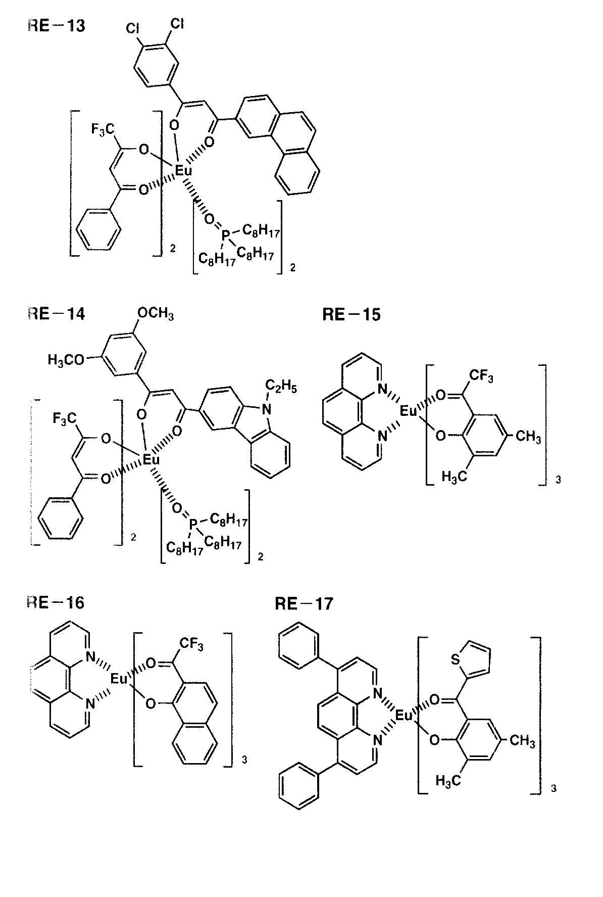
Examples of rare earth complex phosphors used in the present invention include those having, as rare earth metals, Ce, Pr, Nd, Pm, Sm, Eu, Gd, Tb, Dy, Ho, Er, Tm, Yb, etc. The organic ligand that forms can be either aromatic or non-aromatic, and is preferably a compound represented by the following general formula (A).
[0043]
General formula (A) Xa- (Lx)-(Ly) n- (Lz) -Ya
In the formula, Lx, Ly, and Lz each independently represent an atom having two or more bonds, n represents 0 or 1, and Xa represents a substituent having an atom that can be coordinated to the adjacent position of Lx. , Ya represents a substituent having an atom capable of coordinating at a position adjacent to Lz. Further, any part of Xa and Lx may be condensed with each other to form a ring, any part of Ya and Lz may be condensed with each other to form a ring, and Lx and Lz are condensed with each other. Thus, a ring may be formed, and at least one aromatic hydrocarbon ring or aromatic heterocyclic ring exists in the molecule. However, Xa- (Lx)-(Ly) n- (Lz) -Ya is a β-diketone derivative, β-ketoester derivative, β-ketoamide derivative or oxygen atom of the ketone as a sulfur atom or -N (R 201 )-, Crown ether, azacrown ether, thiacrown ether or crown ether with an oxygen atom of any number of sulfur atoms or -N (R 201 ) When the crown ether is replaced with-, there may be no aromatic hydrocarbon ring or aromatic heterocyclic ring. -N (R 201 )-, R 201 Represents a hydrogen atom, an alkyl group, or an aryl group.
[0044]
Where R 201 Each of an alkyl group, an aryl group, and the like represented by general formula (1) and R in general formula (2) 1 ~ R 29 It is synonymous with description in.
[0045]
In the general formula (A), the coordinateable atoms represented by Xa and Ya are specifically an oxygen atom, a nitrogen atom, a sulfur atom, a selenium atom, and a tellurium atom, particularly an oxygen atom, a nitrogen atom, A sulfur atom is preferred.
[0046]
In the general formula (A), the atom having two or more bonds represented by Lx, Ly, and Lz is not particularly limited, but typically, a carbon atom, an oxygen atom, a nitrogen atom, a silicon atom, A titanium atom etc. are mentioned, A carbon atom is preferable.
[0047]
Specific examples of the rare earth complex phosphor represented by the general formula (A) are shown below, but the present invention is not limited thereto.
[0048]
[Chemical 7]
[Chemical 8]
[Chemical 9]
The light emitting layer used in the present invention is formed by forming the above-described preferred material by a known thinning method such as a vacuum deposition method, a spin coating method, an ink jet method, a casting method, or an LB method. Can do. Although the film thickness as a light emitting layer does not have a restriction | limiting in particular, Usually, the range of 5 nm-5 micrometers is preferable. This light emitting layer may have a single layer structure composed of one or two or more of these light emitting materials, or may have a laminated structure composed of a plurality of layers having the same composition or different compositions.
[0052]
In addition, as described in JP-A-57-51781, the light-emitting layer is prepared by dissolving the light-emitting material in a solvent together with a binder such as resin to form a thin film by spin coating or the like. Can be formed. There is no restriction | limiting in particular about the film thickness of the light emitting layer formed in this way, Although it can select suitably according to a condition, Usually, the range of 5 nm-5 micrometers is preferable.
[0053]
The hole transport layer and electron transport layer used in the present invention will be described.
The hole transport layer has a function of transmitting holes injected from the anode to the light emitting layer. By interposing this hole transport layer between the anode and the light emitting layer, a large number of holes can be formed at a lower electric field. Are injected into the light emitting layer, and the electrons injected into the light emitting layer from the cathode, the cathode buffer layer, or the electron transport layer are interfacial in the light emitting layer due to an electron barrier existing at the interface between the light emitting layer and the hole transport layer. In other words, the light emitting efficiency is improved. The material of the hole transport layer (hereinafter referred to as a hole injection material and a hole transport material) is not particularly limited as long as it has the above-mentioned preferable properties. Any material commonly used as an injection transport material or a known material used for a hole transport layer of an EL element can be selected and used.
[0054]
The hole transport material has one of hole injection or transport and electron barrier properties, and may be either organic or inorganic. Examples of the hole transport material include triazole derivatives, oxadiazole derivatives, imidazole derivatives, polyarylalkane derivatives, pyrazoline derivatives and pyrazolone derivatives, phenylenediamine derivatives, arylamine derivatives, amino-substituted chalcone derivatives, oxazole derivatives, styrylanthracene derivatives. Fluorenone derivatives, hydrazone derivatives, stilbene derivatives, silazane derivatives, aniline copolymers, and conductive polymer oligomers, particularly thiophene oligomers. As the hole transport material, those described above can be used, but it is preferable to use a porphyrin compound, an aromatic tertiary amine compound and a styrylamine compound, particularly an aromatic tertiary amine compound.
[0055]
Representative examples of the aromatic tertiary amine compound and styrylamine compound include N, N, N ′, N′-tetraphenyl-4,4′-diaminophenyl; N, N′-diphenyl-N, N ′. -Bis (3-methylphenyl)-[1,1'-biphenyl] -4,4'-diamine (TPD); 2,2-bis (4-di-p-tolylaminophenyl) propane; Bis (4-di-p-tolylaminophenyl) cyclohexane; N, N, N ′, N′-tetra-p-tolyl-4,4′-diaminobiphenyl; 1,1-bis (4-di-p- Tolylaminophenyl) -4-phenylcyclohexane; bis (4-dimethylamino-2-methylphenyl) phenylmethane; bis (4-di-p-tolylaminophenyl) phenylmethane; N, N′-diphenyl-N, N '-Di (4-met Cyphenyl) -4,4′-diaminobiphenyl; N, N, N ′, N′-tetraphenyl-4,4′-diaminodiphenyl ether; 4,4′-bis (diphenylamino) quadriphenyl; N, N, N-tri (p-tolyl) amine; 4- (di-p-tolylamino) -4 ′-[4- (di-p-tolylamino) styryl] stilbene; 4-N, N-diphenylamino- (2-diphenyl) Vinyl) benzene; 3-methoxy-4′-N, N-diphenylaminostilbenzene; N-phenylcarbazole, and further having two condensed aromatic rings described in US Pat. No. 5,061,569 in the molecule For example, 4,4′-bis [N- (1-naphthyl) -N-phenylamino] biphenyl (NPD), triphenylamino described in JP-A-4-308688 4,4 ′, 4 ″ -tris [N- (3-methylphenyl) -N-phenylamino] triphenylamine (MTDATA) in which three units are connected in a starburst type.
[0056]
Furthermore, a polymer material in which these materials are introduced into a polymer chain or these materials are used as a polymer main chain can also be used.
[0057]
In addition, inorganic compounds such as p-type-Si and p-type-SiC can also be used as the hole transport material. The hole transport layer can be formed by thinning the hole hole transport material by a known method such as a vacuum deposition method, a spin coating method, a casting method, or an LB method. Although there is no restriction | limiting in particular about the film thickness of a positive hole transport layer, Usually, it is about 5 nm-5 micrometers. The hole transport layer may have a single layer structure composed of one or more of the above materials, or may have a multilayer structure composed of a plurality of layers having the same composition or different compositions. Furthermore, the electron transport layer used as necessary only has to have a function of transmitting electrons injected from the cathode to the light emitting layer, and the material thereof may be any of conventionally known compounds. You can choose.
[0058]
Examples of materials used for the electron transport layer (hereinafter referred to as electron transport materials) include heterocyclic tetracarboxylic acid anhydrides such as nitro-substituted fluorene derivatives, diphenylquinone derivatives, thiopyran dioxide derivatives, naphthalene perylene, carbodiimides, Examples include fluorenylidenemethane derivatives, anthraquinodimethane and anthrone derivatives, and oxadiazole derivatives. Furthermore, in the above oxadiazole derivative, a thiadiazole derivative in which the oxygen atom of the oxadiazole ring is substituted with a sulfur atom, and a quinoxaline derivative having a quinoxaline ring known as an electron withdrawing group can also be used as an electron transport material.
[0059]
Furthermore, a polymer material in which these materials are introduced into a polymer chain or these materials are used as a polymer main chain can also be used.
[0060]
In addition, metal complexes of 8-quinolinol derivatives such as tris (8-quinolinol) aluminum (Alq), tris (5,7-dichloro-8-quinolinol) aluminum, tris (5,7-dibromo-8-quinolinol) aluminum, Tris (2-methyl-8-quinolinol) aluminum, tris (5-methyl-8-quinolinol) aluminum, bis (8-quinolinol) zinc (Znq), etc., and the central metals of these metal complexes are In, Mg, Cu , Ca, Sn, Ga, or Pb can also be used as an electron transport material.
[0061]
In addition, metal-free or metal phthalocyanine, or those having terminal ends substituted with an alkyl group or a sulfonic acid group can be preferably used as the electron transport material. Further, a distyrylpyrazine derivative used as a material for the light-emitting layer can also be used as an electron transport material. Similarly to the hole transport layer, inorganic semiconductors such as n-type-Si and n-type-SiC can also be used as an electron transport material. Can be used as
[0062]
This electron transport layer can be formed by forming the above compound by a known thinning method such as a vacuum deposition method, a spin coating method, a casting method, or an LB method. Although the film thickness as an electron carrying layer does not have a restriction | limiting in particular, Usually, it selects in 5 nm-5 micrometers. This electron transport layer may have a single layer structure composed of one or two or more of these electron transport materials, or may have a laminated structure composed of a plurality of layers having the same composition or different compositions.
[0063]
Furthermore, a buffer layer (electrode interface layer) may be present between the anode and the light emitting layer or hole injection layer and between the cathode and the light emitting layer or electron injection layer.
[0064]
The buffer layer is a layer that is provided between the electrode and the organic layer in order to lower the driving voltage and improve the light emission efficiency. “The organic EL element and the forefront of its industrialization (issued on November 30, 1998 by NTS Corporation) 2) Chapter 2 “Electrode Materials” (pages 123 to 166) in detail, and includes an anode buffer layer and a cathode buffer layer.
[0065]
The details of the anode buffer layer are described in JP-A-9-45479, 9-260062, and 8-288069. Specific examples thereof include a phthalocyanine buffer layer represented by copper phthalocyanine, and vanadium oxide. And an oxide buffer layer, an amorphous carbon buffer layer, and a polymer buffer layer using a conductive polymer such as polyaniline (emeraldine) or polythiophene.
[0066]
The details of the cathode buffer layer are also described in JP-A-6-325871, JP-A-9-17574, JP-A-10-74586, and the like. Specifically, a metal buffer layer represented by strontium, aluminum and the like, Examples thereof include an alkali metal compound buffer layer typified by lithium fluoride, an alkaline earth metal compound buffer layer typified by magnesium fluoride, and an oxide buffer layer typified by aluminum oxide.
[0067]
In particular, in the organic EL device of the present invention, it is preferable that a cathode buffer layer is present, and a great improvement in luminous efficiency is obtained.
[0068]
The buffer layer is preferably a very thin film, and depending on the material, the film thickness is preferably in the range of 0.1 to 100 nm.
[0069]
Further, in addition to the basic constituent layer, a layer having other functions may be laminated as required. For example, JP-A-11-204258, JP-A-11-204359, and “Organic EL device and its industrialization front line ( It may have a functional layer such as a hole blocking layer described on page 237 of "November 30, 1998, NTS Corporation").
[0070]
In the present invention, at least one polymer of the present invention is present in at least one of the light emitting layer, the hole transport layer, the electron transport layer, the hole blocking layer, the cathode buffer layer, and the anode buffer layer. To do. Preferably, at least one polymer of the present invention is present in the light emitting layer or the hole transport layer.
[0071]
Next, the electrode of the organic EL element will be described. The electrode of the organic EL element consists of a cathode and an anode.
[0072]
As the anode in the organic EL element, an electrode material made of a metal, an alloy, an electrically conductive compound, or a mixture thereof having a high work function (4 eV or more) is preferably used. Specific examples of such electrode materials include metals such as Au, CuI, indium tin oxide (also referred to as ITO: Sn-doped indium oxide), SnO. 2 And conductive transparent materials such as ZnO.
[0073]
The anode may be formed by forming a thin film by depositing these electrode materials by a method such as vapor deposition or sputtering, and a pattern having a desired shape may be formed by a photolithography method, or when the pattern accuracy is not so high (100 μm). As described above, a pattern may be formed through a mask having a desired shape when the electrode material is deposited or sputtered. When light emission is extracted from the anode, it is desirable that the transmittance is greater than 10%, and the sheet resistance as the anode is preferably several hundred Ω / □ or less. Further, although the film thickness depends on the material, it is usually selected in the range of 10 nm to 1 μm, preferably 10 nm to 200 nm.
[0074]
On the other hand, as the cathode, a material having a low work function (4 eV or less) metal (referred to as an electron injecting metal), an alloy, an electrically conductive compound, and a mixture thereof as an electrode material is used. Specific examples of such electrode materials include sodium, sodium-potassium alloy, magnesium, lithium, magnesium / copper mixture, magnesium / silver mixture, magnesium / aluminum mixture, magnesium / indium mixture, aluminum / aluminum oxide (Al 2 O Three ) Mixtures, indium, lithium / aluminum mixtures, rare earth metals and the like. Among these, a mixture of an electron injecting metal and a second metal which is a stable metal having a larger work function value than this from the viewpoint of durability against electron injecting and oxidation, for example, a magnesium / silver mixture, magnesium / Aluminum mixture, magnesium / indium mixture, aluminum / aluminum oxide (Al 2 O Three ) Mixtures, lithium / aluminum mixtures and the like are preferred.
In the present invention, when a cathode buffer layer is provided between the organic compound layer and the cathode, the metal used for the cathode does not necessarily have a low work function, and a metal having a relatively high work function such as aluminum is used. It is also possible to use a non-metallic conductive material such as ITO.
[0075]
The cathode can be produced by forming a thin film of these electrode materials by a method such as vapor deposition or sputtering. Further, the sheet resistance as the cathode is preferably several hundred Ω / □ or less, and the film thickness is usually selected in the range of 10 nm to 1 μm, preferably 50 to 200 nm. In order to transmit light, if either the anode or the cathode of the organic EL element is transparent or translucent, the light emission efficiency is improved, which is convenient.
[0076]
The substrate that is preferably used in the organic EL device of the present invention is not particularly limited in the type such as glass and plastic, and is not particularly limited as long as it is transparent. Examples of the substrate preferably used in the electroluminescent device of the present invention include glass, quartz, and a light transmissive plastic film.
[0077]
Examples of the light transmissive plastic film include polyethylene terephthalate (PET), polyethylene naphthalate (PEN), polyethersulfone (PES), polyetherimide, polyetheretherketone, polyphenylene sulfide, polyarylate, polyimide, and polycarbonate (PC). And a film made of cellulose triacetate (TAC), cellulose acetate propionate (CAP), or the like.
[0078]
Next, a suitable example for producing the organic EL element will be described. As an example, a method for producing an EL device comprising the anode / anode buffer layer / hole transport layer / light emitting layer / electron transport layer / cathode buffer layer / cathode will be described. First, a desired electrode material is formed on a suitable substrate. For example, a thin film made of a material for an anode is formed by a method such as vapor deposition or sputtering so as to have a film thickness of 1 μm or less, preferably in the range of 10 to 200 nm, to produce an anode. Next, a thin film made of materials of an anode buffer layer, a hole transport layer, a light emitting layer, an electron transport layer, and a cathode buffer layer is formed thereon.
As a method for thinning the organic thin film layer, there are a spin coating method, a casting method, a vapor deposition method and the like as described above. From the viewpoint that a homogeneous film is easily obtained and pinholes are not easily generated. Vapor deposition or spin coating is particularly preferred. Further, a different film forming method may be applied for each layer. When a vapor deposition method is employed for film formation, the vapor deposition conditions vary depending on the type of compound used, the target crystal structure of the molecular deposition film, the association structure, etc. -6 -10 -2 It is desirable to select appropriately within the ranges of Pa, vapor deposition rate of 0.01 to 50 nm / second, substrate temperature of −50 to 300 ° C., and film thickness of 5 nm to 5 μm.
[0079]
After forming these layers, a thin film made of a cathode material is formed thereon by a method such as vapor deposition or sputtering so as to have a film thickness of 1 μm or less, preferably in the range of 50 to 200 nm, and a cathode is provided. Thus, a desired EL element can be obtained. The organic EL element is preferably produced from the hole injection layer to the cathode consistently by a single evacuation, but it may be taken out in the middle and subjected to a different film forming method. It is preferable to take into consideration that the operation is performed in a dry inert gas atmosphere.
[0080]
In addition, it is possible to reverse the production order and produce the cathode, the cathode buffer layer, the electron transport layer, the light emitting layer, the hole transport layer, the anode buffer layer, and the anode in this order. When a DC voltage is applied to the EL element thus obtained, light emission can be observed by applying a voltage of about 5 to 40 V with the anode being + and the cathode being-. Further, even when a voltage is applied with the opposite polarity, no current flows and no light emission occurs. Further, when an AC voltage is applied, light is emitted only when the anode is in the + state and the cathode is in the-state. The alternating current waveform to be applied may be arbitrary.
[0081]
The organic EL element of the present invention may be used as a kind of lamp such as an illumination or exposure light source, or a projection device that projects an image, or a display device that directly recognizes a still image or a moving image. (Display) may be used. When used as a display device for reproducing moving images, the driving method may be either a simple matrix (passive matrix) method or an active matrix method. Moreover, it is possible to produce a full-color display device by using 2 or more types of the organic electroluminescent element of this invention which has a different luminescent color. At this time, the organic compound of the present invention used for the light emitting layer is preferably the same. In such a case, there is a high possibility that the materials used for materials other than the light-emitting layer (materials used for the buffer layer, hole transport layer, electron transport layer, etc.) can be made the same. It becomes easy.
[0082]
Furthermore, the organic EL device of the present invention may have a color conversion layer or a color conversion filter containing a fluorescent substance or the like inside or outside the device, and also have a hue improving filter such as a color filter. May be.
[0083]
The organic EL device of the present invention may be used as a kind of lamp for illumination or exposure light source, or may be used as a display device for reproducing still images and moving images. In particular, the drive system when used as a display device for reproducing moving images may be either a simple matrix (passive matrix) system or an active matrix system.
[0084]
【Example】
EXAMPLES Hereinafter, although an Example is given and this invention is demonstrated, this invention is not limited to these.
[0085]
Example 1
<< Preparation of Comparative Organic Electroluminescence Element (OLED-1) >>
After patterning on a substrate (made by NH Techno Glass Co., Ltd .: NA-45) having a 150 nm ITO film on glass as an anode, the transparent support substrate provided with this ITO transparent electrode was ultrasonically cleaned with i-propyl alcohol. Then, it was dried with dry nitrogen gas, and UV ozone cleaning was performed for 5 minutes. 35 mg of poly N-vinylcarbazole (abbreviated as PVCz) and 5 mg of Qd-2 were dissolved in 2 ml of dichloroethane and spin-coated at 3000 rpm for 5 seconds on the washed ITO substrate. After drying, this transparent support substrate was fixed to a substrate holder of a commercially available vacuum deposition apparatus, while 200 mg of bathocuproine (BC) was placed in a molybdenum resistance heating boat and attached to the vacuum deposition apparatus.
[0086]
[Chemical Formula 10]
The vacuum chamber is then 4 × 10 -Four After depressurizing to Pa, the heating boat containing bathocuproine (BC) was energized, heated to 220 ° C., and deposited on a transparent support substrate at a deposition rate of 0.1 to 0.3 nm / sec. An electron transport layer was provided. The substrate temperature during vapor deposition was room temperature.
[0088]
Next, a vacuum chamber is opened, and a stainless steel rectangular perforated mask is placed on the electron injection layer. On the other hand, 3 g of magnesium is placed in a molybdenum resistance heating boat, and 0.02 of silver is placed in a tungsten vapor deposition basket. Put 5g and again vacuum tank 2 × 10 -Four After depressurizing to Pa, power was applied to the magnesium-containing boat to deposit magnesium at a deposition rate of 1.5 to 2.0 nm / sec. At this time, the silver basket was heated at the same time, and the deposition rate was 0.1 nm / sec. The organic EL element OLED-1 for comparison shown in Table 2 was produced by vapor-depositing silver to obtain a cathode made of a mixture of magnesium and silver.
[0089]
<< Production of Comparative Organic Electroluminescence Element (OLED-2) >>
The organic electroluminescence device is the same as the organic electroluminescence device OLED-1, except that the cathode of the OLED-1 is replaced with Al, and a cathode buffer layer is provided by depositing lithium fluoride to a thickness of 0.5 nm between the electron transport layer and the cathode. (OLED-2) was produced.
[0090]
<< Preparation of the organic electroluminescence element (OLED-3 to OLED-11) of the present invention >>
Organic electroluminescent elements (OLED-3 to OLED-6) were produced in the same manner except that poly N-vinylcarbazole in the organic electroluminescent element (OLED-1) was replaced with the polymer shown in Table 2.
[0091]
Further, organic electroluminescence elements (OLED-8 to OLED-11) were produced in the same manner except that the poly N-vinylcarbazole of the organic electroluminescence element (OLED-2) was replaced with the polymer shown in Table 2.
[0092]
These elements were continuously lit by applying a 15 V DC voltage in a dry nitrogen gas atmosphere at 23 ° C., and the light emission luminance (cd / m at the start of lighting) 2 ) And the time to reduce the luminance by half. The light emission luminance is expressed as a relative value when the organic electroluminescence element OLED-1 is 100, and the time when the luminance is halved is expressed as a relative value when the time when the luminance of the organic electroluminescence element OLED-1 is halved is 100. The results are shown in Table 2.
[0093]
[Table 2]
From Table 2, it can be seen that the sample of the present invention is a long-life organic electroluminescence device with improved light emission brightness at the start of lighting and a time when the brightness is reduced by half, compared with comparison, and exhibiting high light emission brightness. it is obvious.
[0095]
It has also been found that introduction of a cathode buffer layer into the organic electroluminescence device of the present invention is effective for obtaining a device with higher luminance and longer life.
[0096]
【The invention's effect】
According to the present invention, an organic electroluminescence device having high emission luminance and a long half-life (long life) can be provided.
Claims (6)
Priority Applications (1)
| Application Number | Priority Date | Filing Date | Title |
|---|---|---|---|
| JP2001184804A JP4457529B2 (en) | 2001-06-19 | 2001-06-19 | Organic electroluminescence device |
Applications Claiming Priority (1)
| Application Number | Priority Date | Filing Date | Title |
|---|---|---|---|
| JP2001184804A JP4457529B2 (en) | 2001-06-19 | 2001-06-19 | Organic electroluminescence device |
Publications (2)
| Publication Number | Publication Date |
|---|---|
| JP2003007466A JP2003007466A (en) | 2003-01-10 |
| JP4457529B2 true JP4457529B2 (en) | 2010-04-28 |
Family
ID=19024505
Family Applications (1)
| Application Number | Title | Priority Date | Filing Date |
|---|---|---|---|
| JP2001184804A Expired - Fee Related JP4457529B2 (en) | 2001-06-19 | 2001-06-19 | Organic electroluminescence device |
Country Status (1)
| Country | Link |
|---|---|
| JP (1) | JP4457529B2 (en) |
Families Citing this family (2)
| Publication number | Priority date | Publication date | Assignee | Title |
|---|---|---|---|---|
| DE102004057086A1 (en) * | 2004-11-25 | 2006-06-08 | Basf Ag | Phenothiazines, -S-oxides and S, S-dioxide and Phenoxazine as an emitter for OLED |
| JP6786858B2 (en) * | 2015-06-19 | 2020-11-18 | 株式会社リコー | Electrochromic compounds and electrochromic compositions |
-
2001
- 2001-06-19 JP JP2001184804A patent/JP4457529B2/en not_active Expired - Fee Related
Also Published As
| Publication number | Publication date |
|---|---|
| JP2003007466A (en) | 2003-01-10 |
Similar Documents
| Publication | Publication Date | Title |
|---|---|---|
| JP4810687B2 (en) | Organic electroluminescence element and display device | |
| JP4103491B2 (en) | Organic electroluminescence element and display device | |
| JP4770033B2 (en) | Organic electroluminescence device | |
| JP3925265B2 (en) | Organic electroluminescence element and display device using the same | |
| JP4103493B2 (en) | Organic electroluminescence element and display device | |
| JP4106974B2 (en) | Organic electroluminescence element and display device | |
| JP4103492B2 (en) | Organic electroluminescence element and display device | |
| JP3969132B2 (en) | Organic electroluminescence element and display device using the same | |
| JP5532020B2 (en) | Organic electroluminescence element and display device using the same | |
| JP2003123983A (en) | Organic electroluminescent element | |
| JP2004031004A (en) | Organic electroluminescence element and display device | |
| JP4048792B2 (en) | Organic electroluminescence element and display device | |
| JP4052024B2 (en) | Organic electroluminescence element and display device | |
| JP4631259B2 (en) | Organic electroluminescence element and display device | |
| JP5202864B2 (en) | Organic electroluminescence element and display device using the same | |
| JP4300788B2 (en) | Organic electroluminescence element and display device | |
| JP3994799B2 (en) | Organic electroluminescence element and display device | |
| JP4442114B2 (en) | Organic electroluminescence element and display device | |
| JP4265216B2 (en) | Organic electroluminescence element and display device | |
| JP4228573B2 (en) | Organic electroluminescence element and display device | |
| JP4656111B2 (en) | Organic electroluminescence device | |
| JP2003064355A (en) | Organic electroluminescence device and full color display device | |
| JP4726384B2 (en) | Organic electroluminescence element and display device | |
| JP4457529B2 (en) | Organic electroluminescence device | |
| JP3997937B2 (en) | Organic electroluminescence element, display device and lighting device |
Legal Events
| Date | Code | Title | Description |
|---|---|---|---|
| A621 | Written request for application examination |
Free format text: JAPANESE INTERMEDIATE CODE: A621 Effective date: 20070214 |
|
| A977 | Report on retrieval |
Free format text: JAPANESE INTERMEDIATE CODE: A971007 Effective date: 20091228 |
|
| TRDD | Decision of grant or rejection written | ||
| A01 | Written decision to grant a patent or to grant a registration (utility model) |
Free format text: JAPANESE INTERMEDIATE CODE: A01 Effective date: 20100119 |
|
| A01 | Written decision to grant a patent or to grant a registration (utility model) |
Free format text: JAPANESE INTERMEDIATE CODE: A01 |
|
| A61 | First payment of annual fees (during grant procedure) |
Free format text: JAPANESE INTERMEDIATE CODE: A61 Effective date: 20100201 |
|
| R150 | Certificate of patent or registration of utility model |
Free format text: JAPANESE INTERMEDIATE CODE: R150 Ref document number: 4457529 Country of ref document: JP Free format text: JAPANESE INTERMEDIATE CODE: R150 |
|
| FPAY | Renewal fee payment (event date is renewal date of database) |
Free format text: PAYMENT UNTIL: 20130219 Year of fee payment: 3 |
|
| FPAY | Renewal fee payment (event date is renewal date of database) |
Free format text: PAYMENT UNTIL: 20130219 Year of fee payment: 3 |
|
| FPAY | Renewal fee payment (event date is renewal date of database) |
Free format text: PAYMENT UNTIL: 20140219 Year of fee payment: 4 |
|
| S531 | Written request for registration of change of domicile |
Free format text: JAPANESE INTERMEDIATE CODE: R313531 |
|
| S533 | Written request for registration of change of name |
Free format text: JAPANESE INTERMEDIATE CODE: R313533 |
|
| R350 | Written notification of registration of transfer |
Free format text: JAPANESE INTERMEDIATE CODE: R350 |
|
| LAPS | Cancellation because of no payment of annual fees |