JP4518113B2 - 電子部品内蔵基板及びその製造方法 - Google Patents
電子部品内蔵基板及びその製造方法 Download PDFInfo
- Publication number
- JP4518113B2 JP4518113B2 JP2007193836A JP2007193836A JP4518113B2 JP 4518113 B2 JP4518113 B2 JP 4518113B2 JP 2007193836 A JP2007193836 A JP 2007193836A JP 2007193836 A JP2007193836 A JP 2007193836A JP 4518113 B2 JP4518113 B2 JP 4518113B2
- Authority
- JP
- Japan
- Prior art keywords
- electronic component
- substrate
- thermal expansion
- linear thermal
- insulating layer
- Prior art date
- Legal status (The legal status is an assumption and is not a legal conclusion. Google has not performed a legal analysis and makes no representation as to the accuracy of the status listed.)
- Active
Links
Images
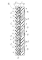


Classifications
-
- H—ELECTRICITY
- H05—ELECTRIC TECHNIQUES NOT OTHERWISE PROVIDED FOR
- H05K—PRINTED CIRCUITS; CASINGS OR CONSTRUCTIONAL DETAILS OF ELECTRIC APPARATUS; MANUFACTURE OF ASSEMBLAGES OF ELECTRICAL COMPONENTS
- H05K1/00—Printed circuits
- H05K1/18—Printed circuits structurally associated with non-printed electric components
- H05K1/182—Printed circuits structurally associated with non-printed electric components associated with components mounted in printed circuit boards [PCB], e.g. insert-mounted components [IMC]
- H05K1/185—Printed circuits structurally associated with non-printed electric components associated with components mounted in printed circuit boards [PCB], e.g. insert-mounted components [IMC] associated with components encapsulated in the insulating substrate of the PCBs; associated with components incorporated in internal layers of multilayer circuit boards
-
- H—ELECTRICITY
- H05—ELECTRIC TECHNIQUES NOT OTHERWISE PROVIDED FOR
- H05K—PRINTED CIRCUITS; CASINGS OR CONSTRUCTIONAL DETAILS OF ELECTRIC APPARATUS; MANUFACTURE OF ASSEMBLAGES OF ELECTRICAL COMPONENTS
- H05K1/00—Printed circuits
- H05K1/02—Details
- H05K1/0271—Arrangements for reducing stress or warp in rigid printed circuit boards, e.g. caused by loads, vibrations or differences in thermal expansion
-
- H—ELECTRICITY
- H05—ELECTRIC TECHNIQUES NOT OTHERWISE PROVIDED FOR
- H05K—PRINTED CIRCUITS; CASINGS OR CONSTRUCTIONAL DETAILS OF ELECTRIC APPARATUS; MANUFACTURE OF ASSEMBLAGES OF ELECTRICAL COMPONENTS
- H05K3/00—Apparatus or processes for manufacturing printed circuits
- H05K3/0097—Processing two or more printed circuits simultaneously, e.g. made from a common substrate, or temporarily stacked circuit boards
-
- H—ELECTRICITY
- H10—SEMICONDUCTOR DEVICES; ELECTRIC SOLID-STATE DEVICES NOT OTHERWISE PROVIDED FOR
- H10W—GENERIC PACKAGES, INTERCONNECTIONS, CONNECTORS OR OTHER CONSTRUCTIONAL DETAILS OF DEVICES COVERED BY CLASS H10
- H10W70/00—Package substrates; Interposers; Redistribution layers [RDL]
- H10W70/01—Manufacture or treatment
- H10W70/05—Manufacture or treatment of insulating or insulated package substrates, or of interposers, or of redistribution layers
- H10W70/08—Manufacture or treatment of insulating or insulated package substrates, or of interposers, or of redistribution layers by depositing layers on the chip or wafer, e.g. "chip-first" RDLs
- H10W70/09—Manufacture or treatment of insulating or insulated package substrates, or of interposers, or of redistribution layers by depositing layers on the chip or wafer, e.g. "chip-first" RDLs extending onto an encapsulation that laterally surrounds the chip or wafer, e.g. fan-out wafer level package [FOWLP] RDLs
-
- H—ELECTRICITY
- H10—SEMICONDUCTOR DEVICES; ELECTRIC SOLID-STATE DEVICES NOT OTHERWISE PROVIDED FOR
- H10W—GENERIC PACKAGES, INTERCONNECTIONS, CONNECTORS OR OTHER CONSTRUCTIONAL DETAILS OF DEVICES COVERED BY CLASS H10
- H10W70/00—Package substrates; Interposers; Redistribution layers [RDL]
- H10W70/01—Manufacture or treatment
- H10W70/05—Manufacture or treatment of insulating or insulated package substrates, or of interposers, or of redistribution layers
- H10W70/093—Connecting or disconnecting other interconnections thereto or therefrom, e.g. connecting bond wires or bumps
-
- H—ELECTRICITY
- H10—SEMICONDUCTOR DEVICES; ELECTRIC SOLID-STATE DEVICES NOT OTHERWISE PROVIDED FOR
- H10W—GENERIC PACKAGES, INTERCONNECTIONS, CONNECTORS OR OTHER CONSTRUCTIONAL DETAILS OF DEVICES COVERED BY CLASS H10
- H10W70/00—Package substrates; Interposers; Redistribution layers [RDL]
- H10W70/60—Insulating or insulated package substrates; Interposers; Redistribution layers
- H10W70/611—Insulating or insulated package substrates; Interposers; Redistribution layers for connecting multiple chips together
- H10W70/614—Insulating or insulated package substrates; Interposers; Redistribution layers for connecting multiple chips together the multiple chips being integrally enclosed
-
- H—ELECTRICITY
- H10—SEMICONDUCTOR DEVICES; ELECTRIC SOLID-STATE DEVICES NOT OTHERWISE PROVIDED FOR
- H10W—GENERIC PACKAGES, INTERCONNECTIONS, CONNECTORS OR OTHER CONSTRUCTIONAL DETAILS OF DEVICES COVERED BY CLASS H10
- H10W90/00—Package configurations
-
- H—ELECTRICITY
- H05—ELECTRIC TECHNIQUES NOT OTHERWISE PROVIDED FOR
- H05K—PRINTED CIRCUITS; CASINGS OR CONSTRUCTIONAL DETAILS OF ELECTRIC APPARATUS; MANUFACTURE OF ASSEMBLAGES OF ELECTRICAL COMPONENTS
- H05K2201/00—Indexing scheme relating to printed circuits covered by H05K1/00
- H05K2201/06—Thermal details
- H05K2201/068—Thermal details wherein the coefficient of thermal expansion is important
-
- H—ELECTRICITY
- H05—ELECTRIC TECHNIQUES NOT OTHERWISE PROVIDED FOR
- H05K—PRINTED CIRCUITS; CASINGS OR CONSTRUCTIONAL DETAILS OF ELECTRIC APPARATUS; MANUFACTURE OF ASSEMBLAGES OF ELECTRICAL COMPONENTS
- H05K2201/00—Indexing scheme relating to printed circuits covered by H05K1/00
- H05K2201/20—Details of printed circuits not provided for in H05K2201/01 - H05K2201/10
- H05K2201/2009—Reinforced areas, e.g. for a specific part of a flexible printed circuit
-
- H—ELECTRICITY
- H05—ELECTRIC TECHNIQUES NOT OTHERWISE PROVIDED FOR
- H05K—PRINTED CIRCUITS; CASINGS OR CONSTRUCTIONAL DETAILS OF ELECTRIC APPARATUS; MANUFACTURE OF ASSEMBLAGES OF ELECTRICAL COMPONENTS
- H05K2203/00—Indexing scheme relating to apparatus or processes for manufacturing printed circuits covered by H05K3/00
- H05K2203/01—Tools for processing; Objects used during processing
- H05K2203/0147—Carriers and holders
- H05K2203/0169—Using a temporary frame during processing
-
- H—ELECTRICITY
- H05—ELECTRIC TECHNIQUES NOT OTHERWISE PROVIDED FOR
- H05K—PRINTED CIRCUITS; CASINGS OR CONSTRUCTIONAL DETAILS OF ELECTRIC APPARATUS; MANUFACTURE OF ASSEMBLAGES OF ELECTRICAL COMPONENTS
- H05K3/00—Apparatus or processes for manufacturing printed circuits
- H05K3/0011—Working of insulating substrates or insulating layers
- H05K3/0044—Mechanical working of the substrate, e.g. drilling or punching
- H05K3/0052—Depaneling, i.e. dividing a panel into circuit boards; Working of the edges of circuit boards
-
- H—ELECTRICITY
- H05—ELECTRIC TECHNIQUES NOT OTHERWISE PROVIDED FOR
- H05K—PRINTED CIRCUITS; CASINGS OR CONSTRUCTIONAL DETAILS OF ELECTRIC APPARATUS; MANUFACTURE OF ASSEMBLAGES OF ELECTRICAL COMPONENTS
- H05K3/00—Apparatus or processes for manufacturing printed circuits
- H05K3/46—Manufacturing multilayer circuits
- H05K3/4602—Manufacturing multilayer circuits characterized by a special circuit board as base or central core whereon additional circuit layers are built or additional circuit boards are laminated
-
- H—ELECTRICITY
- H10—SEMICONDUCTOR DEVICES; ELECTRIC SOLID-STATE DEVICES NOT OTHERWISE PROVIDED FOR
- H10W—GENERIC PACKAGES, INTERCONNECTIONS, CONNECTORS OR OTHER CONSTRUCTIONAL DETAILS OF DEVICES COVERED BY CLASS H10
- H10W70/00—Package substrates; Interposers; Redistribution layers [RDL]
- H10W70/099—Connecting interconnections to insulating or insulated package substrates, interposers or redistribution layers
-
- H—ELECTRICITY
- H10—SEMICONDUCTOR DEVICES; ELECTRIC SOLID-STATE DEVICES NOT OTHERWISE PROVIDED FOR
- H10W—GENERIC PACKAGES, INTERCONNECTIONS, CONNECTORS OR OTHER CONSTRUCTIONAL DETAILS OF DEVICES COVERED BY CLASS H10
- H10W70/00—Package substrates; Interposers; Redistribution layers [RDL]
- H10W70/60—Insulating or insulated package substrates; Interposers; Redistribution layers
-
- H—ELECTRICITY
- H10—SEMICONDUCTOR DEVICES; ELECTRIC SOLID-STATE DEVICES NOT OTHERWISE PROVIDED FOR
- H10W—GENERIC PACKAGES, INTERCONNECTIONS, CONNECTORS OR OTHER CONSTRUCTIONAL DETAILS OF DEVICES COVERED BY CLASS H10
- H10W72/00—Interconnections or connectors in packages
- H10W72/01—Manufacture or treatment
- H10W72/0198—Manufacture or treatment batch processes
-
- H—ELECTRICITY
- H10—SEMICONDUCTOR DEVICES; ELECTRIC SOLID-STATE DEVICES NOT OTHERWISE PROVIDED FOR
- H10W—GENERIC PACKAGES, INTERCONNECTIONS, CONNECTORS OR OTHER CONSTRUCTIONAL DETAILS OF DEVICES COVERED BY CLASS H10
- H10W72/00—Interconnections or connectors in packages
- H10W72/071—Connecting or disconnecting
- H10W72/073—Connecting or disconnecting of die-attach connectors
-
- H—ELECTRICITY
- H10—SEMICONDUCTOR DEVICES; ELECTRIC SOLID-STATE DEVICES NOT OTHERWISE PROVIDED FOR
- H10W—GENERIC PACKAGES, INTERCONNECTIONS, CONNECTORS OR OTHER CONSTRUCTIONAL DETAILS OF DEVICES COVERED BY CLASS H10
- H10W72/00—Interconnections or connectors in packages
- H10W72/851—Dispositions of multiple connectors or interconnections
- H10W72/874—On different surfaces
-
- H—ELECTRICITY
- H10—SEMICONDUCTOR DEVICES; ELECTRIC SOLID-STATE DEVICES NOT OTHERWISE PROVIDED FOR
- H10W—GENERIC PACKAGES, INTERCONNECTIONS, CONNECTORS OR OTHER CONSTRUCTIONAL DETAILS OF DEVICES COVERED BY CLASS H10
- H10W72/00—Interconnections or connectors in packages
- H10W72/90—Bond pads, in general
- H10W72/941—Dispositions of bond pads
- H10W72/9413—Dispositions of bond pads on encapsulations
-
- H—ELECTRICITY
- H10—SEMICONDUCTOR DEVICES; ELECTRIC SOLID-STATE DEVICES NOT OTHERWISE PROVIDED FOR
- H10W—GENERIC PACKAGES, INTERCONNECTIONS, CONNECTORS OR OTHER CONSTRUCTIONAL DETAILS OF DEVICES COVERED BY CLASS H10
- H10W90/00—Package configurations
- H10W90/701—Package configurations characterised by the relative positions of pads or connectors relative to package parts
- H10W90/721—Package configurations characterised by the relative positions of pads or connectors relative to package parts of bump connectors
- H10W90/724—Package configurations characterised by the relative positions of pads or connectors relative to package parts of bump connectors between a chip and a stacked insulating package substrate, interposer or RDL
-
- Y—GENERAL TAGGING OF NEW TECHNOLOGICAL DEVELOPMENTS; GENERAL TAGGING OF CROSS-SECTIONAL TECHNOLOGIES SPANNING OVER SEVERAL SECTIONS OF THE IPC; TECHNICAL SUBJECTS COVERED BY FORMER USPC CROSS-REFERENCE ART COLLECTIONS [XRACs] AND DIGESTS
- Y10—TECHNICAL SUBJECTS COVERED BY FORMER USPC
- Y10T—TECHNICAL SUBJECTS COVERED BY FORMER US CLASSIFICATION
- Y10T29/00—Metal working
- Y10T29/49—Method of mechanical manufacture
- Y10T29/49002—Electrical device making
- Y10T29/49117—Conductor or circuit manufacturing
- Y10T29/49124—On flat or curved insulated base, e.g., printed circuit, etc.
- Y10T29/4913—Assembling to base an electrical component, e.g., capacitor, etc.
- Y10T29/49146—Assembling to base an electrical component, e.g., capacitor, etc. with encapsulating, e.g., potting, etc.
Landscapes
- Engineering & Computer Science (AREA)
- Microelectronics & Electronic Packaging (AREA)
- Manufacturing & Machinery (AREA)
- Production Of Multi-Layered Print Wiring Board (AREA)
- Structure Of Printed Boards (AREA)
- Structures For Mounting Electric Components On Printed Circuit Boards (AREA)
Priority Applications (5)
| Application Number | Priority Date | Filing Date | Title |
|---|---|---|---|
| JP2007193836A JP4518113B2 (ja) | 2007-07-25 | 2007-07-25 | 電子部品内蔵基板及びその製造方法 |
| US12/219,355 US8237059B2 (en) | 2007-07-25 | 2008-07-21 | Electronic component-embedded board and method of manufacturing the same |
| EP08013361A EP2019571B1 (fr) | 2007-07-25 | 2008-07-24 | Carte imprimée comprenant un composant électronique enterré et son procédé de fabrication |
| CN2008101442136A CN101355858B (zh) | 2007-07-25 | 2008-07-25 | 电子部件内置基板及其制造方法 |
| US13/533,176 US20120285013A1 (en) | 2007-07-25 | 2012-06-26 | Electronic Component-Embedded Board and Method of Manufacturing the Same |
Applications Claiming Priority (1)
| Application Number | Priority Date | Filing Date | Title |
|---|---|---|---|
| JP2007193836A JP4518113B2 (ja) | 2007-07-25 | 2007-07-25 | 電子部品内蔵基板及びその製造方法 |
Publications (2)
| Publication Number | Publication Date |
|---|---|
| JP2009032823A JP2009032823A (ja) | 2009-02-12 |
| JP4518113B2 true JP4518113B2 (ja) | 2010-08-04 |
Family
ID=40011038
Family Applications (1)
| Application Number | Title | Priority Date | Filing Date |
|---|---|---|---|
| JP2007193836A Active JP4518113B2 (ja) | 2007-07-25 | 2007-07-25 | 電子部品内蔵基板及びその製造方法 |
Country Status (4)
| Country | Link |
|---|---|
| US (2) | US8237059B2 (fr) |
| EP (1) | EP2019571B1 (fr) |
| JP (1) | JP4518113B2 (fr) |
| CN (1) | CN101355858B (fr) |
Families Citing this family (17)
| Publication number | Priority date | Publication date | Assignee | Title |
|---|---|---|---|---|
| JP4518113B2 (ja) * | 2007-07-25 | 2010-08-04 | Tdk株式会社 | 電子部品内蔵基板及びその製造方法 |
| US8921705B2 (en) * | 2008-11-28 | 2014-12-30 | Ibiden Co., Ltd. | Wiring board and fabrication method therefor |
| US8945329B2 (en) * | 2011-06-24 | 2015-02-03 | Ibiden Co., Ltd. | Printed wiring board and method for manufacturing printed wiring board |
| JP2015018979A (ja) * | 2013-07-12 | 2015-01-29 | イビデン株式会社 | プリント配線板 |
| KR102250997B1 (ko) | 2014-05-02 | 2021-05-12 | 삼성전자주식회사 | 반도체 패키지 |
| KR101969730B1 (ko) * | 2014-12-19 | 2019-04-17 | 후지필름 가부시키가이샤 | 다층 배선 기판 |
| KR101602377B1 (ko) | 2015-08-13 | 2016-03-15 | 주식회사 이오비스 | 3차원 형상 측정 방법 |
| DE102016212129B4 (de) * | 2016-07-04 | 2022-05-19 | Schweizer Electronic Ag | Hochfrequenz-Sende-/Empfangselement und Verfahren zur Herstellung eines Hochfrequenz-Sende-/Empfangselementes |
| TWI645973B (zh) | 2017-12-15 | 2019-01-01 | 律勝科技股份有限公司 | 聚醯亞胺薄化軟性基板及其製造方法 |
| WO2020067320A1 (fr) * | 2018-09-27 | 2020-04-02 | 株式会社村田製作所 | Substrat multicouche en résine |
| CN111511104B (zh) * | 2019-01-31 | 2024-05-28 | 奥特斯奥地利科技与系统技术有限公司 | 部件承载件以及制造部件承载件的方法 |
| US11277917B2 (en) | 2019-03-12 | 2022-03-15 | Advanced Semiconductor Engineering, Inc. | Embedded component package structure, embedded type panel substrate and manufacturing method thereof |
| JP7380681B2 (ja) * | 2019-04-26 | 2023-11-15 | Tdk株式会社 | 集合基板及びその製造方法 |
| US11296030B2 (en) | 2019-04-29 | 2022-04-05 | Advanced Semiconductor Engineering, Inc. | Embedded component package structure and manufacturing method thereof |
| US10950551B2 (en) | 2019-04-29 | 2021-03-16 | Advanced Semiconductor Engineering, Inc. | Embedded component package structure and manufacturing method thereof |
| US11778752B2 (en) * | 2020-01-21 | 2023-10-03 | Avary Holding (Shenzhen) Co., Limited. | Circuit board with embedded electronic component and method for manufacturing the same |
| US11848280B2 (en) * | 2020-11-25 | 2023-12-19 | ADVANCED SEMlCONDUCTOR ENGINEERING, INC. | Method for manufacturing assembly structure by using frame structure on substrate |
Family Cites Families (24)
| Publication number | Priority date | Publication date | Assignee | Title |
|---|---|---|---|---|
| JPH0770645B2 (ja) | 1986-06-11 | 1995-07-31 | 日本電気株式会社 | 混成集積回路 |
| US5233222A (en) * | 1992-07-27 | 1993-08-03 | Motorola, Inc. | Semiconductor device having window-frame flag with tapered edge in opening |
| JP3447029B2 (ja) | 1995-11-07 | 2003-09-16 | イビデン株式会社 | プリント配線板製造方法 |
| US5844319A (en) * | 1997-03-03 | 1998-12-01 | Motorola Corporation | Microelectronic assembly with collar surrounding integrated circuit component on a substrate |
| JP3921756B2 (ja) * | 1997-10-06 | 2007-05-30 | 株式会社デンソー | プリント基板およびその製造方法 |
| WO2000063970A1 (fr) | 1999-04-16 | 2000-10-26 | Matsushita Electric Industrial Co., Ltd. | Composant modulaire et son procede de production |
| JP3619395B2 (ja) * | 1999-07-30 | 2005-02-09 | 京セラ株式会社 | 半導体素子内蔵配線基板およびその製造方法 |
| DE60039547D1 (de) * | 1999-09-27 | 2008-08-28 | Matsushita Electric Industrial Co Ltd | Bestückungsverfahren und Bestückungsvorrichtung |
| JP2001284783A (ja) * | 2000-03-30 | 2001-10-12 | Shinko Electric Ind Co Ltd | 表面実装用基板及び表面実装構造 |
| JP2002016173A (ja) * | 2000-06-30 | 2002-01-18 | Mitsubishi Electric Corp | 半導体装置 |
| JP3816380B2 (ja) | 2001-12-14 | 2006-08-30 | 富士通株式会社 | 吸熱用ダミー部品を備えた基板ユニット及びその製造方法 |
| JP4026705B2 (ja) * | 2002-05-27 | 2007-12-26 | Tdk株式会社 | 積層型電子部品を構成する層及び積層型電子部品の製造方法 |
| JP2003347741A (ja) * | 2002-05-30 | 2003-12-05 | Taiyo Yuden Co Ltd | 複合多層基板およびそれを用いたモジュール |
| JP2004071698A (ja) * | 2002-08-02 | 2004-03-04 | Hitachi Metals Ltd | 半導体パッケージ |
| JP3951854B2 (ja) * | 2002-08-09 | 2007-08-01 | カシオ計算機株式会社 | 半導体装置およびその製造方法 |
| US7394663B2 (en) * | 2003-02-18 | 2008-07-01 | Matsushita Electric Industrial Co., Ltd. | Electronic component built-in module and method of manufacturing the same |
| JP4194408B2 (ja) * | 2003-04-03 | 2008-12-10 | 日本特殊陶業株式会社 | 補強材付き基板、半導体素子と補強材と基板とからなる配線基板 |
| JP4135565B2 (ja) * | 2003-06-06 | 2008-08-20 | 松下電器産業株式会社 | 電子回路装置およびその製造方法 |
| JP2005167141A (ja) | 2003-12-05 | 2005-06-23 | Ibiden Co Ltd | プリント配線板の製造方法及び多層プリント配線板 |
| JP2005251792A (ja) * | 2004-03-01 | 2005-09-15 | Fujitsu Ltd | 配線基板およびその製造方法 |
| JP3914239B2 (ja) * | 2005-03-15 | 2007-05-16 | 新光電気工業株式会社 | 配線基板および配線基板の製造方法 |
| JP4526983B2 (ja) * | 2005-03-15 | 2010-08-18 | 新光電気工業株式会社 | 配線基板の製造方法 |
| US8829661B2 (en) * | 2006-03-10 | 2014-09-09 | Freescale Semiconductor, Inc. | Warp compensated package and method |
| JP4518113B2 (ja) * | 2007-07-25 | 2010-08-04 | Tdk株式会社 | 電子部品内蔵基板及びその製造方法 |
-
2007
- 2007-07-25 JP JP2007193836A patent/JP4518113B2/ja active Active
-
2008
- 2008-07-21 US US12/219,355 patent/US8237059B2/en active Active
- 2008-07-24 EP EP08013361A patent/EP2019571B1/fr active Active
- 2008-07-25 CN CN2008101442136A patent/CN101355858B/zh active Active
-
2012
- 2012-06-26 US US13/533,176 patent/US20120285013A1/en not_active Abandoned
Also Published As
| Publication number | Publication date |
|---|---|
| US20090025971A1 (en) | 2009-01-29 |
| US20120285013A1 (en) | 2012-11-15 |
| JP2009032823A (ja) | 2009-02-12 |
| EP2019571A2 (fr) | 2009-01-28 |
| CN101355858B (zh) | 2011-04-06 |
| US8237059B2 (en) | 2012-08-07 |
| EP2019571B1 (fr) | 2012-09-05 |
| EP2019571A3 (fr) | 2010-04-14 |
| CN101355858A (zh) | 2009-01-28 |
Similar Documents
| Publication | Publication Date | Title |
|---|---|---|
| JP4518113B2 (ja) | 電子部品内蔵基板及びその製造方法 | |
| JP4518114B2 (ja) | 電子部品内蔵基板及びその製造方法 | |
| JP4487271B2 (ja) | 集合基板及びその製造方法 | |
| CN1269199C (zh) | 倒装片型半导体器件及其制造方法 | |
| JP5540276B2 (ja) | 電子部品内蔵基板及びその製造方法 | |
| JP3945483B2 (ja) | 半導体装置の製造方法 | |
| CN106328607B (zh) | 半导体器件及其制造方法 | |
| JP5441007B2 (ja) | 電子部品内蔵基板の製造方法 | |
| US20120292778A1 (en) | Embedded semiconductor power modules and packages | |
| CN105304580B (zh) | 半导体装置及其制造方法 | |
| CN1254860C (zh) | 电路装置的制造方法 | |
| JP2011151048A (ja) | 電子部品の製造方法および電子部品 | |
| JP2005123493A (ja) | 配線基板及び素子実装基板 | |
| JP5013138B2 (ja) | 集合基板及びその製造方法 | |
| JP5097006B2 (ja) | プリント配線基板及びその製造方法 | |
| JP5098313B2 (ja) | 配線基板 | |
| JP2005191157A (ja) | 半導体装置およびその製造方法 | |
| JP4209341B2 (ja) | 半導体装置およびその製造方法 | |
| JP2013062424A (ja) | 半導体装置の製造方法およびその方法により製造された半導体装置 | |
| JP2008021944A (ja) | 多層配線基板及びその製造方法 |
Legal Events
| Date | Code | Title | Description |
|---|---|---|---|
| A621 | Written request for application examination |
Free format text: JAPANESE INTERMEDIATE CODE: A621 Effective date: 20090324 |
|
| A977 | Report on retrieval |
Free format text: JAPANESE INTERMEDIATE CODE: A971007 Effective date: 20090716 |
|
| A131 | Notification of reasons for refusal |
Free format text: JAPANESE INTERMEDIATE CODE: A131 Effective date: 20090721 |
|
| A521 | Request for written amendment filed |
Free format text: JAPANESE INTERMEDIATE CODE: A523 Effective date: 20090915 |
|
| A131 | Notification of reasons for refusal |
Free format text: JAPANESE INTERMEDIATE CODE: A131 Effective date: 20100305 |
|
| A521 | Request for written amendment filed |
Free format text: JAPANESE INTERMEDIATE CODE: A523 Effective date: 20100408 |
|
| TRDD | Decision of grant or rejection written | ||
| A01 | Written decision to grant a patent or to grant a registration (utility model) |
Free format text: JAPANESE INTERMEDIATE CODE: A01 Effective date: 20100427 |
|
| A01 | Written decision to grant a patent or to grant a registration (utility model) |
Free format text: JAPANESE INTERMEDIATE CODE: A01 |
|
| A61 | First payment of annual fees (during grant procedure) |
Free format text: JAPANESE INTERMEDIATE CODE: A61 Effective date: 20100510 |
|
| FPAY | Renewal fee payment (event date is renewal date of database) |
Free format text: PAYMENT UNTIL: 20130528 Year of fee payment: 3 |
|
| R150 | Certificate of patent or registration of utility model |
Free format text: JAPANESE INTERMEDIATE CODE: R150 Ref document number: 4518113 Country of ref document: JP |
|
| FPAY | Renewal fee payment (event date is renewal date of database) |
Free format text: PAYMENT UNTIL: 20140528 Year of fee payment: 4 |
|
| R250 | Receipt of annual fees |
Free format text: JAPANESE INTERMEDIATE CODE: R250 |
|
| R250 | Receipt of annual fees |
Free format text: JAPANESE INTERMEDIATE CODE: R250 |