JP4535367B2 - 集積回路装置 - Google Patents
集積回路装置 Download PDFInfo
- Publication number
- JP4535367B2 JP4535367B2 JP2004153456A JP2004153456A JP4535367B2 JP 4535367 B2 JP4535367 B2 JP 4535367B2 JP 2004153456 A JP2004153456 A JP 2004153456A JP 2004153456 A JP2004153456 A JP 2004153456A JP 4535367 B2 JP4535367 B2 JP 4535367B2
- Authority
- JP
- Japan
- Prior art keywords
- integrated circuit
- temperature
- circuit device
- temperature monitoring
- sensor member
- Prior art date
- Legal status (The legal status is an assumption and is not a legal conclusion. Google has not performed a legal analysis and makes no representation as to the accuracy of the status listed.)
- Expired - Fee Related
Links
Images


Classifications
-
- H—ELECTRICITY
- H10—SEMICONDUCTOR DEVICES; ELECTRIC SOLID-STATE DEVICES NOT OTHERWISE PROVIDED FOR
- H10D—INORGANIC ELECTRIC SEMICONDUCTOR DEVICES
- H10D84/00—Integrated devices formed in or on semiconductor substrates that comprise only semiconducting layers, e.g. on Si wafers or on GaAs-on-Si wafers
- H10D84/80—Integrated devices formed in or on semiconductor substrates that comprise only semiconducting layers, e.g. on Si wafers or on GaAs-on-Si wafers characterised by the integration of at least one component covered by groups H10D12/00 or H10D30/00, e.g. integration of IGFETs
- H10D84/811—Combinations of field-effect devices and one or more diodes, capacitors or resistors
-
- G—PHYSICS
- G01—MEASURING; TESTING
- G01J—MEASUREMENT OF INTENSITY, VELOCITY, SPECTRAL CONTENT, POLARISATION, PHASE OR PULSE CHARACTERISTICS OF INFRARED, VISIBLE OR ULTRAVIOLET LIGHT; COLORIMETRY; RADIATION PYROMETRY
- G01J5/00—Radiation pyrometry, e.g. infrared or optical thermometry
- G01J5/10—Radiation pyrometry, e.g. infrared or optical thermometry using electric radiation detectors
- G01J5/20—Radiation pyrometry, e.g. infrared or optical thermometry using electric radiation detectors using resistors, thermistors or semiconductors sensitive to radiation, e.g. photoconductive devices
- G01J5/22—Electrical features thereof
- G01J5/24—Use of specially adapted circuits, e.g. bridge circuits
-
- H—ELECTRICITY
- H10—SEMICONDUCTOR DEVICES; ELECTRIC SOLID-STATE DEVICES NOT OTHERWISE PROVIDED FOR
- H10D—INORGANIC ELECTRIC SEMICONDUCTOR DEVICES
- H10D84/00—Integrated devices formed in or on semiconductor substrates that comprise only semiconducting layers, e.g. on Si wafers or on GaAs-on-Si wafers
- H10D84/80—Integrated devices formed in or on semiconductor substrates that comprise only semiconducting layers, e.g. on Si wafers or on GaAs-on-Si wafers characterised by the integration of at least one component covered by groups H10D12/00 or H10D30/00, e.g. integration of IGFETs
- H10D84/811—Combinations of field-effect devices and one or more diodes, capacitors or resistors
- H10D84/817—Combinations of field-effect devices and resistors only
-
- H—ELECTRICITY
- H10—SEMICONDUCTOR DEVICES; ELECTRIC SOLID-STATE DEVICES NOT OTHERWISE PROVIDED FOR
- H10D—INORGANIC ELECTRIC SEMICONDUCTOR DEVICES
- H10D89/00—Aspects of integrated devices not covered by groups H10D84/00 - H10D88/00
- H10D89/60—Integrated devices comprising arrangements for electrical or thermal protection, e.g. protection circuits against electrostatic discharge [ESD]
Landscapes
- Physics & Mathematics (AREA)
- General Physics & Mathematics (AREA)
- Spectroscopy & Molecular Physics (AREA)
- Semiconductor Integrated Circuits (AREA)
- Metal-Oxide And Bipolar Metal-Oxide Semiconductor Integrated Circuits (AREA)
- Photometry And Measurement Of Optical Pulse Characteristics (AREA)
Description
本発明に係る集積回路装置において、前記集積回路装置の外部の温度変化により、前記センサ部材の抵抗値が変化してもよく、前記集積回路装置自体の温度変化により、前記センサ部材の抵抗値が変化してもよい。これにより、前記センサ部材の電気抵抗値を検出することにより、集積回路装置の温度を測定することができ、前記センサ部材を温度センサとして使用することができる。
また、本発明に係る集積回路装置において、前記センサ部材が前記多層配線層上に設けられていることが好ましい。これにより、センサ部材を形成する酸化バナジウムが基板及び多層配線層を汚染することがなく、基板及び多層配線層を製造する製造装置を汚染することもない。
センサ部材の断面に流れる電流の最大電流密度:100μA/μm 2 以下
図4は横軸にセンサ部材(温度モニタ部材)の電流方向の長さをとり、縦軸にセンサ部材の断面に流れる幅1μm当たりの電流値及び電流密度の測定結果をとって、センサ部材の形状と電流の大きさとの関係を示すグラフ図である。図4に示す測定においては、センサ部材を酸化バナジウム膜により形成し、この酸化バナジウム膜の幅を5μm、10μm、50μmの3水準とし、酸化バナジウム膜の膜厚を0.1μmとし、センサ部材の両端に印加する電圧を1Vとしている。そして、図4においては、電流を流すことによるセンサ部材(酸化バナジウム膜)の破壊の有無を表記している。

次に、本発明の参考形態について説明する。図5は本参考形態に係る集積回路装置を示す断面図である。本参考形態に係る集積回路装置は、シリコン基板上に複数個の赤外線センサがマトリクス状に配列された熱型赤外線検出器である。この熱型赤外線検出器は、赤外線カメラの受光部に搭載されている。
図5に示すように、本参考形態に係る熱型赤外線検出器31においては、シリコン基板32が設けられており、このシリコン基板32の表面に複数の赤外線センサ33がマトリクス状に配列されており、各赤外線センサ33が各画素を構成している。各赤外線センサ33においては、導電材料からなる1対の梁34が、シリコン基板32から立設している。即ち、梁34の根元部は、シリコン基板32に固定されている。そして、1対の梁34は制御回路(図示せず)に接続されており、この制御回路により電源電位Vcc及び接地電位GNDが夫々印加されるようになっている。また、梁34の先端部はシリコン基板32から離隔しており、この先端部間において、赤外線センサ部材35が支持されている。
次に、本参考形態の動作について説明する。赤外線カメラの外部から赤外線が入射し、この赤外線が熱型赤外線検出器31の各赤外線センサ33に入射する。そして、この赤外線の一部は赤外線センサ部材35に到達し、吸収される。また、赤外線の他の一部は、エアギャップ38を通過して、反射板39により反射され、再びエアギャップ38を通過して赤外線センサ部材35に到達し、吸収される。これにより、赤外線センサ部材35の温度が上昇し、電気抵抗値が低下する。
本参考形態においては、赤外線センサ部材35が酸化バナジウムにより形成されているため、赤外線センサ33に入射した赤外線の強度を精度よく測定することができる。また、赤外線センサ部材35の断面に流れる電流の最大電流密度が100(μA/μm2)以下であるため、電流を流すことにより赤外線センサ部材35が破壊されることがない。
本発明は、モノリシック型の温度センサを内蔵した集積回路装置等に好適に利用することができる。
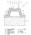
2;シリコン基板
3;多層配線層
4;絶縁層
5;シート層
6;論理回路部
7;温度センサ部
8;CMOSトランジスタ
9、10;チャネル領域
11;絶縁材料
12;差動増幅部
21;電源電位配線
22;接地電位配線
23、24;P型トランジスタ
25、26;N型トランジスタ
31;熱型赤外線検出器
32;シリコン基板
33;赤外線センサ
34;梁
35;赤外線センサ部材
36;絶縁層
37;赤外線の入射方向
38;エアギャップ
39;反射板
G1、G2;ゲート電極
GND;接地電位
N1、N2;n+拡散領域
NW;Nウエル
P1〜P5;p+拡散領域
PW;Pウエル
R1〜R4;温度モニタ部材
V1〜V28;ビア
Vcc;電源電位
Vg;ゲート端子
Vout1、Vout2、Vout3;出力端子
W1、W6、W7、W11、W13、W21、W23、W26、W27;第1配線
W2、W5、W8、W14、W17、W22、W25、W28;第2配線
Claims (13)
- 基板と、前記基板上に設けられた多層配線層と、前記基板の表面及び前記多層配線層に設けられた集積回路部と、を有する集積回路装置であって、
前記集積回路装置は、
前記多層配線層上に設けられた絶縁層と、
前記絶縁層上に設けられ酸化バナジウムにより形成され温度に応じて電気抵抗値が変化するセンサ部材と、
前記絶縁層内に設けられ、前記センサ部材の電極と前記多層配線内の配線とを接続する第1のビアと、
前記センサ部材に接続され前記センサ部材の電気的特性を検出して前記温度を測定する検出手段と、
を有し、
前記センサ部材の断面に流れる電流の最大電流密度が100μA/μm2以下であることを特徴とする集積回路装置。 - 前記センサ部材は、前記第1のビアならびに前記多層配線層内に設けられた複数の第2のビアおよび複数の配線を介して、前記基板に設けられた拡散層に接続されていることを特徴とする請求項1に記載の集積回路装置。
- 前記集積回路装置の外部の温度変化により、前記センサ部材の抵抗値が変化することを特徴とする請求項1又は2に記載の集積回路装置。
- 前記集積回路装置自体の温度変化により、前記センサ部材の抵抗値が変化することを特徴とする請求項1又は2に記載の集積回路装置。
- 前記検出手段の出力に基づいて前記集積回路部が制御されることを特徴とする請求項1乃至4のいずれか1項に記載の集積回路装置。
- 前記センサ部材の直下域に前記集積回路部の少なくとも一部が配置されていることを特徴とする請求項1乃至5のいずれか1項に記載の集積回路装置。
- 複数の前記センサ部材が設けられていることを特徴とする請求項1乃至6のいずれか1項に記載の集積回路装置。
- 前記センサ部材よりも下層に設けられたボンディングパッドを有することを特徴とする請求項1乃至7のいずれか1項に記載の集積回路装置。
- 前記検出手段が前記センサ部材の電気抵抗値を検出するものであることを特徴とする請求項1乃至8のいずれか1項に記載の集積回路装置。
- 前記センサ部材の形状がシート状であることを特徴とする請求項1乃至9のいずれか1項に記載の集積回路装置。
- 電気抵抗値の温度係数の絶対値が前記センサ部材のそれよりも小さい第1及び第2の温度モニタ部材と、差動増幅部と、を有し、前記センサ部材が相互に独立して電流が流れる第3及び第4の温度モニタ部材からなり、第1の基準電位とこの第1の基準電位よりも低い第2の基準電位との間に前記第1及び第3の温度モニタ部材がこの順に直列に接続されて第1の直列接続体が形成され、前記第1の基準電位と前記第2の基準電位との間に前記第4及び第2の温度モニタ部材がこの順に直列に接続されて前記第1の直列接続体に並列に接続された第2の直列接続体が形成され、前記差動増幅部が前記第1の温度モニタ部材と前記第3の温度モニタ部材との間の第1の接続点の電位と前記第4の温度モニタ部材と前記第2の温度モニタ部材との間の第2の接続点の電位との差を増幅するものであることを特徴とする請求項1乃至10のいずれか1項に記載の集積回路装置。
- 前記第1の温度モニタ部材を形成する材料及び形状が前記第2の温度モニタ部材を形成する材料及び形状と夫々等しく、前記第3の温度モニタ部材の形状が前記第4の温度モニタ部材の形状と等しいことを特徴とする請求項11に記載の集積回路装置。
- 前記第1及び第2の温度モニタ部材がシリコンにより形成されていることを特徴とする請求項11又は12に記載の集積回路装置。
Priority Applications (4)
| Application Number | Priority Date | Filing Date | Title |
|---|---|---|---|
| JP2004153456A JP4535367B2 (ja) | 2004-05-24 | 2004-05-24 | 集積回路装置 |
| CNB2005100737767A CN100401472C (zh) | 2004-05-24 | 2005-05-24 | 包括具有受限电流密度的氧化钒传感器元件的半导体器件 |
| US11/135,468 US7544940B2 (en) | 2004-05-24 | 2005-05-24 | Semiconductor device including vanadium oxide sensor element with restricted current density |
| US12/432,102 US20090212385A1 (en) | 2004-05-24 | 2009-04-29 | Semiconductor device including vanadium oxide sensor element with restricted current density |
Applications Claiming Priority (1)
| Application Number | Priority Date | Filing Date | Title |
|---|---|---|---|
| JP2004153456A JP4535367B2 (ja) | 2004-05-24 | 2004-05-24 | 集積回路装置 |
Related Child Applications (1)
| Application Number | Title | Priority Date | Filing Date |
|---|---|---|---|
| JP2010106360A Division JP2010239138A (ja) | 2010-05-06 | 2010-05-06 | 集積回路装置 |
Publications (2)
| Publication Number | Publication Date |
|---|---|
| JP2005340277A JP2005340277A (ja) | 2005-12-08 |
| JP4535367B2 true JP4535367B2 (ja) | 2010-09-01 |
Family
ID=35446675
Family Applications (1)
| Application Number | Title | Priority Date | Filing Date |
|---|---|---|---|
| JP2004153456A Expired - Fee Related JP4535367B2 (ja) | 2004-05-24 | 2004-05-24 | 集積回路装置 |
Country Status (3)
| Country | Link |
|---|---|
| US (2) | US7544940B2 (ja) |
| JP (1) | JP4535367B2 (ja) |
| CN (1) | CN100401472C (ja) |
Families Citing this family (13)
| Publication number | Priority date | Publication date | Assignee | Title |
|---|---|---|---|---|
| JP3810411B2 (ja) * | 2004-01-23 | 2006-08-16 | Necエレクトロニクス株式会社 | 集積回路装置 |
| JP4541717B2 (ja) * | 2004-02-09 | 2010-09-08 | ルネサスエレクトロニクス株式会社 | 集積回路装置及びその製造方法 |
| US7888763B2 (en) * | 2008-02-08 | 2011-02-15 | Omnivision Technologies, Inc. | Backside illuminated imaging sensor with improved infrared sensitivity |
| JP5269527B2 (ja) * | 2008-08-29 | 2013-08-21 | 株式会社東芝 | 半導体装置 |
| US9473714B2 (en) * | 2010-07-01 | 2016-10-18 | Semiconductor Energy Laboratory Co., Ltd. | Solid-state imaging device and semiconductor display device |
| US9331136B2 (en) * | 2014-05-30 | 2016-05-03 | Taiwan Semiconductor Manufacturing Co., Ltd. | Integrated circuit and method of fabricating the same |
| US10501003B2 (en) * | 2015-07-17 | 2019-12-10 | Semiconductor Energy Laboratory Co., Ltd. | Semiconductor device, lighting device, and vehicle |
| TWI627390B (zh) * | 2017-11-20 | 2018-06-21 | 新唐科技股份有限公司 | 操作系統及其控制電路 |
| US11333558B2 (en) | 2018-11-06 | 2022-05-17 | Globalfoundries U.S. Inc. | Boolean temperature sensing using phase transition material |
| JP7120520B2 (ja) * | 2018-11-16 | 2022-08-17 | ミネベアミツミ株式会社 | 湿度検出装置及び温度検出装置 |
| US10931274B2 (en) | 2019-01-18 | 2021-02-23 | Globalfoundries U.S. Inc. | Temperature-sensitive bias circuit |
| EP3973260A4 (en) * | 2019-05-21 | 2023-12-20 | Nextinput, Inc. | COMBINED NEAR AND MID INFRARED SENSOR IN A CHIP-SIZE HOUSING |
| CN110455419B (zh) * | 2019-07-08 | 2020-11-13 | 暨南大学 | 基于氧化钒单晶片的悬空式光电探测器及其制备方法 |
Family Cites Families (24)
| Publication number | Priority date | Publication date | Assignee | Title |
|---|---|---|---|---|
| US4320664A (en) * | 1980-02-25 | 1982-03-23 | Texas Instruments Incorporated | Thermally compensated silicon pressure sensor |
| JPH01302849A (ja) | 1988-05-31 | 1989-12-06 | Fujitsu Ltd | 半導体集積回路装置 |
| FR2639784B1 (fr) * | 1988-11-29 | 1991-01-11 | Commissariat Energie Atomique | Structure monolithique de detection ou d'imagerie infrarouge et son procede de fabrication |
| US5243858A (en) * | 1991-08-12 | 1993-09-14 | General Motors Corporation | Fluid flow sensor with thermistor detector |
| EP0566156B1 (en) * | 1992-04-17 | 1997-08-27 | Terumo Kabushiki Kaisha | Infrared sensor and method for production thereof |
| CA2150502A1 (en) * | 1994-08-05 | 1996-02-06 | Michael F. Mattes | Method and apparatus for measuring temperature |
| JP2710228B2 (ja) * | 1994-08-11 | 1998-02-10 | 日本電気株式会社 | ボロメータ型赤外線検知素子、その駆動方法、および検出用積分回路 |
| US5639163A (en) * | 1994-11-14 | 1997-06-17 | International Business Machines Corporation | On-chip temperature sensing system |
| GB9513420D0 (en) * | 1995-06-30 | 1995-09-06 | Philips Electronics Uk Ltd | Power semiconductor devices |
| JPH09229778A (ja) | 1996-02-26 | 1997-09-05 | Hitachi Ltd | Ic化温度センサ |
| JP3040356B2 (ja) * | 1997-01-27 | 2000-05-15 | 三菱電機株式会社 | 赤外線固体撮像素子 |
| JPH11118567A (ja) | 1997-10-09 | 1999-04-30 | Tokyo Gas Co Ltd | フローセンサ |
| JP3067737B2 (ja) | 1998-05-18 | 2000-07-24 | 日本電気株式会社 | 酸化バナジウム膜のプラズマエッチング方法 |
| US6504222B1 (en) * | 1998-12-28 | 2003-01-07 | Fujitsu Limited | Multi-quantum well infrared photo-detector |
| JP3460810B2 (ja) | 1999-07-26 | 2003-10-27 | 日本電気株式会社 | 熱分離構造を有する熱型赤外線検出器 |
| KR20010092770A (ko) * | 1999-11-01 | 2001-10-26 | 모리시타 요이찌 | 반도체 장치 및 그 제조방법 |
| JP3921320B2 (ja) * | 2000-01-31 | 2007-05-30 | 日本電気株式会社 | 熱型赤外線検出器およびその製造方法 |
| US6610984B2 (en) * | 2000-03-17 | 2003-08-26 | Infrared Components Corporation | Method and apparatus for correction of microbolometer output |
| JP3783834B2 (ja) | 2000-04-26 | 2006-06-07 | 三菱電機株式会社 | 赤外線検知素子の製造方法 |
| JP2002267530A (ja) | 2001-03-07 | 2002-09-18 | Mitsubishi Electric Corp | 赤外線検知素子の製造方法及び赤外線検知素子 |
| US6777681B1 (en) * | 2001-04-25 | 2004-08-17 | Raytheon Company | Infrared detector with amorphous silicon detector elements, and a method of making it |
| US20020166968A1 (en) * | 2001-05-11 | 2002-11-14 | Bradley Martin G. | Apparatus and method of measuring bolometric resistance changes in an uncooled and thermally unstabilized focal plane array over a wide temperature range |
| JP4236402B2 (ja) * | 2001-10-09 | 2009-03-11 | 富士通マイクロエレクトロニクス株式会社 | 半導体装置 |
| JP3859479B2 (ja) * | 2001-10-17 | 2006-12-20 | 日本電気株式会社 | ボロメータ型赤外線検出器 |
-
2004
- 2004-05-24 JP JP2004153456A patent/JP4535367B2/ja not_active Expired - Fee Related
-
2005
- 2005-05-24 US US11/135,468 patent/US7544940B2/en not_active Expired - Fee Related
- 2005-05-24 CN CNB2005100737767A patent/CN100401472C/zh not_active Expired - Fee Related
-
2009
- 2009-04-29 US US12/432,102 patent/US20090212385A1/en not_active Abandoned
Also Published As
| Publication number | Publication date |
|---|---|
| US20050269512A1 (en) | 2005-12-08 |
| US20090212385A1 (en) | 2009-08-27 |
| CN100401472C (zh) | 2008-07-09 |
| JP2005340277A (ja) | 2005-12-08 |
| US7544940B2 (en) | 2009-06-09 |
| CN1716536A (zh) | 2006-01-04 |
Similar Documents
| Publication | Publication Date | Title |
|---|---|---|
| JP4535367B2 (ja) | 集積回路装置 | |
| JP5028748B2 (ja) | パワー半導体デバイスの温度計測装置 | |
| KR101199904B1 (ko) | 적외선 센서 | |
| KR20110066187A (ko) | 적외선 센서 | |
| JP4806231B2 (ja) | 集積炭素ナノチューブセンサ | |
| US20120085907A1 (en) | Infrared array sensor | |
| JP5530274B2 (ja) | 温度センサ | |
| JP3869815B2 (ja) | 半導体集積回路装置 | |
| JP4536408B2 (ja) | 集積回路装置 | |
| JP5261102B2 (ja) | 赤外線センサおよび赤外線センサモジュール | |
| JP3810411B2 (ja) | 集積回路装置 | |
| CN116298456A (zh) | 电流测量电路 | |
| JP2010239138A (ja) | 集積回路装置 | |
| US8562210B2 (en) | Thermal sensor for semiconductor circuits | |
| JP5256862B2 (ja) | 撮像デバイス | |
| JP3237256B2 (ja) | 加速度検出回路 | |
| JP4541717B2 (ja) | 集積回路装置及びその製造方法 | |
| JP2007225398A (ja) | 熱型赤外線検出器および熱型赤外線センサ | |
| JP5081116B2 (ja) | 赤外線センサおよび赤外線センサモジュール | |
| JP5629146B2 (ja) | 温度センサ | |
| JP5261447B2 (ja) | 赤外線センサ | |
| JP2009111290A (ja) | 抵抗測定素子およびコンタクト抵抗の測定方法、並びに半導体素子チップおよびその評価方法 | |
| JP2001021610A (ja) | 半導体装置 |
Legal Events
| Date | Code | Title | Description |
|---|---|---|---|
| A977 | Report on retrieval |
Free format text: JAPANESE INTERMEDIATE CODE: A971007 Effective date: 20060616 |
|
| A131 | Notification of reasons for refusal |
Free format text: JAPANESE INTERMEDIATE CODE: A131 Effective date: 20060627 |
|
| RD02 | Notification of acceptance of power of attorney |
Free format text: JAPANESE INTERMEDIATE CODE: A7422 Effective date: 20070112 |
|
| A02 | Decision of refusal |
Free format text: JAPANESE INTERMEDIATE CODE: A02 Effective date: 20070320 |
|
| RD01 | Notification of change of attorney |
Free format text: JAPANESE INTERMEDIATE CODE: A7421 Effective date: 20070419 |
|
| A521 | Request for written amendment filed |
Free format text: JAPANESE INTERMEDIATE CODE: A523 Effective date: 20070518 |
|
| A521 | Request for written amendment filed |
Free format text: JAPANESE INTERMEDIATE CODE: A821 Effective date: 20070419 |
|
| A911 | Transfer to examiner for re-examination before appeal (zenchi) |
Free format text: JAPANESE INTERMEDIATE CODE: A911 Effective date: 20070531 |
|
| RD01 | Notification of change of attorney |
Free format text: JAPANESE INTERMEDIATE CODE: A7421 Effective date: 20070703 |
|
| A912 | Re-examination (zenchi) completed and case transferred to appeal board |
Free format text: JAPANESE INTERMEDIATE CODE: A912 Effective date: 20070706 |
|
| RD01 | Notification of change of attorney |
Free format text: JAPANESE INTERMEDIATE CODE: A7421 Effective date: 20100426 |
|
| A521 | Request for written amendment filed |
Free format text: JAPANESE INTERMEDIATE CODE: A523 Effective date: 20100506 |
|
| A01 | Written decision to grant a patent or to grant a registration (utility model) |
Free format text: JAPANESE INTERMEDIATE CODE: A01 |
|
| A61 | First payment of annual fees (during grant procedure) |
Free format text: JAPANESE INTERMEDIATE CODE: A61 Effective date: 20100610 |
|
| FPAY | Renewal fee payment (event date is renewal date of database) |
Free format text: PAYMENT UNTIL: 20130625 Year of fee payment: 3 |
|
| R150 | Certificate of patent or registration of utility model |
Ref document number: 4535367 Country of ref document: JP Free format text: JAPANESE INTERMEDIATE CODE: R150 Free format text: JAPANESE INTERMEDIATE CODE: R150 |
|
| FPAY | Renewal fee payment (event date is renewal date of database) |
Free format text: PAYMENT UNTIL: 20130625 Year of fee payment: 3 |
|
| FPAY | Renewal fee payment (event date is renewal date of database) |
Free format text: PAYMENT UNTIL: 20140625 Year of fee payment: 4 |
|
| S531 | Written request for registration of change of domicile |
Free format text: JAPANESE INTERMEDIATE CODE: R313531 |
|
| R350 | Written notification of registration of transfer |
Free format text: JAPANESE INTERMEDIATE CODE: R350 |
|
| LAPS | Cancellation because of no payment of annual fees |