JP4628954B2 - 酸化物薄膜製造方法 - Google Patents
酸化物薄膜製造方法 Download PDFInfo
- Publication number
- JP4628954B2 JP4628954B2 JP2005513346A JP2005513346A JP4628954B2 JP 4628954 B2 JP4628954 B2 JP 4628954B2 JP 2005513346 A JP2005513346 A JP 2005513346A JP 2005513346 A JP2005513346 A JP 2005513346A JP 4628954 B2 JP4628954 B2 JP 4628954B2
- Authority
- JP
- Japan
- Prior art keywords
- gas
- thin film
- oxide thin
- flow rate
- substrate
- Prior art date
- Legal status (The legal status is an assumption and is not a legal conclusion. Google has not performed a legal analysis and makes no representation as to the accuracy of the status listed.)
- Expired - Lifetime
Links
Images






Classifications
-
- C—CHEMISTRY; METALLURGY
- C23—COATING METALLIC MATERIAL; COATING MATERIAL WITH METALLIC MATERIAL; CHEMICAL SURFACE TREATMENT; DIFFUSION TREATMENT OF METALLIC MATERIAL; COATING BY VACUUM EVAPORATION, BY SPUTTERING, BY ION IMPLANTATION OR BY CHEMICAL VAPOUR DEPOSITION, IN GENERAL; INHIBITING CORROSION OF METALLIC MATERIAL OR INCRUSTATION IN GENERAL
- C23C—COATING METALLIC MATERIAL; COATING MATERIAL WITH METALLIC MATERIAL; SURFACE TREATMENT OF METALLIC MATERIAL BY DIFFUSION INTO THE SURFACE, BY CHEMICAL CONVERSION OR SUBSTITUTION; COATING BY VACUUM EVAPORATION, BY SPUTTERING, BY ION IMPLANTATION OR BY CHEMICAL VAPOUR DEPOSITION, IN GENERAL
- C23C16/00—Chemical coating by decomposition of gaseous compounds, without leaving reaction products of surface material in the coating, i.e. chemical vapour deposition [CVD] processes
- C23C16/22—Chemical coating by decomposition of gaseous compounds, without leaving reaction products of surface material in the coating, i.e. chemical vapour deposition [CVD] processes characterised by the deposition of inorganic material, other than metallic material
- C23C16/30—Deposition of compounds, mixtures or solid solutions, e.g. borides, carbides, nitrides
- C23C16/40—Oxides
- C23C16/409—Oxides of the type ABO3 with A representing alkali, alkaline earth metal or lead and B representing a refractory metal, nickel, scandium or a lanthanide
-
- H—ELECTRICITY
- H10—SEMICONDUCTOR DEVICES; ELECTRIC SOLID-STATE DEVICES NOT OTHERWISE PROVIDED FOR
- H10P—GENERIC PROCESSES OR APPARATUS FOR THE MANUFACTURE OR TREATMENT OF DEVICES COVERED BY CLASS H10
- H10P14/00—Formation of materials, e.g. in the shape of layers or pillars
- H10P14/60—Formation of materials, e.g. in the shape of layers or pillars of insulating materials
- H10P14/63—Formation of materials, e.g. in the shape of layers or pillars of insulating materials characterised by the formation processes
- H10P14/6326—Deposition processes
- H10P14/6328—Deposition from the gas or vapour phase
- H10P14/6334—Deposition from the gas or vapour phase using decomposition or reaction of gaseous or vapour phase compounds, i.e. chemical vapour deposition
-
- C—CHEMISTRY; METALLURGY
- C23—COATING METALLIC MATERIAL; COATING MATERIAL WITH METALLIC MATERIAL; CHEMICAL SURFACE TREATMENT; DIFFUSION TREATMENT OF METALLIC MATERIAL; COATING BY VACUUM EVAPORATION, BY SPUTTERING, BY ION IMPLANTATION OR BY CHEMICAL VAPOUR DEPOSITION, IN GENERAL; INHIBITING CORROSION OF METALLIC MATERIAL OR INCRUSTATION IN GENERAL
- C23C—COATING METALLIC MATERIAL; COATING MATERIAL WITH METALLIC MATERIAL; SURFACE TREATMENT OF METALLIC MATERIAL BY DIFFUSION INTO THE SURFACE, BY CHEMICAL CONVERSION OR SUBSTITUTION; COATING BY VACUUM EVAPORATION, BY SPUTTERING, BY ION IMPLANTATION OR BY CHEMICAL VAPOUR DEPOSITION, IN GENERAL
- C23C16/00—Chemical coating by decomposition of gaseous compounds, without leaving reaction products of surface material in the coating, i.e. chemical vapour deposition [CVD] processes
- C23C16/02—Pretreatment of the material to be coated
- C23C16/0272—Deposition of sub-layers, e.g. to promote the adhesion of the main coating
-
- C—CHEMISTRY; METALLURGY
- C23—COATING METALLIC MATERIAL; COATING MATERIAL WITH METALLIC MATERIAL; CHEMICAL SURFACE TREATMENT; DIFFUSION TREATMENT OF METALLIC MATERIAL; COATING BY VACUUM EVAPORATION, BY SPUTTERING, BY ION IMPLANTATION OR BY CHEMICAL VAPOUR DEPOSITION, IN GENERAL; INHIBITING CORROSION OF METALLIC MATERIAL OR INCRUSTATION IN GENERAL
- C23C—COATING METALLIC MATERIAL; COATING MATERIAL WITH METALLIC MATERIAL; SURFACE TREATMENT OF METALLIC MATERIAL BY DIFFUSION INTO THE SURFACE, BY CHEMICAL CONVERSION OR SUBSTITUTION; COATING BY VACUUM EVAPORATION, BY SPUTTERING, BY ION IMPLANTATION OR BY CHEMICAL VAPOUR DEPOSITION, IN GENERAL
- C23C16/00—Chemical coating by decomposition of gaseous compounds, without leaving reaction products of surface material in the coating, i.e. chemical vapour deposition [CVD] processes
- C23C16/44—Chemical coating by decomposition of gaseous compounds, without leaving reaction products of surface material in the coating, i.e. chemical vapour deposition [CVD] processes characterised by the method of coating
- C23C16/448—Chemical coating by decomposition of gaseous compounds, without leaving reaction products of surface material in the coating, i.e. chemical vapour deposition [CVD] processes characterised by the method of coating characterised by the method used for generating reactive gas streams, e.g. by evaporation or sublimation of precursor materials
- C23C16/4481—Chemical coating by decomposition of gaseous compounds, without leaving reaction products of surface material in the coating, i.e. chemical vapour deposition [CVD] processes characterised by the method of coating characterised by the method used for generating reactive gas streams, e.g. by evaporation or sublimation of precursor materials by evaporation using carrier gas in contact with the source material
- C23C16/4482—Chemical coating by decomposition of gaseous compounds, without leaving reaction products of surface material in the coating, i.e. chemical vapour deposition [CVD] processes characterised by the method of coating characterised by the method used for generating reactive gas streams, e.g. by evaporation or sublimation of precursor materials by evaporation using carrier gas in contact with the source material by bubbling of carrier gas through liquid source material
-
- C—CHEMISTRY; METALLURGY
- C23—COATING METALLIC MATERIAL; COATING MATERIAL WITH METALLIC MATERIAL; CHEMICAL SURFACE TREATMENT; DIFFUSION TREATMENT OF METALLIC MATERIAL; COATING BY VACUUM EVAPORATION, BY SPUTTERING, BY ION IMPLANTATION OR BY CHEMICAL VAPOUR DEPOSITION, IN GENERAL; INHIBITING CORROSION OF METALLIC MATERIAL OR INCRUSTATION IN GENERAL
- C23C—COATING METALLIC MATERIAL; COATING MATERIAL WITH METALLIC MATERIAL; SURFACE TREATMENT OF METALLIC MATERIAL BY DIFFUSION INTO THE SURFACE, BY CHEMICAL CONVERSION OR SUBSTITUTION; COATING BY VACUUM EVAPORATION, BY SPUTTERING, BY ION IMPLANTATION OR BY CHEMICAL VAPOUR DEPOSITION, IN GENERAL
- C23C16/00—Chemical coating by decomposition of gaseous compounds, without leaving reaction products of surface material in the coating, i.e. chemical vapour deposition [CVD] processes
- C23C16/44—Chemical coating by decomposition of gaseous compounds, without leaving reaction products of surface material in the coating, i.e. chemical vapour deposition [CVD] processes characterised by the method of coating
- C23C16/448—Chemical coating by decomposition of gaseous compounds, without leaving reaction products of surface material in the coating, i.e. chemical vapour deposition [CVD] processes characterised by the method of coating characterised by the method used for generating reactive gas streams, e.g. by evaporation or sublimation of precursor materials
- C23C16/452—Chemical coating by decomposition of gaseous compounds, without leaving reaction products of surface material in the coating, i.e. chemical vapour deposition [CVD] processes characterised by the method of coating characterised by the method used for generating reactive gas streams, e.g. by evaporation or sublimation of precursor materials by activating reactive gas streams before their introduction into the reaction chamber, e.g. by ionisation or addition of reactive species
-
- H—ELECTRICITY
- H10—SEMICONDUCTOR DEVICES; ELECTRIC SOLID-STATE DEVICES NOT OTHERWISE PROVIDED FOR
- H10P—GENERIC PROCESSES OR APPARATUS FOR THE MANUFACTURE OR TREATMENT OF DEVICES COVERED BY CLASS H10
- H10P14/00—Formation of materials, e.g. in the shape of layers or pillars
- H10P14/60—Formation of materials, e.g. in the shape of layers or pillars of insulating materials
- H10P14/65—Formation of materials, e.g. in the shape of layers or pillars of insulating materials characterised by treatments performed before or after the formation of the materials
- H10P14/6502—Formation of materials, e.g. in the shape of layers or pillars of insulating materials characterised by treatments performed before or after the formation of the materials of treatments performed before formation of the materials
- H10P14/6506—Formation of intermediate materials
-
- H—ELECTRICITY
- H10—SEMICONDUCTOR DEVICES; ELECTRIC SOLID-STATE DEVICES NOT OTHERWISE PROVIDED FOR
- H10P—GENERIC PROCESSES OR APPARATUS FOR THE MANUFACTURE OR TREATMENT OF DEVICES COVERED BY CLASS H10
- H10P14/00—Formation of materials, e.g. in the shape of layers or pillars
- H10P14/60—Formation of materials, e.g. in the shape of layers or pillars of insulating materials
- H10P14/69—Inorganic materials
- H10P14/692—Inorganic materials composed of oxides, glassy oxides or oxide-based glasses
- H10P14/6921—Inorganic materials composed of oxides, glassy oxides or oxide-based glasses containing silicon
- H10P14/69215—Inorganic materials composed of oxides, glassy oxides or oxide-based glasses containing silicon the material being a silicon oxide, e.g. SiO2
-
- H—ELECTRICITY
- H10—SEMICONDUCTOR DEVICES; ELECTRIC SOLID-STATE DEVICES NOT OTHERWISE PROVIDED FOR
- H10P—GENERIC PROCESSES OR APPARATUS FOR THE MANUFACTURE OR TREATMENT OF DEVICES COVERED BY CLASS H10
- H10P14/00—Formation of materials, e.g. in the shape of layers or pillars
- H10P14/60—Formation of materials, e.g. in the shape of layers or pillars of insulating materials
- H10P14/69—Inorganic materials
- H10P14/692—Inorganic materials composed of oxides, glassy oxides or oxide-based glasses
- H10P14/6938—Inorganic materials composed of oxides, glassy oxides or oxide-based glasses the material containing at least one metal element, e.g. metal oxides, metal oxynitrides or metal oxycarbides
- H10P14/6939—Inorganic materials composed of oxides, glassy oxides or oxide-based glasses the material containing at least one metal element, e.g. metal oxides, metal oxynitrides or metal oxycarbides characterised by the metal
-
- H—ELECTRICITY
- H10—SEMICONDUCTOR DEVICES; ELECTRIC SOLID-STATE DEVICES NOT OTHERWISE PROVIDED FOR
- H10P—GENERIC PROCESSES OR APPARATUS FOR THE MANUFACTURE OR TREATMENT OF DEVICES COVERED BY CLASS H10
- H10P14/00—Formation of materials, e.g. in the shape of layers or pillars
- H10P14/60—Formation of materials, e.g. in the shape of layers or pillars of insulating materials
- H10P14/69—Inorganic materials
- H10P14/692—Inorganic materials composed of oxides, glassy oxides or oxide-based glasses
- H10P14/6938—Inorganic materials composed of oxides, glassy oxides or oxide-based glasses the material containing at least one metal element, e.g. metal oxides, metal oxynitrides or metal oxycarbides
- H10P14/6939—Inorganic materials composed of oxides, glassy oxides or oxide-based glasses the material containing at least one metal element, e.g. metal oxides, metal oxynitrides or metal oxycarbides characterised by the metal
- H10P14/69391—Inorganic materials composed of oxides, glassy oxides or oxide-based glasses the material containing at least one metal element, e.g. metal oxides, metal oxynitrides or metal oxycarbides characterised by the metal the material containing aluminium, e.g. Al2O3
-
- H—ELECTRICITY
- H10—SEMICONDUCTOR DEVICES; ELECTRIC SOLID-STATE DEVICES NOT OTHERWISE PROVIDED FOR
- H10P—GENERIC PROCESSES OR APPARATUS FOR THE MANUFACTURE OR TREATMENT OF DEVICES COVERED BY CLASS H10
- H10P14/00—Formation of materials, e.g. in the shape of layers or pillars
- H10P14/60—Formation of materials, e.g. in the shape of layers or pillars of insulating materials
- H10P14/69—Inorganic materials
- H10P14/692—Inorganic materials composed of oxides, glassy oxides or oxide-based glasses
- H10P14/6938—Inorganic materials composed of oxides, glassy oxides or oxide-based glasses the material containing at least one metal element, e.g. metal oxides, metal oxynitrides or metal oxycarbides
- H10P14/6939—Inorganic materials composed of oxides, glassy oxides or oxide-based glasses the material containing at least one metal element, e.g. metal oxides, metal oxynitrides or metal oxycarbides characterised by the metal
- H10P14/69392—Inorganic materials composed of oxides, glassy oxides or oxide-based glasses the material containing at least one metal element, e.g. metal oxides, metal oxynitrides or metal oxycarbides characterised by the metal the material containing hafnium, e.g. HfO2
-
- H—ELECTRICITY
- H10—SEMICONDUCTOR DEVICES; ELECTRIC SOLID-STATE DEVICES NOT OTHERWISE PROVIDED FOR
- H10P—GENERIC PROCESSES OR APPARATUS FOR THE MANUFACTURE OR TREATMENT OF DEVICES COVERED BY CLASS H10
- H10P14/00—Formation of materials, e.g. in the shape of layers or pillars
- H10P14/60—Formation of materials, e.g. in the shape of layers or pillars of insulating materials
- H10P14/69—Inorganic materials
- H10P14/692—Inorganic materials composed of oxides, glassy oxides or oxide-based glasses
- H10P14/6938—Inorganic materials composed of oxides, glassy oxides or oxide-based glasses the material containing at least one metal element, e.g. metal oxides, metal oxynitrides or metal oxycarbides
- H10P14/6939—Inorganic materials composed of oxides, glassy oxides or oxide-based glasses the material containing at least one metal element, e.g. metal oxides, metal oxynitrides or metal oxycarbides characterised by the metal
- H10P14/69393—Inorganic materials composed of oxides, glassy oxides or oxide-based glasses the material containing at least one metal element, e.g. metal oxides, metal oxynitrides or metal oxycarbides characterised by the metal the material containing tantalum, e.g. Ta2O5
-
- H—ELECTRICITY
- H10—SEMICONDUCTOR DEVICES; ELECTRIC SOLID-STATE DEVICES NOT OTHERWISE PROVIDED FOR
- H10P—GENERIC PROCESSES OR APPARATUS FOR THE MANUFACTURE OR TREATMENT OF DEVICES COVERED BY CLASS H10
- H10P14/00—Formation of materials, e.g. in the shape of layers or pillars
- H10P14/60—Formation of materials, e.g. in the shape of layers or pillars of insulating materials
- H10P14/69—Inorganic materials
- H10P14/692—Inorganic materials composed of oxides, glassy oxides or oxide-based glasses
- H10P14/6938—Inorganic materials composed of oxides, glassy oxides or oxide-based glasses the material containing at least one metal element, e.g. metal oxides, metal oxynitrides or metal oxycarbides
- H10P14/6939—Inorganic materials composed of oxides, glassy oxides or oxide-based glasses the material containing at least one metal element, e.g. metal oxides, metal oxynitrides or metal oxycarbides characterised by the metal
- H10P14/69394—Inorganic materials composed of oxides, glassy oxides or oxide-based glasses the material containing at least one metal element, e.g. metal oxides, metal oxynitrides or metal oxycarbides characterised by the metal the material containing titanium, e.g. TiO2
-
- H—ELECTRICITY
- H10—SEMICONDUCTOR DEVICES; ELECTRIC SOLID-STATE DEVICES NOT OTHERWISE PROVIDED FOR
- H10P—GENERIC PROCESSES OR APPARATUS FOR THE MANUFACTURE OR TREATMENT OF DEVICES COVERED BY CLASS H10
- H10P14/00—Formation of materials, e.g. in the shape of layers or pillars
- H10P14/60—Formation of materials, e.g. in the shape of layers or pillars of insulating materials
- H10P14/69—Inorganic materials
- H10P14/692—Inorganic materials composed of oxides, glassy oxides or oxide-based glasses
- H10P14/6938—Inorganic materials composed of oxides, glassy oxides or oxide-based glasses the material containing at least one metal element, e.g. metal oxides, metal oxynitrides or metal oxycarbides
- H10P14/6939—Inorganic materials composed of oxides, glassy oxides or oxide-based glasses the material containing at least one metal element, e.g. metal oxides, metal oxynitrides or metal oxycarbides characterised by the metal
- H10P14/69395—Inorganic materials composed of oxides, glassy oxides or oxide-based glasses the material containing at least one metal element, e.g. metal oxides, metal oxynitrides or metal oxycarbides characterised by the metal the material containing zirconium, e.g. ZrO2
-
- H—ELECTRICITY
- H10—SEMICONDUCTOR DEVICES; ELECTRIC SOLID-STATE DEVICES NOT OTHERWISE PROVIDED FOR
- H10P—GENERIC PROCESSES OR APPARATUS FOR THE MANUFACTURE OR TREATMENT OF DEVICES COVERED BY CLASS H10
- H10P14/00—Formation of materials, e.g. in the shape of layers or pillars
- H10P14/60—Formation of materials, e.g. in the shape of layers or pillars of insulating materials
- H10P14/69—Inorganic materials
- H10P14/692—Inorganic materials composed of oxides, glassy oxides or oxide-based glasses
- H10P14/6938—Inorganic materials composed of oxides, glassy oxides or oxide-based glasses the material containing at least one metal element, e.g. metal oxides, metal oxynitrides or metal oxycarbides
- H10P14/69398—Inorganic materials composed of oxides, glassy oxides or oxide-based glasses the material containing at least one metal element, e.g. metal oxides, metal oxynitrides or metal oxycarbides the material having a perovskite structure, e.g. BaTiO3
Landscapes
- Chemical & Material Sciences (AREA)
- Mechanical Engineering (AREA)
- General Chemical & Material Sciences (AREA)
- Chemical Kinetics & Catalysis (AREA)
- Engineering & Computer Science (AREA)
- Materials Engineering (AREA)
- Metallurgy (AREA)
- Organic Chemistry (AREA)
- Inorganic Chemistry (AREA)
- Semiconductor Memories (AREA)
- Formation Of Insulating Films (AREA)
- Chemical Vapour Deposition (AREA)
- Crystals, And After-Treatments Of Crystals (AREA)
Description

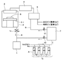
2 反応室 3 シャワープレート
4 ガス活性化手段 5 ガス混合器
6 原料ガス配管 7 気化器
7a 原料供給部 8 配管
S 基板
Claims (9)
- 酸化物薄膜用原料を気化した原料ガス、キャリアガス及び酸化ガスをガス混合器で混合し、得られた混合ガスをシャワープレートを通して化学気相成長装置の反応室内で加熱された基板上に供給して反応させ、基板上に酸化物薄膜を製造する方法において、
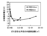
前記ガス混合器と前記シャワープレートとの間に設けられ、内壁表面積が4.8×10⁻³m2〜1.28×10⁻¹m2である配管を備え、シャワープレートへ導入される際の原料ガスが所望の膜特性が得られる金属原子含有分子に気相分解される温度に加熱されたガス活性化手段を通して、前記混合ガスを前記反応室内に供給し、
前記酸化ガスの流量割合が混合ガス基準で60%以上であることを特徴とする酸化物薄膜製造方法。 - 酸化物薄膜用原料を気化した原料ガス、キャリアガス及び酸化ガスをガス混合器で混合し、得られた混合ガスをシャワープレートを通して化学気相成長装置の反応室内で加熱された基板上に供給して反応させ、基板上に酸化物薄膜を製造する方法において、
前記混合ガスを前記ガス混合器と前記シャワープレートとの間に設けられたガス活性化手段を通して反応室内に供給するものであって、
前記混合ガスを前記反応室内に供給してシード層としての初期層を成膜する工程と、
前記初期層を成膜する工程で供給された混合ガスよりも高い酸化ガス流量割合を有する混合ガスを前記反応室内に供給して前記初期層の上に第二層を連続して成膜する工程と、を含むことを特徴とする酸化物薄膜製造方法。 - 前記初期層を成膜する工程における酸化ガスの流量割合が混合ガス基準で60%未満であり、前記第二層を成膜する工程における酸化ガスの流量割合が混合ガス基準で60%以上であることを特徴とする請求項2記載の酸化物薄膜製造方法。
- 前記ガス活性化手段が、シャワープレートへ導入される際の原料ガスが所望の膜特性が得られる金属原子含有分子に気相分解される温度に維持されていることを特徴とする請求項2または請求項3記載の酸化物薄膜製造方法。
- 前記酸化ガスは、酸素、オゾン、N2O、及びNO2から選ばれたガスであることを特徴とする請求項1乃至請求項4のいずれか1項記載の酸化物薄膜製造方法。
- 前記キャリアガスは、窒素、ヘリウム、アルゴン、ネオン、クリプトンから選ばれた不活性ガスであることを特徴とする請求項1乃至請求項5のいずれか1項記載の酸化物薄膜製造方法。
- 前記基板は、Pt、Ir、Rh、Ru、MgO、SrTiO3、IrO2、RuO2、SrRuO3、及びLaNiO3から選ばれた材料からなる電極を有し、この電極の上に前記酸化物薄膜を製造することを特徴とする請求項1乃至請求項6のいずれか1項記載の酸化物薄膜製造方法。
- 前記酸化物薄膜は、SiO2、TiO2、Al2O3、Ta2O5、MgO、ZrO2、HfO2、(Ba,Sr)TiO2、及びSrTiO3から選ばれた常誘電体酸化物、または、Pb(Zr,Ti)O3、SrBi2Ta2O9、及びBi4Ti3O12から選ばれた強誘電体酸化物からなることを特徴とする請求項1乃至請求項7のいずれか1項記載の酸化物薄膜製造方法。
- 製造する酸化物薄膜中の所定の原子が基板中へ拡散しやすい場合、初期層中のその原子の量を拡散しにくい基板の場合より多くすることによりエピタキシャル成長を実現することを特徴とする請求項1乃至請求項8のいずれか1項記載の酸化物薄膜製造方法。
Applications Claiming Priority (3)
| Application Number | Priority Date | Filing Date | Title |
|---|---|---|---|
| JP2003300014 | 2003-08-25 | ||
| JP2003300014 | 2003-08-25 | ||
| PCT/JP2004/012180 WO2005020311A1 (ja) | 2003-08-25 | 2004-08-25 | 酸化物薄膜製造方法及びその製造装置 |
Publications (2)
| Publication Number | Publication Date |
|---|---|
| JPWO2005020311A1 JPWO2005020311A1 (ja) | 2007-11-01 |
| JP4628954B2 true JP4628954B2 (ja) | 2011-02-09 |
Family
ID=34213796
Family Applications (1)
| Application Number | Title | Priority Date | Filing Date |
|---|---|---|---|
| JP2005513346A Expired - Lifetime JP4628954B2 (ja) | 2003-08-25 | 2004-08-25 | 酸化物薄膜製造方法 |
Country Status (7)
| Country | Link |
|---|---|
| US (1) | US20070054472A1 (ja) |
| EP (1) | EP1662556B1 (ja) |
| JP (1) | JP4628954B2 (ja) |
| KR (2) | KR101179098B1 (ja) |
| CN (1) | CN100435294C (ja) |
| TW (1) | TW200511404A (ja) |
| WO (1) | WO2005020311A1 (ja) |
Families Citing this family (8)
| Publication number | Priority date | Publication date | Assignee | Title |
|---|---|---|---|---|
| JP2008053683A (ja) * | 2006-07-27 | 2008-03-06 | Matsushita Electric Ind Co Ltd | 絶縁膜形成方法、半導体装置、および基板処理装置 |
| EP2053642A4 (en) * | 2006-08-02 | 2011-01-05 | Ulvac Inc | FILM-EDGING METHOD AND FILM-EDITING DEVICE |
| JP2010080813A (ja) * | 2008-09-29 | 2010-04-08 | Fujifilm Corp | 圧電体膜とその製造方法、圧電素子、及び液体吐出装置 |
| TWI452946B (zh) * | 2009-12-29 | 2014-09-11 | Univ Nat Yunlin Sci & Tech | Plasma reaction device |
| JP2014150191A (ja) * | 2013-02-01 | 2014-08-21 | Ulvac Japan Ltd | Pzt膜の製造方法及び成膜装置 |
| CN106367732B (zh) * | 2016-09-22 | 2018-11-06 | 四川大学 | 一种中温金属有机化学气相沉积TiO2-Al2O3复合涂层装置及涂覆方法 |
| CN110586180B (zh) * | 2019-09-20 | 2022-06-14 | 湖南师范大学 | 一种具有可见光催化n2o参与选择性氧化的钌杂化十聚钨酸季铵盐的制备方法 |
| KR102937892B1 (ko) * | 2020-12-07 | 2026-03-11 | 주식회사 원익아이피에스 | 기판 처리 장치 |
Citations (6)
| Publication number | Priority date | Publication date | Assignee | Title |
|---|---|---|---|---|
| JPH0883793A (ja) * | 1994-06-08 | 1996-03-26 | Hyundai Electron Ind Co Ltd | 強誘電体薄膜の形成方法 |
| JPH08268797A (ja) * | 1995-03-30 | 1996-10-15 | Hitachi Ltd | 化学気相反応堆積装置 |
| JPH11126877A (ja) * | 1997-07-18 | 1999-05-11 | Ramtron Internatl Corp | 強誘電性薄膜の性能を最適化するための多層方式 |
| JP2000058525A (ja) * | 1998-08-03 | 2000-02-25 | Nec Corp | 金属酸化物誘電体膜の気相成長方法 |
| JP2003086586A (ja) * | 2001-09-13 | 2003-03-20 | Murata Mfg Co Ltd | 配向性強誘電体薄膜素子及びその製造方法 |
| JP2003324101A (ja) * | 2002-04-30 | 2003-11-14 | Fujitsu Ltd | 半導体装置の製造方法 |
Family Cites Families (9)
| Publication number | Priority date | Publication date | Assignee | Title |
|---|---|---|---|---|
| JPH086181B2 (ja) * | 1992-11-30 | 1996-01-24 | 日本電気株式会社 | 化学気相成長法および化学気相成長装置 |
| US5989998A (en) * | 1996-08-29 | 1999-11-23 | Matsushita Electric Industrial Co., Ltd. | Method of forming interlayer insulating film |
| JPH1131650A (ja) * | 1997-07-14 | 1999-02-02 | Kokusai Electric Co Ltd | 反射防止膜、被処理基板、被処理基板の製造方法、微細パターンの製造方法、および半導体装置の製造方法 |
| WO2000036640A1 (en) * | 1998-12-16 | 2000-06-22 | Tokyo Electron Limited | Method of forming thin film |
| US6495878B1 (en) * | 1999-08-02 | 2002-12-17 | Symetrix Corporation | Interlayer oxide containing thin films for high dielectric constant application |
| US6811651B2 (en) * | 2001-06-22 | 2004-11-02 | Tokyo Electron Limited | Gas temperature control for a plasma process |
| US20030012875A1 (en) * | 2001-07-10 | 2003-01-16 | Shreyas Kher | CVD BST film composition and property control with thickness below 200 A for DRAM capacitor application with size at 0.1mum or below |
| US6713127B2 (en) * | 2001-12-28 | 2004-03-30 | Applied Materials, Inc. | Methods for silicon oxide and oxynitride deposition using single wafer low pressure CVD |
| US6884464B2 (en) * | 2002-11-04 | 2005-04-26 | Applied Materials, Inc. | Methods for forming silicon comprising films using hexachlorodisilane in a single-wafer deposion chamber |
-
2004
- 2004-08-25 JP JP2005513346A patent/JP4628954B2/ja not_active Expired - Lifetime
- 2004-08-25 EP EP04772141.0A patent/EP1662556B1/en not_active Expired - Lifetime
- 2004-08-25 WO PCT/JP2004/012180 patent/WO2005020311A1/ja not_active Ceased
- 2004-08-25 CN CNB2004800243173A patent/CN100435294C/zh not_active Expired - Lifetime
- 2004-08-25 US US10/569,470 patent/US20070054472A1/en not_active Abandoned
- 2004-08-25 KR KR1020067003747A patent/KR101179098B1/ko not_active Expired - Lifetime
- 2004-08-25 KR KR1020117021973A patent/KR101246499B1/ko not_active Expired - Lifetime
- 2004-08-26 TW TW093125554A patent/TW200511404A/zh not_active IP Right Cessation
Patent Citations (6)
| Publication number | Priority date | Publication date | Assignee | Title |
|---|---|---|---|---|
| JPH0883793A (ja) * | 1994-06-08 | 1996-03-26 | Hyundai Electron Ind Co Ltd | 強誘電体薄膜の形成方法 |
| JPH08268797A (ja) * | 1995-03-30 | 1996-10-15 | Hitachi Ltd | 化学気相反応堆積装置 |
| JPH11126877A (ja) * | 1997-07-18 | 1999-05-11 | Ramtron Internatl Corp | 強誘電性薄膜の性能を最適化するための多層方式 |
| JP2000058525A (ja) * | 1998-08-03 | 2000-02-25 | Nec Corp | 金属酸化物誘電体膜の気相成長方法 |
| JP2003086586A (ja) * | 2001-09-13 | 2003-03-20 | Murata Mfg Co Ltd | 配向性強誘電体薄膜素子及びその製造方法 |
| JP2003324101A (ja) * | 2002-04-30 | 2003-11-14 | Fujitsu Ltd | 半導体装置の製造方法 |
Also Published As
| Publication number | Publication date |
|---|---|
| US20070054472A1 (en) | 2007-03-08 |
| KR101246499B1 (ko) | 2013-03-25 |
| EP1662556A1 (en) | 2006-05-31 |
| EP1662556A4 (en) | 2012-05-09 |
| KR20060118418A (ko) | 2006-11-23 |
| WO2005020311A1 (ja) | 2005-03-03 |
| EP1662556B1 (en) | 2013-11-06 |
| TW200511404A (en) | 2005-03-16 |
| KR20110116065A (ko) | 2011-10-24 |
| KR101179098B1 (ko) | 2012-09-03 |
| CN100435294C (zh) | 2008-11-19 |
| JPWO2005020311A1 (ja) | 2007-11-01 |
| CN1842901A (zh) | 2006-10-04 |
| TWI363377B (ja) | 2012-05-01 |
Similar Documents
| Publication | Publication Date | Title |
|---|---|---|
| JP5719849B2 (ja) | 薄膜製造方法 | |
| JP3462852B2 (ja) | 化学気相成長法によって薄膜を製造する方法と装置 | |
| US6787181B2 (en) | Chemical vapor deposition method of making layered superlattice materials using trimethylbismuth | |
| US6056994A (en) | Liquid deposition methods of fabricating layered superlattice materials | |
| US20070287248A1 (en) | Method for manufacturing capacity element, method for manufacturing semiconductor device and semiconductor-manufacturing apparatus | |
| JP4628954B2 (ja) | 酸化物薄膜製造方法 | |
| JP4205565B2 (ja) | 薄膜製造方法 | |
| US7629183B2 (en) | Method for manufacturing semiconductor device and computer storage medium | |
| JP4243171B2 (ja) | 金属酸化物薄膜の形成方法 | |
| JP4473540B2 (ja) | 薄膜製造方法及びパーティクル数の評価方法 | |
| JP3886921B2 (ja) | 化学気相堆積方法 | |
| US20050167713A1 (en) | Ferroelectric capacitor and method of production of same | |
| Isobe et al. | Characteristics of ferroelectric SrBi2Ta2O9 thin films grown by “flash” MOCVD | |
| JP2014150191A (ja) | Pzt膜の製造方法及び成膜装置 | |
| Cho et al. | Low temperature MOCVD of BST thin film for high density DRAMs | |
| JPH1143328A (ja) | 強誘電体薄膜およびその製造方法並びに製造装置 |
Legal Events
| Date | Code | Title | Description |
|---|---|---|---|
| A621 | Written request for application examination |
Free format text: JAPANESE INTERMEDIATE CODE: A621 Effective date: 20070801 |
|
| A131 | Notification of reasons for refusal |
Free format text: JAPANESE INTERMEDIATE CODE: A131 Effective date: 20100518 |
|
| A521 | Request for written amendment filed |
Free format text: JAPANESE INTERMEDIATE CODE: A523 Effective date: 20100720 |
|
| A131 | Notification of reasons for refusal |
Free format text: JAPANESE INTERMEDIATE CODE: A131 Effective date: 20100810 |
|
| A521 | Request for written amendment filed |
Free format text: JAPANESE INTERMEDIATE CODE: A523 Effective date: 20101001 |
|
| TRDD | Decision of grant or rejection written | ||
| A01 | Written decision to grant a patent or to grant a registration (utility model) |
Free format text: JAPANESE INTERMEDIATE CODE: A01 Effective date: 20101026 |
|
| A01 | Written decision to grant a patent or to grant a registration (utility model) |
Free format text: JAPANESE INTERMEDIATE CODE: A01 |
|
| A61 | First payment of annual fees (during grant procedure) |
Free format text: JAPANESE INTERMEDIATE CODE: A61 Effective date: 20101110 |
|
| FPAY | Renewal fee payment (event date is renewal date of database) |
Free format text: PAYMENT UNTIL: 20131119 Year of fee payment: 3 |
|
| R150 | Certificate of patent or registration of utility model |
Free format text: JAPANESE INTERMEDIATE CODE: R150 Ref document number: 4628954 Country of ref document: JP Free format text: JAPANESE INTERMEDIATE CODE: R150 |
|
| R250 | Receipt of annual fees |
Free format text: JAPANESE INTERMEDIATE CODE: R250 |
|
| R250 | Receipt of annual fees |
Free format text: JAPANESE INTERMEDIATE CODE: R250 |
|
| R250 | Receipt of annual fees |
Free format text: JAPANESE INTERMEDIATE CODE: R250 |
|
| R250 | Receipt of annual fees |
Free format text: JAPANESE INTERMEDIATE CODE: R250 |
|
| R250 | Receipt of annual fees |
Free format text: JAPANESE INTERMEDIATE CODE: R250 |
|
| R250 | Receipt of annual fees |
Free format text: JAPANESE INTERMEDIATE CODE: R250 |
|
| R250 | Receipt of annual fees |
Free format text: JAPANESE INTERMEDIATE CODE: R250 |
|
| R250 | Receipt of annual fees |
Free format text: JAPANESE INTERMEDIATE CODE: R250 |
|
| R250 | Receipt of annual fees |
Free format text: JAPANESE INTERMEDIATE CODE: R250 |
|
| R250 | Receipt of annual fees |
Free format text: JAPANESE INTERMEDIATE CODE: R250 |
|
| EXPY | Cancellation because of completion of term |