JP4631923B2 - 液晶装置及び電子機器 - Google Patents
液晶装置及び電子機器 Download PDFInfo
- Publication number
- JP4631923B2 JP4631923B2 JP2008103428A JP2008103428A JP4631923B2 JP 4631923 B2 JP4631923 B2 JP 4631923B2 JP 2008103428 A JP2008103428 A JP 2008103428A JP 2008103428 A JP2008103428 A JP 2008103428A JP 4631923 B2 JP4631923 B2 JP 4631923B2
- Authority
- JP
- Japan
- Prior art keywords
- liquid crystal
- crystal device
- maintaining member
- alignment
- pixel
- Prior art date
- Legal status (The legal status is an assumption and is not a legal conclusion. Google has not performed a legal analysis and makes no representation as to the accuracy of the status listed.)
- Active
Links
Images




Classifications
-
- G—PHYSICS
- G02—OPTICS
- G02F—OPTICAL DEVICES OR ARRANGEMENTS FOR THE CONTROL OF LIGHT BY MODIFICATION OF THE OPTICAL PROPERTIES OF THE MEDIA OF THE ELEMENTS INVOLVED THEREIN; NON-LINEAR OPTICS; FREQUENCY-CHANGING OF LIGHT; OPTICAL LOGIC ELEMENTS; OPTICAL ANALOGUE/DIGITAL CONVERTERS
- G02F1/00—Devices or arrangements for the control of the intensity, colour, phase, polarisation or direction of light arriving from an independent light source, e.g. switching, gating or modulating; Non-linear optics
- G02F1/01—Devices or arrangements for the control of the intensity, colour, phase, polarisation or direction of light arriving from an independent light source, e.g. switching, gating or modulating; Non-linear optics for the control of the intensity, phase, polarisation or colour
- G02F1/13—Devices or arrangements for the control of the intensity, colour, phase, polarisation or direction of light arriving from an independent light source, e.g. switching, gating or modulating; Non-linear optics for the control of the intensity, phase, polarisation or colour based on liquid crystals, e.g. single liquid crystal display cells
- G02F1/137—Devices or arrangements for the control of the intensity, colour, phase, polarisation or direction of light arriving from an independent light source, e.g. switching, gating or modulating; Non-linear optics for the control of the intensity, phase, polarisation or colour based on liquid crystals, e.g. single liquid crystal display cells characterised by the electro-optical or magneto-optical effect, e.g. field-induced phase transition, orientation effect, guest-host interaction or dynamic scattering
- G02F1/139—Devices or arrangements for the control of the intensity, colour, phase, polarisation or direction of light arriving from an independent light source, e.g. switching, gating or modulating; Non-linear optics for the control of the intensity, phase, polarisation or colour based on liquid crystals, e.g. single liquid crystal display cells characterised by the electro-optical or magneto-optical effect, e.g. field-induced phase transition, orientation effect, guest-host interaction or dynamic scattering based on orientation effects in which the liquid crystal remains transparent
- G02F1/1393—Devices or arrangements for the control of the intensity, colour, phase, polarisation or direction of light arriving from an independent light source, e.g. switching, gating or modulating; Non-linear optics for the control of the intensity, phase, polarisation or colour based on liquid crystals, e.g. single liquid crystal display cells characterised by the electro-optical or magneto-optical effect, e.g. field-induced phase transition, orientation effect, guest-host interaction or dynamic scattering based on orientation effects in which the liquid crystal remains transparent the birefringence of the liquid crystal being electrically controlled, e.g. ECB-, DAP-, HAN-, PI-LC cells
- G02F1/1395—Optically compensated birefringence [OCB]- cells or PI- cells
-
- G—PHYSICS
- G02—OPTICS
- G02F—OPTICAL DEVICES OR ARRANGEMENTS FOR THE CONTROL OF LIGHT BY MODIFICATION OF THE OPTICAL PROPERTIES OF THE MEDIA OF THE ELEMENTS INVOLVED THEREIN; NON-LINEAR OPTICS; FREQUENCY-CHANGING OF LIGHT; OPTICAL LOGIC ELEMENTS; OPTICAL ANALOGUE/DIGITAL CONVERTERS
- G02F1/00—Devices or arrangements for the control of the intensity, colour, phase, polarisation or direction of light arriving from an independent light source, e.g. switching, gating or modulating; Non-linear optics
- G02F1/01—Devices or arrangements for the control of the intensity, colour, phase, polarisation or direction of light arriving from an independent light source, e.g. switching, gating or modulating; Non-linear optics for the control of the intensity, phase, polarisation or colour
- G02F1/13—Devices or arrangements for the control of the intensity, colour, phase, polarisation or direction of light arriving from an independent light source, e.g. switching, gating or modulating; Non-linear optics for the control of the intensity, phase, polarisation or colour based on liquid crystals, e.g. single liquid crystal display cells
- G02F1/133—Constructional arrangements; Operation of liquid crystal cells; Circuit arrangements
- G02F1/1333—Constructional arrangements; Manufacturing methods
- G02F1/1337—Surface-induced orientation of the liquid crystal molecules, e.g. by alignment layers
Landscapes
- Physics & Mathematics (AREA)
- Nonlinear Science (AREA)
- Chemical & Material Sciences (AREA)
- Crystallography & Structural Chemistry (AREA)
- General Physics & Mathematics (AREA)
- Optics & Photonics (AREA)
- Liquid Crystal (AREA)
- Spectroscopy & Molecular Physics (AREA)
- Mathematical Physics (AREA)
Description
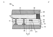
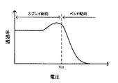
本発明の液晶装置に係る実施形態について、図1乃至図7を参照して説明する。
次に、本実施形態に係る液晶装置における配向維持部材の変形例について、図8を参照して説明する。ここに、図8は、本実施形態に係る配向維持部材の変形例を示す平面図である。
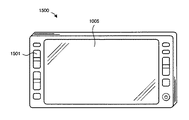
本発明に係る電子機器の実施形態について、図9を参照して説明する。ここに、図9は、上述した液晶装置100が適用されたカーナビゲーション装置の斜視図である。
Claims (7)
- 電圧無印加時における配向状態がスプレイ配向である液晶分子を含んでなる液晶層を挟持する一対の基板と、
前記一対の基板の一方の基板上における画素領域の周囲を規定する額縁領域に少なくとも部分的に配置される導電性の配向維持部材と、
前記一方の基板に配置される画素電極と、
前記一対の基板の他方の基板に前記画素電極と対応して配置される対向電極と、
を備え、
前記配向維持部材は、前記画素領域の外縁のうち相対向する二辺に沿って配置された本体部と、前記外縁のうち前記二辺の少なくとも一方に相隣接する辺に沿い、前記本体部が配置された第1層とは異なる第2層に配置された延設部とを有し、
前記配向維持部材と前記対向電極との間に、前記額縁領域のうち前記画素領域と隣接する領域の少なくとも一部における前記液晶層をベンド配向状態とするための電圧が駆動時に印加される、
ことを特徴とする液晶装置。 - 電位を、前記配向維持部材に供給する電圧供給手段を更に備えることを特徴とする請求項1に記載の液晶装置。
- 前記電圧供給手段は、前記画素領域における前記液晶層を駆動するための各種駆動用信号の一部と共用で、前記電位を供給することを特徴とする請求項2に記載の液晶装置。
- 前記配向維持部材は、静電気から当該液晶装置を保護する静電気保護回路の少なくとも一部を構成することを特徴とする請求項1乃至3のいずれか一項に記載の液晶装置。
- 前記配向維持部材は、前記一方の基板上で平面的に見て、島状に形成されていることを特徴とする請求項1乃至4のいずれか一項に記載の液晶装置。
- 前記一方の基板は、前記画素領域にマトリクス状に配列された複数の画素電極を有し、
前記配向維持部材は、前記複数の画素電極と層間絶縁膜を介して互いに異なる層に配置されている、
ことを特徴とする請求項1乃至5のいずれか一項に記載の液晶装置。 - 請求項1乃至6のいずれか一項に記載の液晶装置を備える電子機器。
Priority Applications (3)
| Application Number | Priority Date | Filing Date | Title |
|---|---|---|---|
| JP2008103428A JP4631923B2 (ja) | 2008-04-11 | 2008-04-11 | 液晶装置及び電子機器 |
| US12/404,680 US8081264B2 (en) | 2008-04-11 | 2009-03-16 | Liquid crystal device and electronic apparatus |
| CN2009101335105A CN101556420B (zh) | 2008-04-11 | 2009-04-08 | 液晶装置以及电子设备 |
Applications Claiming Priority (1)
| Application Number | Priority Date | Filing Date | Title |
|---|---|---|---|
| JP2008103428A JP4631923B2 (ja) | 2008-04-11 | 2008-04-11 | 液晶装置及び電子機器 |
Publications (2)
| Publication Number | Publication Date |
|---|---|
| JP2009251576A JP2009251576A (ja) | 2009-10-29 |
| JP4631923B2 true JP4631923B2 (ja) | 2011-02-16 |
Family
ID=41163692
Family Applications (1)
| Application Number | Title | Priority Date | Filing Date |
|---|---|---|---|
| JP2008103428A Active JP4631923B2 (ja) | 2008-04-11 | 2008-04-11 | 液晶装置及び電子機器 |
Country Status (3)
| Country | Link |
|---|---|
| US (1) | US8081264B2 (ja) |
| JP (1) | JP4631923B2 (ja) |
| CN (1) | CN101556420B (ja) |
Families Citing this family (1)
| Publication number | Priority date | Publication date | Assignee | Title |
|---|---|---|---|---|
| US20130140073A1 (en) * | 2011-12-01 | 2013-06-06 | Cn Innovations Limited | Routing structure for connecting sensor electrodes using black artwork on touch-panel glass |
Family Cites Families (7)
| Publication number | Priority date | Publication date | Assignee | Title |
|---|---|---|---|---|
| CN1179237C (zh) * | 1998-08-31 | 2004-12-08 | 精工爱普生株式会社 | 液晶屏及其制造方法 |
| CN1773333A (zh) * | 1998-09-03 | 2006-05-17 | 松下电器产业株式会社 | 液晶显示装置、其制造方法及其驱动方法 |
| JP4248160B2 (ja) * | 2001-04-16 | 2009-04-02 | 東芝松下ディスプレイテクノロジー株式会社 | 液晶表示素子とその製造方法 |
| JP2006201312A (ja) * | 2005-01-18 | 2006-08-03 | Nec Corp | 液晶表示パネル及び液晶表示装置 |
| JP4802023B2 (ja) | 2006-03-24 | 2011-10-26 | 東芝モバイルディスプレイ株式会社 | 液晶表示装置 |
| JP4305485B2 (ja) * | 2006-09-26 | 2009-07-29 | セイコーエプソン株式会社 | 液晶装置、液晶装置の駆動方法、プロジェクタ及び電子機器 |
| US7894007B2 (en) * | 2007-05-08 | 2011-02-22 | Toshiba Matsushita Display Technology Co., Ltd. | Liquid crystal display device |
-
2008
- 2008-04-11 JP JP2008103428A patent/JP4631923B2/ja active Active
-
2009
- 2009-03-16 US US12/404,680 patent/US8081264B2/en active Active
- 2009-04-08 CN CN2009101335105A patent/CN101556420B/zh active Active
Also Published As
| Publication number | Publication date |
|---|---|
| JP2009251576A (ja) | 2009-10-29 |
| CN101556420B (zh) | 2011-11-16 |
| CN101556420A (zh) | 2009-10-14 |
| US20090256982A1 (en) | 2009-10-15 |
| US8081264B2 (en) | 2011-12-20 |
Similar Documents
| Publication | Publication Date | Title |
|---|---|---|
| JP5217752B2 (ja) | 電気光学装置及び電子機器 | |
| US8194217B2 (en) | Electro-optical apparatus and electronic device having particular pixel configuration | |
| JP5024110B2 (ja) | 電気光学装置及び電子機器 | |
| JP5239512B2 (ja) | 電気光学装置及び電子機器 | |
| US8247818B2 (en) | Electro-optical device and electronic apparatus | |
| JP5396905B2 (ja) | 電気光学装置及び電子機器 | |
| JP2010048918A (ja) | 電気光学装置及び電子機器 | |
| JP2010210734A (ja) | 液晶装置及び電子機器 | |
| JP5200720B2 (ja) | 電気光学装置及び電子機器、並びに電気光学装置の製造方法 | |
| JP2011186285A (ja) | 電気光学装置及びその製造方法、並びに電子機器 | |
| JP4631923B2 (ja) | 液晶装置及び電子機器 | |
| JP5532944B2 (ja) | 電気光学装置用基板、電気光学装置及び電子機器 | |
| JP5182138B2 (ja) | 電気光学装置及び電子機器 | |
| JP5286782B2 (ja) | 電気光学装置用基板及び電気光学装置、並びに電子機器 | |
| JP5104156B2 (ja) | 電気光学装置及びこれを備えた電子機器 | |
| JP2010060901A (ja) | 電気光学装置及び電子機器 | |
| JP5499622B2 (ja) | 電気光学装置及び電子機器 | |
| JP2010039209A (ja) | 電気光学装置及びその製造方法並びに電子機器 | |
| JP5050891B2 (ja) | 電気光学装置及び電子機器 | |
| JP2008026771A (ja) | 電気光学装置及び電子機器 | |
| JP2006343529A (ja) | 液晶表示装置および液晶パネル | |
| JP2008145558A (ja) | 電気光学装置及び電子機器 | |
| JP2008145557A (ja) | 電気光学装置及び電子機器 | |
| JP2011170007A (ja) | 電気光学装置及び電子機器 | |
| JP2010191037A (ja) | 電気光学装置及び電子機器 |
Legal Events
| Date | Code | Title | Description |
|---|---|---|---|
| A977 | Report on retrieval |
Free format text: JAPANESE INTERMEDIATE CODE: A971007 Effective date: 20091228 |
|
| A131 | Notification of reasons for refusal |
Free format text: JAPANESE INTERMEDIATE CODE: A131 Effective date: 20100112 |
|
| A521 | Request for written amendment filed |
Free format text: JAPANESE INTERMEDIATE CODE: A523 Effective date: 20100218 |
|
| A131 | Notification of reasons for refusal |
Free format text: JAPANESE INTERMEDIATE CODE: A131 Effective date: 20100525 |
|
| A711 | Notification of change in applicant |
Free format text: JAPANESE INTERMEDIATE CODE: A711 Effective date: 20100526 |
|
| RD02 | Notification of acceptance of power of attorney |
Free format text: JAPANESE INTERMEDIATE CODE: A7422 Effective date: 20100526 |
|
| A521 | Request for written amendment filed |
Free format text: JAPANESE INTERMEDIATE CODE: A523 Effective date: 20100722 |
|
| TRDD | Decision of grant or rejection written | ||
| A01 | Written decision to grant a patent or to grant a registration (utility model) |
Free format text: JAPANESE INTERMEDIATE CODE: A01 Effective date: 20101019 |
|
| A01 | Written decision to grant a patent or to grant a registration (utility model) |
Free format text: JAPANESE INTERMEDIATE CODE: A01 |
|
| A61 | First payment of annual fees (during grant procedure) |
Free format text: JAPANESE INTERMEDIATE CODE: A61 Effective date: 20101101 |
|
| R151 | Written notification of patent or utility model registration |
Ref document number: 4631923 Country of ref document: JP Free format text: JAPANESE INTERMEDIATE CODE: R151 |
|
| FPAY | Renewal fee payment (event date is renewal date of database) |
Free format text: PAYMENT UNTIL: 20131126 Year of fee payment: 3 |
|
| FPAY | Renewal fee payment (event date is renewal date of database) |
Free format text: PAYMENT UNTIL: 20131126 Year of fee payment: 3 |
|
| S111 | Request for change of ownership or part of ownership |
Free format text: JAPANESE INTERMEDIATE CODE: R313113 |
|
| FPAY | Renewal fee payment (event date is renewal date of database) |
Free format text: PAYMENT UNTIL: 20131126 Year of fee payment: 3 |
|
| R350 | Written notification of registration of transfer |
Free format text: JAPANESE INTERMEDIATE CODE: R350 |
|
| R250 | Receipt of annual fees |
Free format text: JAPANESE INTERMEDIATE CODE: R250 |
|
| R250 | Receipt of annual fees |
Free format text: JAPANESE INTERMEDIATE CODE: R250 |
|
| R250 | Receipt of annual fees |
Free format text: JAPANESE INTERMEDIATE CODE: R250 |
|
| R250 | Receipt of annual fees |
Free format text: JAPANESE INTERMEDIATE CODE: R250 |
|
| R250 | Receipt of annual fees |
Free format text: JAPANESE INTERMEDIATE CODE: R250 |
|
| R250 | Receipt of annual fees |
Free format text: JAPANESE INTERMEDIATE CODE: R250 |
|
| R250 | Receipt of annual fees |
Free format text: JAPANESE INTERMEDIATE CODE: R250 |
|
| R250 | Receipt of annual fees |
Free format text: JAPANESE INTERMEDIATE CODE: R250 |
|
| S111 | Request for change of ownership or part of ownership |
Free format text: JAPANESE INTERMEDIATE CODE: R313111 |
|
| R350 | Written notification of registration of transfer |
Free format text: JAPANESE INTERMEDIATE CODE: R350 |
|
| R250 | Receipt of annual fees |
Free format text: JAPANESE INTERMEDIATE CODE: R250 |
|
| R250 | Receipt of annual fees |
Free format text: JAPANESE INTERMEDIATE CODE: R250 |
|
| R250 | Receipt of annual fees |
Free format text: JAPANESE INTERMEDIATE CODE: R250 |
|
| R250 | Receipt of annual fees |
Free format text: JAPANESE INTERMEDIATE CODE: R250 |
|
| S111 | Request for change of ownership or part of ownership |
Free format text: JAPANESE INTERMEDIATE CODE: R313113 |
|
| R350 | Written notification of registration of transfer |
Free format text: JAPANESE INTERMEDIATE CODE: R350 |
|
| R250 | Receipt of annual fees |
Free format text: JAPANESE INTERMEDIATE CODE: R250 |