JP4646743B2 - 半導体装置の製造方法 - Google Patents
半導体装置の製造方法 Download PDFInfo
- Publication number
- JP4646743B2 JP4646743B2 JP2005250694A JP2005250694A JP4646743B2 JP 4646743 B2 JP4646743 B2 JP 4646743B2 JP 2005250694 A JP2005250694 A JP 2005250694A JP 2005250694 A JP2005250694 A JP 2005250694A JP 4646743 B2 JP4646743 B2 JP 4646743B2
- Authority
- JP
- Japan
- Prior art keywords
- groove
- film
- oxide film
- thermal oxide
- semiconductor device
- Prior art date
- Legal status (The legal status is an assumption and is not a legal conclusion. Google has not performed a legal analysis and makes no representation as to the accuracy of the status listed.)
- Expired - Fee Related
Links
Images




Classifications
-
- H—ELECTRICITY
- H10—SEMICONDUCTOR DEVICES; ELECTRIC SOLID-STATE DEVICES NOT OTHERWISE PROVIDED FOR
- H10W—GENERIC PACKAGES, INTERCONNECTIONS, CONNECTORS OR OTHER CONSTRUCTIONAL DETAILS OF DEVICES COVERED BY CLASS H10
- H10W10/00—Isolation regions in semiconductor bodies between components of integrated devices
- H10W10/01—Manufacture or treatment
- H10W10/011—Manufacture or treatment of isolation regions comprising dielectric materials
- H10W10/014—Manufacture or treatment of isolation regions comprising dielectric materials using trench refilling with dielectric materials, e.g. shallow trench isolations
- H10W10/0145—Manufacture or treatment of isolation regions comprising dielectric materials using trench refilling with dielectric materials, e.g. shallow trench isolations of trenches having shapes other than rectangular or V-shape
-
- H—ELECTRICITY
- H10—SEMICONDUCTOR DEVICES; ELECTRIC SOLID-STATE DEVICES NOT OTHERWISE PROVIDED FOR
- H10W—GENERIC PACKAGES, INTERCONNECTIONS, CONNECTORS OR OTHER CONSTRUCTIONAL DETAILS OF DEVICES COVERED BY CLASS H10
- H10W10/00—Isolation regions in semiconductor bodies between components of integrated devices
- H10W10/10—Isolation regions comprising dielectric materials
- H10W10/17—Isolation regions comprising dielectric materials formed using trench refilling with dielectric materials, e.g. shallow trench isolations
Landscapes
- Element Separation (AREA)
- Bipolar Transistors (AREA)
Description
め込み層102の不純物拡散を抑制しようとすると、特にSTI溝の角部が十分な丸み形状とはならず、欠陥の発生を除去できない。また深い溝の凹部内面に絶縁膜を形成する際には、STI溝の角部は絶縁膜などで覆われているためストレスが開放されにくく、深い溝の凹部内面に絶縁膜を形成することに起因してストレスが蓄積されSTI溝の角部に欠陥が発生しやすくなる。
溝及び前記第2の溝の各角部が丸みを持ち、且つ前記第1の熱酸化膜の膜厚と比べて前記第2の熱酸化膜の膜厚が薄いことを特徴とする。
。
0が形成される。また、この深い溝70の形成時のエッチングによって、HTO膜8の厚みが薄くなる。この深い溝70は、N型エピタキシャルシリコン層3の上面から約6μmの深さを有するように形成する。このようにして、STI溝60よりも深い溝70を形成される。

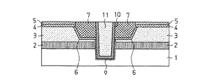
2 N+ 埋め込み層(第1の層)
3 エピタキシャル層(第2の層)
4 シリコン酸化膜
5 シリコン窒化膜
6 熱酸化膜(第1の熱酸化膜)
7 HDP−NSG膜(第1の埋め込み膜)
9 熱酸化膜(第2の熱酸化膜)
10 シリコン酸化膜
11 ポリシリコン膜(第2の埋め込み膜)
12 シリコン酸化膜
13 トレンチキャップ層
50 素子形成領域
14 ベース電極
15 シリコン酸化膜
16 エミッタ電極
60 STI溝(第1の溝)
61a、61b 第1の溝の角部
70 深い溝(第2の溝)
71a、71b 第2の溝の角部
Claims (3)
- 半導体基板上に、不純物を含む第1の層を形成する第1の工程と、
前記第1の層上に、第2の層を形成する第2の工程と、
前記第2の層に、第1の溝を形成する第3の工程と、
前記第1の溝の内面に、第1の熱酸化法により第1の熱酸化膜を形成する第4の工程と、
前記第1の溝に、第1の埋め込み膜を形成する第5の工程と、
前記第1の溝内に、前記第1の溝よりも深さの深い第2の溝を形成する第6の工程と、
前記第2の溝の内面に、前記第1の熱酸化法と同じ第2の熱酸化法により第2の熱酸化膜を形成する第7の工程と、
前記第2の溝に、第2の埋め込み膜を形成する第8の工程と、を備え、
前記第4の工程は、前記第1の溝の角部に丸みを形成する工程であり、前記第7の工程は、前記第2の溝の角部に丸みを形成する工程であって、且つ前記第1の熱酸化膜の膜厚と比べて、前記第2の熱酸化膜の膜厚を薄く形成することを特徴とした半導体装置の製造方法。 - 前記第6の工程における前記第2の溝の深さは、前記半導体基板に到達する深さであることを特徴とした請求項1に記載の半導体装置の製造方法。
- 前記第1の熱酸化膜の膜厚と前記第2の熱酸化膜の膜厚との膜厚差が6nm以上となるように形成することを特徴とした請求項1または2に記載の半導体装置の製造方法。
Priority Applications (3)
| Application Number | Priority Date | Filing Date | Title |
|---|---|---|---|
| JP2005250694A JP4646743B2 (ja) | 2004-09-08 | 2005-08-31 | 半導体装置の製造方法 |
| US11/220,420 US7405461B2 (en) | 2004-09-08 | 2005-09-07 | Semiconductor device and method for manufacturing semiconductor device |
| US12/071,199 US7638409B2 (en) | 2004-09-08 | 2008-02-19 | Semiconductor device and method for manufacturing semiconductor device |
Applications Claiming Priority (2)
| Application Number | Priority Date | Filing Date | Title |
|---|---|---|---|
| JP2004261389 | 2004-09-08 | ||
| JP2005250694A JP4646743B2 (ja) | 2004-09-08 | 2005-08-31 | 半導体装置の製造方法 |
Publications (2)
| Publication Number | Publication Date |
|---|---|
| JP2006108646A JP2006108646A (ja) | 2006-04-20 |
| JP4646743B2 true JP4646743B2 (ja) | 2011-03-09 |
Family
ID=35996803
Family Applications (1)
| Application Number | Title | Priority Date | Filing Date |
|---|---|---|---|
| JP2005250694A Expired - Fee Related JP4646743B2 (ja) | 2004-09-08 | 2005-08-31 | 半導体装置の製造方法 |
Country Status (2)
| Country | Link |
|---|---|
| US (2) | US7405461B2 (ja) |
| JP (1) | JP4646743B2 (ja) |
Families Citing this family (11)
| Publication number | Priority date | Publication date | Assignee | Title |
|---|---|---|---|---|
| US7435661B2 (en) * | 2006-01-27 | 2008-10-14 | Atmel Corporation | Polish stop and sealing layer for manufacture of semiconductor devices with deep trench isolation |
| US7820519B2 (en) * | 2006-11-03 | 2010-10-26 | Freescale Semiconductor, Inc. | Process of forming an electronic device including a conductive structure extending through a buried insulating layer |
| US8188543B2 (en) * | 2006-11-03 | 2012-05-29 | Freescale Semiconductor, Inc. | Electronic device including a conductive structure extending through a buried insulating layer |
| EP2036517A1 (de) * | 2007-09-17 | 2009-03-18 | WALDEMAR LINK GmbH & Co. KG | Endoprothesenkomponente |
| US7998808B2 (en) * | 2008-03-21 | 2011-08-16 | International Rectifier Corporation | Semiconductor device fabrication using spacers |
| US8211778B2 (en) * | 2008-12-23 | 2012-07-03 | Micron Technology, Inc. | Forming isolation regions for integrated circuits |
| JP5010660B2 (ja) * | 2009-09-25 | 2012-08-29 | 株式会社東芝 | 半導体装置およびその製造方法 |
| JP6103894B2 (ja) * | 2012-11-20 | 2017-03-29 | ギガフォトン株式会社 | ターゲット供給装置 |
| US9337078B2 (en) * | 2013-09-11 | 2016-05-10 | Globalfoundries Inc. | Heat dissipation through device isolation |
| KR102335490B1 (ko) * | 2017-12-14 | 2021-12-03 | 현대자동차 주식회사 | 반도체 소자 및 그 제조 방법 |
| US10879106B2 (en) * | 2018-02-21 | 2020-12-29 | Texas Instruments Incorporated | Apparatus with overlapping deep trench and shallow trench and method of fabricating the same with low defect density |
Family Cites Families (8)
| Publication number | Priority date | Publication date | Assignee | Title |
|---|---|---|---|---|
| JPS6122646A (ja) * | 1984-07-11 | 1986-01-31 | Hitachi Ltd | 絶縁分離溝の埋込み方法 |
| JPS63144540A (ja) * | 1986-12-09 | 1988-06-16 | Toshiba Corp | 半導体装置の製造方法 |
| US5943578A (en) * | 1993-02-05 | 1999-08-24 | Kabushiki Kaisha Toshiba | Method of manufacturing a semiconductor device having an element isolating region |
| JP3382063B2 (ja) * | 1995-06-14 | 2003-03-04 | 株式会社東芝 | 半導体装置の製造方法 |
| JP2955459B2 (ja) * | 1993-12-20 | 1999-10-04 | 株式会社東芝 | 半導体装置の製造方法 |
| US5837612A (en) * | 1997-08-01 | 1998-11-17 | Motorola, Inc. | Silicon chemical mechanical polish etch (CMP) stop for reduced trench fill erosion and method for formation |
| US20030017710A1 (en) * | 2001-07-19 | 2003-01-23 | Chartered Semiconductor Manufacturing Ltd. | Method to improve latchup by forming selective sloped staircase STI structure to use in the I/0 or latchup sensitive area |
| JP4592340B2 (ja) * | 2004-06-29 | 2010-12-01 | 三洋電機株式会社 | 半導体装置の製造方法 |
-
2005
- 2005-08-31 JP JP2005250694A patent/JP4646743B2/ja not_active Expired - Fee Related
- 2005-09-07 US US11/220,420 patent/US7405461B2/en not_active Expired - Fee Related
-
2008
- 2008-02-19 US US12/071,199 patent/US7638409B2/en not_active Expired - Lifetime
Also Published As
| Publication number | Publication date |
|---|---|
| US7638409B2 (en) | 2009-12-29 |
| US7405461B2 (en) | 2008-07-29 |
| US20060051932A1 (en) | 2006-03-09 |
| JP2006108646A (ja) | 2006-04-20 |
| US20080153254A1 (en) | 2008-06-26 |
Similar Documents
| Publication | Publication Date | Title |
|---|---|---|
| CN1208823C (zh) | 浅沟隔离半导体及其制造 | |
| US7638409B2 (en) | Semiconductor device and method for manufacturing semiconductor device | |
| JP2009021569A (ja) | Sti構造を有する半導体素子及びその製造方法 | |
| JPH11340313A (ja) | トレンチ隔離形成方法 | |
| JP2005203508A (ja) | 半導体装置の製造方法 | |
| KR100346295B1 (ko) | 서브-마이크론 깊이의 디바이스 공정용 변형 리세스 locos분리 공정 | |
| CN100376025C (zh) | 半导体装置的制造方法 | |
| US20090191688A1 (en) | Shallow Trench Isolation Process Using Two Liners | |
| JP2003017555A (ja) | 半導体集積回路装置およびその製造方法 | |
| JP2005322872A (ja) | トレンチ型素子分離膜を備えた半導体素子の製造方法 | |
| JPH10303291A (ja) | 半導体装置及びその製造方法 | |
| US20030209760A1 (en) | Semiconductor integrated circuit and method of fabricating the same | |
| CN119480637A (zh) | 一种半导体结构的制备方法 | |
| US5851901A (en) | Method of manufacturing an isolation region of a semiconductor device with advanced planarization | |
| JP2008010724A (ja) | 半導体装置及びその製造方法 | |
| CN1937252A (zh) | 制造半导体器件的方法 | |
| JP4592193B2 (ja) | 半導体装置の製造方法 | |
| KR100561515B1 (ko) | 반도체 소자의 소자분리막 형성 방법 | |
| JP2004152851A (ja) | 半導体装置の製造方法 | |
| JP4416527B2 (ja) | 半導体装置の製造方法 | |
| KR100801733B1 (ko) | 서로 다른 두께의 측벽산화막을 갖는 트랜치 소자분리막형성방법 | |
| JP3744889B2 (ja) | 半導体装置の製造方法 | |
| JP4549039B2 (ja) | 半導体集積回路の製造方法 | |
| JP2009177063A (ja) | 半導体装置の製造方法および半導体装置 | |
| KR100552852B1 (ko) | 얕은 트렌치 소자 분리 제조 방법 |
Legal Events
| Date | Code | Title | Description |
|---|---|---|---|
| A621 | Written request for application examination |
Free format text: JAPANESE INTERMEDIATE CODE: A621 Effective date: 20061109 |
|
| A977 | Report on retrieval |
Free format text: JAPANESE INTERMEDIATE CODE: A971007 Effective date: 20091127 |
|
| A131 | Notification of reasons for refusal |
Free format text: JAPANESE INTERMEDIATE CODE: A131 Effective date: 20091208 |
|
| A521 | Request for written amendment filed |
Free format text: JAPANESE INTERMEDIATE CODE: A523 Effective date: 20100208 |
|
| TRDD | Decision of grant or rejection written | ||
| A01 | Written decision to grant a patent or to grant a registration (utility model) |
Free format text: JAPANESE INTERMEDIATE CODE: A01 Effective date: 20101109 |
|
| A01 | Written decision to grant a patent or to grant a registration (utility model) |
Free format text: JAPANESE INTERMEDIATE CODE: A01 |
|
| A61 | First payment of annual fees (during grant procedure) |
Free format text: JAPANESE INTERMEDIATE CODE: A61 Effective date: 20101207 |
|
| FPAY | Renewal fee payment (event date is renewal date of database) |
Free format text: PAYMENT UNTIL: 20131217 Year of fee payment: 3 |
|
| FPAY | Renewal fee payment (event date is renewal date of database) |
Free format text: PAYMENT UNTIL: 20131217 Year of fee payment: 3 |
|
| FPAY | Renewal fee payment (event date is renewal date of database) |
Free format text: PAYMENT UNTIL: 20131217 Year of fee payment: 3 |
|
| S111 | Request for change of ownership or part of ownership |
Free format text: JAPANESE INTERMEDIATE CODE: R313113 |
|
| FPAY | Renewal fee payment (event date is renewal date of database) |
Free format text: PAYMENT UNTIL: 20131217 Year of fee payment: 3 |
|
| R360 | Written notification for declining of transfer of rights |
Free format text: JAPANESE INTERMEDIATE CODE: R360 |
|
| FPAY | Renewal fee payment (event date is renewal date of database) |
Free format text: PAYMENT UNTIL: 20131217 Year of fee payment: 3 |
|
| R370 | Written measure of declining of transfer procedure |
Free format text: JAPANESE INTERMEDIATE CODE: R370 |
|
| R250 | Receipt of annual fees |
Free format text: JAPANESE INTERMEDIATE CODE: R250 |
|
| LAPS | Cancellation because of no payment of annual fees |