JP4686830B2 - Solid-state imaging device and driving method thereof - Google Patents
Solid-state imaging device and driving method thereof Download PDFInfo
- Publication number
- JP4686830B2 JP4686830B2 JP2000257463A JP2000257463A JP4686830B2 JP 4686830 B2 JP4686830 B2 JP 4686830B2 JP 2000257463 A JP2000257463 A JP 2000257463A JP 2000257463 A JP2000257463 A JP 2000257463A JP 4686830 B2 JP4686830 B2 JP 4686830B2
- Authority
- JP
- Japan
- Prior art keywords
- gate
- overflow
- electrode
- transfer
- layer
- Prior art date
- Legal status (The legal status is an assumption and is not a legal conclusion. Google has not performed a legal analysis and makes no representation as to the accuracy of the status listed.)
- Expired - Fee Related
Links
Images


Classifications
-
- H—ELECTRICITY
- H10—SEMICONDUCTOR DEVICES; ELECTRIC SOLID-STATE DEVICES NOT OTHERWISE PROVIDED FOR
- H10F—INORGANIC SEMICONDUCTOR DEVICES SENSITIVE TO INFRARED RADIATION, LIGHT, ELECTROMAGNETIC RADIATION OF SHORTER WAVELENGTH OR CORPUSCULAR RADIATION
- H10F39/00—Integrated devices, or assemblies of multiple devices, comprising at least one element covered by group H10F30/00, e.g. radiation detectors comprising photodiode arrays
- H10F39/10—Integrated devices
- H10F39/12—Image sensors
- H10F39/18—Complementary metal-oxide-semiconductor [CMOS] image sensors; Photodiode array image sensors
- H10F39/186—Complementary metal-oxide-semiconductor [CMOS] image sensors; Photodiode array image sensors having arrangements for blooming suppression
- H10F39/1865—Overflow drain structures
Landscapes
- Solid State Image Pick-Up Elements (AREA)
- Transforming Light Signals Into Electric Signals (AREA)
Description
【0001】
【発明の属する技術分野】
本発明は、転送レジスタに対してオーバーフロードレインが設けられた固体撮像素子及びその駆動方法に係わる。
【0002】
【従来の技術】
従来、CCD固体撮像素子の転送レジスタにおいてオーバーフロー制御を行う場合には、転送レジスタのストレージ電極を形成する下層の多結晶シリコン層の横に上層の多結晶シリコン層とバリア用インプラによって、オーバーフローバリアを形成していた。
【0003】
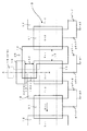
この従来のオーバーフロー制御を行う構造の概略構成図(平面図)を図5に示す。
転送レジスタ50の上に、第1層の転送電極51と第2層の転送電極52とが交互に配置されている。
第1層の転送電極51はストレージ電極St1,St2となり、第2層の転送電極52はトランスファー電極Tr1,Tr2となる。
ストレージ電極St1及びトランスファー電極Tr1には、それぞれの駆動パルスφSt1,φTr1として第1相の駆動パルスφ1が印加される。
ストレージ電極St2及びトランスファー電極Tr2には、それぞれの駆動パルスφSt2,φTr2として第2相の駆動パルスφ2が印加される。
【0004】
そして、図5のほぼ中央の第1相のストレージ電極St1の側方に、オーバーフローコントロールゲートOFCG及びオーバーフロードレインOFDが設けられている。
【0005】
また、図5のY−Y´における断面図を図6に示す。
オーバーフローコントロールゲートOFCGは、図5及び図6に示すように、ゲート電極54とN- 領域56とから構成されている。
ゲート電極54は、トランスファー電極Tr1,Tr2を構成する第2層の転送電極52と同じ第2層の多結晶シリコン層により形成されている。このゲート電極54には、駆動パルスφOFCGが印加される。
N- 領域56は、半導体基板1のP型ウエル領域2内に、N型不純物をイオン注入して形成されている。
オーバーフロードレインOFDは、半導体基板1のP型ウエル領域2内に高濃度N型不純物をイオン注入して形成されたN++領域55により構成される。
尚、図中3は、ストレージ電極St1,St2の下に形成されたN+ 領域を示し、この領域3に転送中の電荷が蓄積される。
【0006】
さらに、図5のY−Y´におけるポテンシャル断面図を図7に示す。
図7に示すように、ゲート電極54及びN- 領域56によるオーバーフローコントロールゲートOFCGがバリアとなっており、このバリアを越えた電荷をオーバーフロードレインOFDに捨てている。
【0007】
この構成において、オーバーフローコントロールゲートOFCGのバリアの高さに影響する因子としては、オーバーフローコントロールゲートOFCGのゲート電極54の第1相のストレージ電極St1と重なっていない部分の長さL1即ちオーバーフローコントロールゲートOFCGの実効長と、N- 領域56の不純物濃度とが挙げられる。
【0008】
また、図5の構成における駆動パルスのタイミングチャートを図8に示す。
第1相のストレージ電極St1の駆動パルスφSt1及び第1相のトランスファー電極Tr1の駆動パルスφTr1は、共に同じ駆動パルス(第1相の駆動パルスφ1)が印加される。
一方、第2相のストレージ電極St2の駆動パルスφSt2及び第2相のトランスファー電極Tr2の駆動パルスφTr2は、共に同じ駆動パルス(第2相の駆動パルスφ2)が印加される。
第1相の駆動パルスφ1と第2相の駆動パルスφ2とは互いに逆相である。
【0009】
そして、オーバーフローコントロールゲートOFCGの駆動パルスφOFCGは、第1相の駆動パルスφ1と同相の駆動パルスとなっている。
【0010】
これにより、次のように電荷の転送及びオーバーフローの動作がなされる。
第1相の駆動パルスφ1がハイレベルHiで第1相のストレージ電極St1に電荷があるときには、オーバーフローコントロールゲートOFCGの駆動パルスφOFCGもハイレベルHiであり、オーバーフローバリアの高さが低くなり所定量でオーバーフローさせることが可能になる。
一方、第1相の駆動パルスφ1がローレベルLoで第1相のストレージ電極St1から隣の第2相の電極Tr2,St2へ電荷が転送されるときには、オーバーフローコントロールゲートOFCGの駆動パルスφOFCGもローレベルLoであり、オーバーフローバリアの高さが高くなって、転送中の電荷がバリアを越えないようにすることができる。
【0011】
【発明が解決しようとする課題】
しかしながら、この従来の構成の場合、下層の第1層の多結晶シリコン層から成る第1相のストレージ電極St1と、上層の第2層の多結晶シリコン層から成るオーバーフローコントロールOFCGゲートのゲート電極54との間に合わせずれが生じると、オーバーフローコントロールゲートOFCGの実効長L1が変化してしまう。
この実効長L1が変化するとオーバーフローコントロールゲートOFCGによるバリアの高さも変化してしまう。また、転送チャネル50のバリアの高さを規定するトランスファー電極Tr1の実効長Lとの関係も変化する。
【0012】
また、N- 領域56とゲート電極54との合わせズレや、下層の多結晶シリコン層51や上層の多結晶シリコン層52,54の線幅のばらつき等によっても、オーバーフローコントロールゲートOFCGによるバリアの高さが変化する。
【0013】
そして、合わせズレ等のばらつきが大きいと、オーバーフローコントロールゲートOFCGのバリア高さとトランスファー電極Tr1のバリア高さの差が、小さくなったり大きくなり過ぎたりして、適切なオーバーフロー制御ができない場合があった。
このことが、細かな制御を行う場合や固体撮像素子を微細化する際に問題となっていた。
【0014】
上述した問題の解決のために、本発明においては、適切なオーバーフロー制御を行うことができる固体撮像素子及びその駆動方法を提供するものである。
【0015】
【課題を解決するための手段】
本発明の固体撮像素子は、転送レジスタにオーバーフローコントロールゲート及びオーバーフロードレインが設けられ、転送レジスタにおいては、第1層の転送電極と第2層の転送電極とが交互に配置され、オーバーフローコントロールゲートは、ゲート電極と、このゲート電極の下のN − 領域とにより構成され、オーバーフロードレインは、N ++ 領域により構成され、オーバーフローコントロールゲートのゲート電極が、転送レジスタの第2層の転送電極と一体化して形成され、オーバーフローコントロールゲートとオーバーフロードレインとの間にゲートが設けられ、このゲートは第1層の転送電極と同じ層により形成され、このゲートの下にN + 領域が形成され、オーバーフローコントロールゲートのゲート電極が転送レジスタ側及びオーバーフロードレイン側においてそれぞれ下層の第1層の転送電極上及びゲート上に重ねて形成されているものである。
本発明の固体撮像素子の駆動方法は、転送レジスタにオーバーフローコントロールゲート及びオーバーフロードレインが設けられ、転送レジスタにおいては、第1層の転送電極と第2層の転送電極とが交互に配置され、オーバーフローコントロールゲートは、ゲート電極と、このゲート電極の下のN − 領域とにより構成され、オーバーフロードレインは、N ++ 領域により構成され、オーバーフローコントロールゲートのゲート電極が、転送レジスタの第2層の転送電極と一体化して形成され、オーバーフローコントロールゲートとオーバーフロードレインとの間にゲートが設けられ、このゲートは第1層の転送電極と同じ層により形成され、このゲートの下にN + 領域が形成され、オーバーフローコントロールゲートのゲート電極が、転送レジスタ側及びオーバーフロードレイン側においてそれぞれ下層の第1層の転送電極上及びゲート上に重ねて形成されている固体撮像素子に対して、オーバーフローコントロールゲートのゲート電極には、転送レジスタの電極に印加される駆動パルスを印加し、オーバーフロードレイン側のゲートには、常にオン状態とする駆動パルスを印加するものである。
【0016】
上述の本発明の固体撮像素子の構成によれば、オーバーフローコントロールゲートのゲート電極が転送レジスタ側及びオーバーフロードレイン側においてそれぞれ下層の第1層の転送電極上及びゲート上に重ねて形成されていることにより、オーバーフローコントロールゲートの実効長が、転送レジスタ側及びオーバーフロードレイン側の下層の第1層の転送電極及びゲートの間隔により規定される。
上述の本発明の固体撮像素子の駆動方法によれば、オーバーフローコントロールゲートのゲート電極には、転送レジスタの電極に印加される駆動パルスを印加し、オーバーフロードレイン側のゲートには、常にオン状態とする駆動パルスを印加することにより、オーバーフロードレイン側のゲートが常にオン状態となっていて、オーバーフローコントロールゲートによるバリアを超えた電荷を妨げることなくオーバーフロードレインに排出することができる。
【0017】
【発明の実施の形態】
本発明は、転送レジスタにオーバーフローコントロールゲート及びオーバーフロードレインが設けられ、転送レジスタにおいては、第1層の転送電極と第2層の転送電極とが交互に配置され、オーバーフローコントロールゲートは、ゲート電極と、このゲート電極の下のN − 領域とにより構成され、オーバーフロードレインは、N ++ 領域により構成され、オーバーフローコントロールゲートのゲート電極が、転送レジスタの第2層の転送電極と一体化して形成され、オーバーフローコントロールゲートとオーバーフロードレインとの間にゲートが設けられ、このゲートは第1層の転送電極と同じ層により形成され、このゲートの下にN + 領域が形成され、オーバーフローコントロールゲートのゲート電極が転送レジスタ側及びオーバーフロードレイン側においてそれぞれ下層の第1層の転送電極上及びゲート上に重ねて形成されている固体撮像素子である。
本発明は、転送レジスタにオーバーフローコントロールゲート及びオーバーフロードレインが設けられ、転送レジスタにおいては、第1層の転送電極と第2層の転送電極とが交互に配置され、オーバーフローコントロールゲートは、ゲート電極と、このゲート電極の下のN − 領域とにより構成され、オーバーフロードレインは、N ++ 領域により構成され、オーバーフローコントロールゲートのゲート電極が、転送レジスタの第2層の転送電極と一体化して形成され、オーバーフローコントロールゲートとオーバーフロードレインとの間にゲートが設けられ、このゲートは第1層の転送電極と同じ層により形成され、このゲートの下にN + 領域が形成され、オーバーフローコントロールゲートのゲート電極が、転送レジスタ側及びオーバーフロードレイン側においてそれぞれ下層の第1層の転送電極上及びゲート上に重ねて形成されている固体撮像素子に対して、オーバーフローコントロールゲートのゲート電極には、転送レジスタの電極に印加される駆動パルスを印加し、オーバーフロードレイン側のゲートには、常にオン状態とする駆動パルスを印加する固体撮像素子の駆動方法である。
【0018】
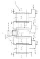
図1は本発明の一実施の形態として、CCD固体撮像素子の転送レジスタの要部の拡大平面図を示す。
転送レジスタ10の上に、第1層の転送電極11と第2層の転送電極12とが交互に配置されている。
第1層の転送電極11はストレージ電極St1,St2となり、第2層の転送電極12はトランスファー電極Tr1,Tr2となる。
ストレージ電極St1及びトランスファー電極Tr1には、それぞれの駆動パルスφSt1,φTr1として第1相の駆動パルスφ1が印加される。
ストレージ電極St2及びトランスファー電極Tr2には、それぞれの駆動パルスφSt2,φTr2として第2相の駆動パルスφ2が印加される。
【0019】
本実施の形態では、特に図1のほぼ中央の第1相のストレージ電極St1の側方に、オーバーフローコントロールゲートOFCG及びオーバーフロードレインOFDが設けられ、さらにこれらオーバーフローコントロールゲートOFCG及びオーバーフロードレインOFDの間にゲート13が設けられている。
【0020】
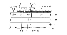
また、図1のA−A´における断面図を図2に示す。尚、図2において、半導体基板1、P型ウエル領域2、並びにストレージ電極St1,St2用のN+ 領域3は、図6と同様であるので同一符号を付している。
オーバーフローコントロールゲートOFCGは、図1及び図2に示すように、第1相のトランスファー電極Tr1を構成している第2層の転送電極12をL字状に延長した部分12Aから成るゲート電極とN- 領域14とから構成されている。
ゲート電極12Aが第1相のトランスファー電極Tr1と導通しているため、このゲート電極12Aには第1相のトランスファー電極Tr1の駆動パルスφTr1が印加される。
N- 領域14は、半導体基板1のP型ウエル領域2内に、N型不純物をイオン注入して形成されている。
オーバーフロードレインOFDは、半導体基板1のP型ウエル領域2内に高濃度N型不純物をイオン注入して形成されたN++領域15により構成される。
【0021】
また、オーバーフローコントロールゲートOFCG及びオーバーフロードレインOFDの間のゲート13は、第1相のストレージ電極St1と同じ第1層の多結晶シリコン層により形成される。
このゲート13には駆動パルスφGが印加される。
【0022】
そして、オーバーフローコントロールゲートOFCGのゲート電極12Aは、転送レジスタ10側において第1層の多結晶シリコン層によるストレージ電極St1上にある。この点は図5の構成と同様である。
さらに、オーバーフローコントロールゲートOFCGのゲート電極12Aは、オーバーフロードレインOFD側においても、第1層の多結晶シリコン層によるゲート13上にある。この点が図5の構成とは異なっている。
【0023】
これにより、それぞれ第1層の多結晶シリコン層により形成されるゲート13及び第1相のストレージ電極St1の間隔によって、その上の第2層の多結晶シリコン層により形成されるオーバーフローコントロールゲートOFCGの実効長L2が規定される。
【0024】
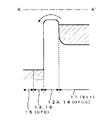
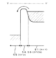
さらに、図1のA−A´におけるポテンシャル断面図を図3に示す。
図3に示すように、ゲート電極12A及びN- 領域14によるオーバーフローコントロールゲートOFCGがバリアとなっており、このバリアを越えた電荷をオーバーフロードレインOFDに捨てることができる。
【0025】
この構成において、オーバーフローバリアの高さに影響する因子としては、オーバーフローコントロールゲートOFCGのゲート電極12Aの下層の電極St1及び13と重なっていない部分の長さL2即ちオーバーフローコントロールゲートOFCGの実効長と、N- 領域14の不純物濃度とが挙げられる。
【0026】
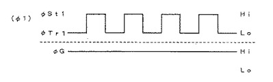
図1の構成における駆動パルスのタイミングチャートを図4に示す。
第1相のストレージ電極St1の駆動パルスφSt1及び第1相のトランスファー電極Tr1の駆動パルスφTr1は、共に同じ駆動パルス(第1相の駆動パルスφ1)が印加される。
そして、第1相のトランスファー電極Tr1と導通されたオーバーフローコントロールゲートOFCGのゲート電極12Aも、同じ駆動パルスφTr1(φ1)により動作する。
【0027】
また、ゲート電極13の駆動パルスφGは、常にハイレベルHiとされる。
従って、ゲート13は常にオン状態となっていて、オーバーフローコントロールゲートOFCGによるバリアを超えた電荷を妨げることなくオーバーフロードレインOFDに排出することができる。
尚、第2相の駆動パルスφ2は、図8と同様であるので、この図4では省略している。
【0028】
これにより、次のように電荷の転送及びオーバーフローの動作がなされる。
第1相の駆動パルスφ1がハイレベルHiであるときには、第1相のストレージ電極St1に電荷があり、かつオーバーフローコントロールゲートOFCGのゲート電極12AもハイレベルHiであり、オーバーフローバリアの高さが低くなり所定量でオーバーフローさせることが可能になる。
一方、第1相の駆動パルスφ1がローレベルLoであるときには、第1相のストレージ電極St1から隣の第2相の電極Tr2,St2へ電荷が転送され、オーバーフローコントロールゲートOFCGのゲート電極12AもローレベルLoであり、オーバーフローバリアの高さが高くなって、転送中の電荷がバリアを越えないようにすることができる。
【0029】
そして、オーバーフローコントロールゲートOFCGの実効長L2となる両側の第1層の電極St1,13の間隔L2を、第1相のトランスファー電極Tr1の実効長L3即ちストレージ電極St1,St2の間隔よりも狭くすることにより、トランスファー電極Tr1のバリア高さよりもオーバーフローコントロールゲートOFCGのバリア高さを低く設定することができる。
【0030】
本実施の形態の構成では、オーバーフローコントロールゲートOFCGのバリアの高さを規定する実効長L2のばらつき要因としては、両側の第1層の電極13,St1の間隔だけである。
そして、オーバーフローコントロールゲートOFCGも、トランスファー電極Tr1も、いずれも両側の第1層の電極の間隔及び不純物濃度でバリアの高さが設定される。
従って、オーバーフローコントロールゲートOFCGの両側の第1層の電極13及びSt1の間隔やN- 領域14の不純物濃度がばらついても、オーバーフローコントロールゲートOFCG及びトランスファー電極Tr1が等しくバリアが高くなる(低くなる)方向に動く。即ち例えば一方の間隔が狭くなったときは、他方の間隔も同様に狭くなる。
これにより、第1層の電極の間隔や不純物濃度にかかわらず、両者のバリアの関係が、ほぼ所定の差に保たれることになる。
【0031】
これにより、オーバーフローバリアの制御を非常に高い精度で行うことができる。
【0032】
上述の構成のオーバーフローコントロールゲートOFCG及びオーバーフロードレインOFDは、固体撮像素子において電荷転送を行う転送レジスタ10の途中に設ける。
例えばラインセンサでは、各転送レジスタにおいて、センサ(画素)のある部分と出力部との間の1カ所にオーバーフローコントロールゲートOFCG及びオーバーフロードレインOFDを設ける。尚、センサの両側で読み出して、出力部の手前で合流させる構成の場合には、合流する前に設けるようにする。
また、例えばエリアセンサでは、垂直転送レジスタから水平転送レジスタへの接続部や、水平転送レジスタの途中にオーバーフローコントロールゲートOFCG及びオーバーフロードレインOFDを設けることができる。
【0033】
上述の本実施の形態によれば、オーバーフローコントロールゲートOFCGの実効長L2が、両側の第1層の電極13,St1の間隔で規定されるので、オーバーフローコントロールゲートOFCGのバリア高さのばらつき要因を少なくすることができる。
そして、両側の第1層の電極13,St1の間隔がばらついても、トランスファー電極Tr1の実効長L3も連動して変化するため、オーバーフローコントロールゲートOFCGによるバリアの高さとトランスファー電極Tr1によるバリアの高さとの関係が所定の関係にほぼ保たれる。
【0034】
即ち本実施の形態の構成により、適切なオーバーフロー制御を行うことができる。
従って、細かい制御を行うことや、固体撮像素子の微細化を図ることが可能になる。
【0035】
また、上述の実施の形態では、オーバーフローコントロールゲートOFCGのゲート電極12Aと第1相のトランスファー電極Tr1とをL字状の一体化したパターンで形成しているため、コンタクト部を1つ設けるだけでオーバーフローコントロールゲートOFCG及びトランスファー電極Tr1を両方駆動させることが可能になる。
【0036】
従って、コンタクト部をそれぞれに設ける必要がなくなり、従来より電極の微細化を図ることが可能になる。そして、例えばL字の角部にコンタクト部を設ければ、コンタクト部オーバーフローコントロールゲートOFCG及びトランスファー電極Tr1の実効長L2及びL3をコンタクト部に係わらず自由に設定することが可能になる。
【0037】
尚、上述の実施の形態では、オーバーフローコントロールゲートOFCGのゲート電極12Aと第1相のトランスファー電極Tr1とを一体化したパターンで形成しているが、これらを図5の従来例のように別々に形成してもよい。この場合は、それぞれにコンタクト部を設けた上で、共に同じ第1相の駆動パルスφ1を印加するように構成する。
【0038】
上述の実施の形態は、2層2相駆動の場合であるが、3相や4相等他の駆動方式の転送レジスタに関しても同様に本発明を適用することができる。
そして、いずれの駆動方式の場合も、オーバーフローバリアの高さを下層の多結晶シリコン層の間隔によって規定することができる。
【0039】
本発明は、上述の実施の形態に限定されるものではなく、本発明の要旨を逸脱しない範囲でその他様々な構成が取り得る。
【0040】
【発明の効果】
上述の本発明によれば、オーバーフローコントロールゲートのバリア高さのばらつき要因を少なくすることができ、適切なオーバーフロー制御を行うことができる。
従って本発明により、細かい制御を行うことや、固体撮像素子の微細化を図ることが可能になる。
【図面の簡単な説明】
【図1】本発明の一実施の形態のCCD固体撮像素子の転送レジスタの要部の拡大平面図である。
【図2】図1のA−A´における断面図である。
【図3】図1のA−A´におけるポテンシャル断面図である。
【図4】図1の構成における駆動パルスのタイミングチャートである。
【図5】従来のCCD固体撮像素子の転送レジスタの要部の拡大平面図である。
【図6】図5のY−Y´における断面図である。
【図7】図5のY−Y´におけるポテンシャル断面図である。
【図8】図8の構成における駆動パルスのタイミングチャートである。
【符号の説明】
1 N型基板、2 P型ウエル領域、10 転送レジスタ、11 第1層の転送電極、12 第2層の転送電極、13 ゲート、OFCG オーバーフローコントロールゲート、OFD オーバーフロードレイン、St1,St2 ストレージ電極、Tr1,Tr2 トランスファー電極[0001]
BACKGROUND OF THE INVENTION
The present invention relates to a solid-state imaging device in which an overflow drain is provided for a transfer register and a driving method thereof .
[0002]
[Prior art]
Conventionally, when performing overflow control in a transfer register of a CCD solid-state imaging device, an overflow barrier is formed by an upper polycrystalline silicon layer and a barrier implant next to a lower polycrystalline silicon layer forming a storage electrode of the transfer register. Was forming.
[0003]
FIG. 5 shows a schematic configuration diagram (plan view) of a structure for performing this conventional overflow control.
On the
The first
The first-phase drive pulse φ1 is applied to the storage electrode St1 and the transfer electrode Tr1 as the drive pulses φSt1 and φTr1.
A second-phase drive pulse φ2 is applied to the storage electrode St2 and the transfer electrode Tr2 as the drive pulses φSt2 and φTr2.
[0004]
Then, an overflow control gate OFCG and an overflow drain OFD are provided on the side of the first-phase storage electrode St1 in the middle of FIG.
[0005]
Further, FIG. 6 shows a cross-sectional view taken along line YY ′ of FIG.
The overflow control gate OFCG is composed of a
The
The N − region 56 is formed by ion-implanting N-type impurities in the P-
The overflow drain OFD is composed of an N ++ region 55 formed by ion-implanting a high concentration N-type impurity into the P-
In the figure,
[0006]
Furthermore, FIG. 7 shows a potential cross-sectional view at YY ′ of FIG.
As shown in FIG. 7, the overflow control gate OFCG by the
[0007]
In this configuration, factors affecting the barrier height of the overflow control gate OFCG include the length L1 of the overflow control gate OFCG that does not overlap the first phase storage electrode St1 of the
[0008]
FIG. 8 shows a timing chart of drive pulses in the configuration of FIG.
The same drive pulse (first phase drive pulse φ1) is applied to both the drive pulse φSt1 of the first phase storage electrode St1 and the drive pulse φTr1 of the first phase transfer electrode Tr1.
On the other hand, the same drive pulse (second phase drive pulse φ2) is applied to the drive pulse φSt2 of the second phase storage electrode St2 and the drive pulse φTr2 of the second phase transfer electrode Tr2.
The first-phase drive pulse φ1 and the second-phase drive pulse φ2 are in opposite phases.
[0009]
The drive pulse φOFCG of the overflow control gate OFCG is a drive pulse having the same phase as that of the first phase drive pulse φ1.
[0010]
Thereby, charge transfer and overflow operations are performed as follows.
When the first-phase drive pulse φ1 is at the high level Hi and the first-phase storage electrode St1 is charged, the drive pulse φOFCG of the overflow control gate OFCG is also at the high level Hi, and the height of the overflow barrier is lowered to a predetermined amount. It is possible to overflow.
On the other hand, when charge is transferred from the first-phase storage electrode St1 to the adjacent second-phase electrodes Tr2 and St2 when the first-phase drive pulse φ1 is at the low level Lo, the drive pulse φOFCG of the overflow control gate OFCG is also low. At the level Lo, the height of the overflow barrier can be increased so that the charge being transferred does not exceed the barrier.
[0011]
[Problems to be solved by the invention]
However, in the case of this conventional configuration, the first-phase storage electrode St1 made of the lower first polycrystalline silicon layer and the
When the effective length L1 changes, the height of the barrier by the overflow control gate OFCG also changes. In addition, the relationship with the effective length L of the transfer electrode Tr1 that defines the barrier height of the
[0012]
The overflow control gate OFCG also increases the barrier due to misalignment between the N − region 56 and the
[0013]
If there is a large variation in misalignment or the like, the difference between the barrier height of the overflow control gate OFCG and the barrier height of the transfer electrode Tr1 may become too small or too large to perform appropriate overflow control. .
This has been a problem when fine control is performed or when the solid-state imaging device is miniaturized.
[0014]
In order to solve the above-described problems, the present invention provides a solid-state imaging device capable of performing appropriate overflow control and a driving method thereof .
[0015]
[Means for Solving the Problems]
In the solid-state imaging device of the present invention, the transfer register is provided with an overflow control gate and an overflow drain. In the transfer register, the first layer transfer electrode and the second layer transfer electrode are alternately arranged, and the overflow control gate is , The N − region under the gate electrode , the overflow drain is composed of the N ++ region, and the gate electrode of the overflow control gate is integrated with the transfer electrode of the second layer of the transfer register. The gate is provided between the overflow control gate and the overflow drain, and this gate is formed of the same layer as the transfer electrode of the first layer, and an N + region is formed under this gate, and the overflow control gate The gate electrode of the transfer register is Are those formed respectively superimposed on the first layer of the transfer on the electrodes and on the gate of the lower layer in the fine overflow drain side.
According to the solid-state imaging device driving method of the present invention, the transfer register is provided with an overflow control gate and an overflow drain. In the transfer register, the first-layer transfer electrode and the second-layer transfer electrode are alternately arranged, and the overflow register The control gate is composed of a gate electrode and an N − region below the gate electrode , the overflow drain is composed of an N ++ region, and the gate electrode of the overflow control gate is the transfer electrode of the second layer of the transfer register. And a gate is provided between the overflow control gate and the overflow drain. The gate is formed of the same layer as the transfer electrode of the first layer, and an N + region is formed under the gate . The gate electrode of the overflow control gate The register side and a solid-state imaging elements formed respectively overlaid on the first layer transfer electrodes and on the gate of the lower layer in the overflow drain side, to the gate electrode of the overflow control gate is applied to the electrodes of the transfer register A drive pulse that always turns on is applied to the gate on the overflow drain side.
[0016]
According to the above-described configuration of the solid-state imaging device of the present invention, the gate electrode of the overflow control gate is formed on the transfer register side and the overflow drain side so as to overlap the transfer layer and the gate of the lower layer, respectively. Thus, the effective length of the overflow control gate is defined by the distance between the transfer electrode and the gate of the first layer on the lower layer on the transfer register side and the overflow drain side.
According to the driving method of the above-described solid-state imaging device of the present invention, the gate electrode of the overflow control gate, the drive pulses applied to the electrodes of the transfer register is applied to the gate of the overflow drain side, and always on By applying the driving pulse, the gate on the overflow drain side is always in the ON state, and the charge exceeding the barrier by the overflow control gate can be discharged to the overflow drain without hindering.
[0017]
DETAILED DESCRIPTION OF THE INVENTION
According to the present invention, an overflow control gate and an overflow drain are provided in a transfer register. In the transfer register, first-layer transfer electrodes and second-layer transfer electrodes are alternately arranged. the lower the N gate electrode - constituted by the region, the overflow drain is formed of a N ++ region, a gate electrode of the overflow control gate, is formed integrally with the transfer electrode of second layer transfer registers, A gate is provided between the overflow control gate and the overflow drain. This gate is formed of the same layer as the transfer electrode of the first layer. An N + region is formed under the gate. The gate electrode of the overflow control gate is Transfer register side and overflow A solid-state imaging elements formed respectively superimposed on the first layer of the transfer on the electrodes and on the gate of the lower layer in Dorein side.
According to the present invention, an overflow control gate and an overflow drain are provided in a transfer register. In the transfer register, first-layer transfer electrodes and second-layer transfer electrodes are alternately arranged. the lower the N gate electrode - constituted by the region, the overflow drain is formed of a N ++ region, a gate electrode of the overflow control gate, is formed integrally with the transfer electrode of second layer transfer registers, A gate is provided between the overflow control gate and the overflow drain. This gate is formed of the same layer as the transfer electrode of the first layer. An N + region is formed under the gate. The gate electrode of the overflow control gate is , Transfer register side and over Against the solid-state imaging elements formed respectively overlaid on the first layer transfer electrodes and on the gate of the lower layer in the load rain side, to the gate electrode of the overflow control gate, the drive pulses applied to the electrodes of the transfer register Is applied to the gate on the overflow drain side, and a drive pulse that always turns on is applied to the gate on the overflow drain side.
[0018]
FIG. 1 is an enlarged plan view of a main part of a transfer register of a CCD solid-state imaging device as an embodiment of the present invention.
On the
The first layer transfer electrode 11 becomes the storage electrodes St1 and St2, and the second
The first-phase drive pulse φ1 is applied to the storage electrode St1 and the transfer electrode Tr1 as the drive pulses φSt1 and φTr1.
A second-phase drive pulse φ2 is applied to the storage electrode St2 and the transfer electrode Tr2 as the drive pulses φSt2 and φTr2.
[0019]
In the present embodiment, an overflow control gate OFCG and an overflow drain OFD are provided on the side of the first-phase storage electrode St1 in the middle of FIG. 1, and between the overflow control gate OFCG and the overflow drain OFD. A
[0020]
Further, FIG. 2 shows a cross-sectional view taken along line AA ′ of FIG. In FIG. 2, the
As shown in FIGS. 1 and 2, the overflow control gate OFCG includes a gate electrode composed of a portion 12A formed by extending a second-
Since the gate electrode 12A is electrically connected to the first phase transfer electrode Tr1, the drive pulse φTr1 of the first phase transfer electrode Tr1 is applied to the gate electrode 12A.
The N − region 14 is formed by implanting N-type impurities into the P-
The overflow drain OFD is composed of an N ++ region 15 formed by ion-implanting a high concentration N-type impurity in the P-
[0021]
Further, the
A driving pulse φG is applied to the
[0022]
The gate electrode 12A of the overflow control gate OFCG is on the storage electrode St1 formed of the first polycrystalline silicon layer on the
Further, the gate electrode 12A of the overflow control gate OFCG is also on the
[0023]
As a result, the overflow control gate OFCG formed by the second polycrystalline silicon layer above the
[0024]
Further, FIG. 3 shows a potential cross-sectional view taken along the line AA ′ of FIG.
As shown in FIG. 3, the overflow control gate OFCG by the gate electrode 12A and the N − region 14 serves as a barrier, and the charge exceeding the barrier can be discarded to the overflow drain OFD.
[0025]
In this configuration, the factors affecting the height of the overflow barrier include the length L2 of the portion of the overflow control gate OFCG that does not overlap the electrodes St1 and 13 below the gate electrode 12A, that is, the effective length of the overflow control gate OFCG, Impurity concentration of the N − region 14.
[0026]
FIG. 4 shows a timing chart of drive pulses in the configuration of FIG.
The same drive pulse (first phase drive pulse φ1) is applied to both the drive pulse φSt1 of the first phase storage electrode St1 and the drive pulse φTr1 of the first phase transfer electrode Tr1.
The gate electrode 12A of the overflow control gate OFCG that is electrically connected to the first-phase transfer electrode Tr1 is also operated by the same drive pulse φTr1 (φ1).
[0027]
Further, the drive pulse φG for the
Therefore, the
The second-phase drive pulse φ2 is the same as that shown in FIG. 8, and is omitted in FIG.
[0028]
Thereby, charge transfer and overflow operations are performed as follows.
When the first-phase drive pulse φ1 is at the high level Hi, the first-phase storage electrode St1 is charged, the gate electrode 12A of the overflow control gate OFCG is also at the high level Hi, and the height of the overflow barrier is low. It becomes possible to overflow by a predetermined amount.
On the other hand, when the first-phase drive pulse φ1 is at the low level Lo, charges are transferred from the first-phase storage electrode St1 to the adjacent second-phase electrodes Tr2 and St2, and the gate electrode 12A of the overflow control gate OFCG is also At the low level Lo, the height of the overflow barrier can be increased so that the charge being transferred does not exceed the barrier.
[0029]
Then, the distance L2 between the first-layer electrodes St1, 13 on both sides, which becomes the effective length L2 of the overflow control gate OFCG, is made narrower than the effective length L3 of the first-phase transfer electrode Tr1, that is, the distance between the storage electrodes St1, St2. As a result, the barrier height of the overflow control gate OFCG can be set lower than the barrier height of the transfer electrode Tr1.
[0030]
In the configuration of the present embodiment, the only variation in the effective length L2 that defines the barrier height of the overflow control gate OFCG is the distance between the first-
In both the overflow control gate OFCG and the transfer electrode Tr1, the height of the barrier is set by the distance between the electrodes on the first layer on both sides and the impurity concentration.
Therefore, even if the distance between the
As a result, the relationship between the barriers of the two layers is maintained at a predetermined difference regardless of the interval between the electrodes of the first layer and the impurity concentration.
[0031]
Thereby, the overflow barrier can be controlled with very high accuracy.
[0032]
The overflow control gate OFCG and the overflow drain OFD configured as described above are provided in the middle of the
For example, in a line sensor, in each transfer register, an overflow control gate OFCG and an overflow drain OFD are provided at one position between a certain part of the sensor (pixel) and the output unit. In the case of a configuration in which reading is performed on both sides of the sensor and merged before the output unit, the sensor is provided before the merge.
Further, for example, in the area sensor, an overflow control gate OFCG and an overflow drain OFD can be provided in the connection portion from the vertical transfer register to the horizontal transfer register or in the middle of the horizontal transfer register.
[0033]
According to the above-described embodiment, since the effective length L2 of the overflow control gate OFCG is defined by the distance between the
Even if the distance between the
[0034]
That is, with the configuration of the present embodiment, appropriate overflow control can be performed.
Therefore, it is possible to perform fine control and miniaturize the solid-state imaging device.
[0035]
In the above-described embodiment, the gate electrode 12A of the overflow control gate OFCG and the first-phase transfer electrode Tr1 are formed in an L-shaped integrated pattern, so that only one contact portion is provided. Both the overflow control gate OFCG and the transfer electrode Tr1 can be driven.
[0036]
Therefore, there is no need to provide each contact portion, and it becomes possible to achieve miniaturization of the electrode as compared with the conventional case. For example, if contact portions are provided at the corners of the L shape, the effective lengths L2 and L3 of the contact portion overflow control gate OFCG and the transfer electrode Tr1 can be freely set regardless of the contact portions.
[0037]
In the above-described embodiment, the gate electrode 12A of the overflow control gate OFCG and the first-phase transfer electrode Tr1 are formed in an integrated pattern, but these are separately formed as in the conventional example of FIG. It may be formed. In this case, a contact portion is provided for each, and both are configured to apply the same first-phase drive pulse φ1.
[0038]
Although the above-described embodiment is a case of two-layer two-phase driving, the present invention can be similarly applied to transfer registers of other driving methods such as three-phase and four-phase.
In any driving method, the height of the overflow barrier can be defined by the interval between the lower polycrystalline silicon layers.
[0039]
The present invention is not limited to the above-described embodiment, and various other configurations can be taken without departing from the gist of the present invention.
[0040]
【The invention's effect】
According to the present invention described above, it is possible to reduce the variation factor of the barrier height of the overflow control gate, and to perform appropriate overflow control.
Therefore, according to the present invention, it is possible to perform fine control and miniaturize the solid-state imaging device.
[Brief description of the drawings]
FIG. 1 is an enlarged plan view of a main part of a transfer register of a CCD solid-state imaging device according to an embodiment of the present invention.
FIG. 2 is a cross-sectional view taken along the line AA ′ of FIG.
FIG. 3 is a potential cross-sectional view taken along the line AA ′ of FIG.
4 is a timing chart of drive pulses in the configuration of FIG.
FIG. 5 is an enlarged plan view of a main part of a transfer register of a conventional CCD solid-state image sensor.
6 is a cross-sectional view taken along line YY ′ of FIG.
7 is a potential cross-sectional view taken along line YY ′ of FIG. 5. FIG.
8 is a timing chart of drive pulses in the configuration of FIG.
[Explanation of symbols]
1 N-type substrate, 2 P-type well region, 10 transfer register, 11 first layer transfer electrode, 12 second layer transfer electrode, 13 gate, OFCG overflow control gate, OFD overflow drain, St1, St2 storage electrode, Tr1 , Tr2 transfer electrode
Claims (2)
上記転送レジスタにおいては、第1層の転送電極と第2層の転送電極とが交互に配置され、
上記オーバーフローコントロールゲートは、ゲート電極と、該ゲート電極の下のN − 領域とにより構成され、
上記オーバーフロードレインは、N ++ 領域により構成され、
上記オーバーフローコントロールゲートの上記ゲート電極が、上記転送レジスタの上記第2層の転送電極と一体化して形成され、
上記オーバーフローコントロールゲートと、上記オーバーフロードレインとの間に、ゲートが設けられ、該ゲートは上記第1層の転送電極と同じ層により形成され、該ゲートの下にN + 領域が形成され、
上記オーバーフローコントロールゲートの上記ゲート電極が、上記転送レジスタ側及び上記オーバーフロードレイン側において、それぞれ下層の上記第1層の転送電極上及び上記ゲート上に重ねて形成されている
固体撮像素子。The transfer register has an overflow control gate and an overflow drain,
In the transfer register, the first layer transfer electrodes and the second layer transfer electrodes are alternately arranged,
The overflow control gate includes a gate electrode and an N - region under the gate electrode ,
The overflow drain is composed of an N ++ region,
The gate electrode of the overflow control gate is formed integrally with the transfer electrode of the second layer of the transfer register;
A gate is provided between the overflow control gate and the overflow drain. The gate is formed of the same layer as the transfer electrode of the first layer, and an N + region is formed under the gate .
The said gate electrode of the overflow control gate, the in the transfer register side and said overflow drain side, the solid-state imaging elements formed respectively superposed on the lower layer of the first layer transfer electrodes on and on the gate.
上記転送レジスタにおいては、第1層の転送電極と第2層の転送電極とが交互に配置され、上記オーバーフローコントロールゲートは、ゲート電極と、該ゲート電極の下のN − 領域とにより構成され、上記オーバーフロードレインは、N ++ 領域により構成され、上記オーバーフローコントロールゲートの上記ゲート電極が、上記転送レジスタの上記第2層の転送電極と一体化して形成され、上記オーバーフローコントロールゲートと、上記オーバーフロードレインとの間に、ゲートが設けられ、該ゲートは上記第1層の転送電極と同じ層により形成され、該ゲートの下にN + 領域が形成され、
上記オーバーフローコントロールゲートの上記ゲート電極が、上記転送レジスタ側及び上記オーバーフロードレイン側において、それぞれ下層の上記第1層の転送電極上及び上記ゲート上に重ねて形成されている固体撮像素子に対して、
上記オーバーフローコントロールゲートのゲート電極には、上記転送レジスタの電極に印加される駆動パルスを印加し、
上記オーバーフロードレイン側の上記ゲートには、常にオン状態とする駆動パルスを印加する
固体撮像素子の駆動方法。The transfer register has an overflow control gate and an overflow drain,
In the transfer register, first-layer transfer electrodes and second-layer transfer electrodes are alternately arranged, and the overflow control gate includes a gate electrode and an N - region under the gate electrode , The overflow drain is composed of an N ++ region, and the gate electrode of the overflow control gate is formed integrally with the transfer electrode of the second layer of the transfer register, and the overflow control gate, the overflow drain, A gate is provided between the gate electrode, the gate is formed of the same layer as the transfer electrode of the first layer, and an N + region is formed under the gate .
The gate electrode of the overflow control gate, in the transfer register side and the overflow drain side, with respect to the solid-state imaging elements formed respectively superposed on the lower layer of the first layer transfer electrodes and on the gate,
A drive pulse applied to the transfer register electrode is applied to the gate electrode of the overflow control gate,
A driving method of a solid-state imaging device, wherein a driving pulse that is always turned on is applied to the gate on the overflow drain side.
Priority Applications (3)
| Application Number | Priority Date | Filing Date | Title |
|---|---|---|---|
| JP2000257463A JP4686830B2 (en) | 2000-08-28 | 2000-08-28 | Solid-state imaging device and driving method thereof |
| TW090119935A TW517386B (en) | 2000-08-28 | 2001-08-14 | Solid-state image pickup device |
| US09/931,464 US6512254B2 (en) | 2000-08-28 | 2001-08-17 | Solid-state image pickup device |
Applications Claiming Priority (1)
| Application Number | Priority Date | Filing Date | Title |
|---|---|---|---|
| JP2000257463A JP4686830B2 (en) | 2000-08-28 | 2000-08-28 | Solid-state imaging device and driving method thereof |
Publications (3)
| Publication Number | Publication Date |
|---|---|
| JP2002076318A JP2002076318A (en) | 2002-03-15 |
| JP2002076318A5 JP2002076318A5 (en) | 2007-03-08 |
| JP4686830B2 true JP4686830B2 (en) | 2011-05-25 |
Family
ID=18745916
Family Applications (1)
| Application Number | Title | Priority Date | Filing Date |
|---|---|---|---|
| JP2000257463A Expired - Fee Related JP4686830B2 (en) | 2000-08-28 | 2000-08-28 | Solid-state imaging device and driving method thereof |
Country Status (3)
| Country | Link |
|---|---|
| US (1) | US6512254B2 (en) |
| JP (1) | JP4686830B2 (en) |
| TW (1) | TW517386B (en) |
Families Citing this family (4)
| Publication number | Priority date | Publication date | Assignee | Title |
|---|---|---|---|---|
| EP1341377B1 (en) * | 2002-02-27 | 2018-04-11 | Canon Kabushiki Kaisha | Signal processing device for image pickup apparatus |
| US7492404B2 (en) * | 2004-08-27 | 2009-02-17 | Eastman Kodak Company | Fast flush structure for solid-state image sensors |
| US20080195116A1 (en) * | 2007-02-09 | 2008-08-14 | Karim Mansour | Circumcision clamp and surgical kit |
| JP7765306B2 (en) * | 2022-02-24 | 2025-11-06 | 浜松ホトニクス株式会社 | solid-state imaging device |
Family Cites Families (6)
| Publication number | Priority date | Publication date | Assignee | Title |
|---|---|---|---|---|
| JPS63296267A (en) * | 1987-05-27 | 1988-12-02 | Mitsubishi Electric Corp | Charge transfer device |
| JP2666928B2 (en) * | 1987-07-13 | 1997-10-22 | 株式会社東芝 | Output detector for charge transfer device |
| JPH084136B2 (en) * | 1987-12-22 | 1996-01-17 | 日本電気株式会社 | Charge transfer device |
| JPH05251480A (en) * | 1992-03-04 | 1993-09-28 | Sony Corp | Charge voltage converter |
| JPH06303527A (en) * | 1993-04-09 | 1994-10-28 | Sony Corp | Charge coupled device |
| KR950002084A (en) * | 1993-06-22 | 1995-01-04 | 오가 노리오 | Charge transfer device |
-
2000
- 2000-08-28 JP JP2000257463A patent/JP4686830B2/en not_active Expired - Fee Related
-
2001
- 2001-08-14 TW TW090119935A patent/TW517386B/en not_active IP Right Cessation
- 2001-08-17 US US09/931,464 patent/US6512254B2/en not_active Expired - Fee Related
Also Published As
| Publication number | Publication date |
|---|---|
| TW517386B (en) | 2003-01-11 |
| US6512254B2 (en) | 2003-01-28 |
| US20020060329A1 (en) | 2002-05-23 |
| JP2002076318A (en) | 2002-03-15 |
Similar Documents
| Publication | Publication Date | Title |
|---|---|---|
| JP3988239B2 (en) | Solid-state imaging device and manufacturing method thereof | |
| JPS634751B2 (en) | ||
| JPH04337670A (en) | Ccd shift register | |
| JP2001326344A (en) | High-speed sweeping structure for full frame type image sensor with LOD blooming suppression structure | |
| KR101159032B1 (en) | Solid-state imaging device | |
| JP4686830B2 (en) | Solid-state imaging device and driving method thereof | |
| JP2699841B2 (en) | Solid-state imaging device | |
| JP2877047B2 (en) | Solid-state imaging device | |
| JP4298061B2 (en) | Solid-state imaging device | |
| JP3301176B2 (en) | Charge transfer device | |
| JP4178638B2 (en) | Solid-state imaging device and driving method thereof | |
| JP3020537B2 (en) | Charge-coupled device | |
| US5910013A (en) | Process for manufacturing a solid-state pick-up device | |
| CN100365823C (en) | charge transport device | |
| JP2010073901A (en) | Solid-state imaging device, method for manufacturing solid-state imaging device, and electronic apparatus | |
| JPH0436469B2 (en) | ||
| JP2907841B2 (en) | Line sensor | |
| JPH079982B2 (en) | Charge transfer device | |
| JP2000114505A (en) | CCD solid-state imaging device | |
| JP2747328B2 (en) | Charge transfer element | |
| JP2542902B2 (en) | Solid-state imaging device | |
| JP3713863B2 (en) | Solid-state image sensor | |
| JPH09312390A (en) | Charge transfer device and manufacturing method thereof | |
| JPH0231858B2 (en) | ||
| JPH118374A (en) | CCD type solid-state imaging device |
Legal Events
| Date | Code | Title | Description |
|---|---|---|---|
| A521 | Request for written amendment filed |
Free format text: JAPANESE INTERMEDIATE CODE: A523 Effective date: 20070119 |
|
| A621 | Written request for application examination |
Free format text: JAPANESE INTERMEDIATE CODE: A621 Effective date: 20070119 |
|
| A977 | Report on retrieval |
Free format text: JAPANESE INTERMEDIATE CODE: A971007 Effective date: 20100129 |
|
| A131 | Notification of reasons for refusal |
Free format text: JAPANESE INTERMEDIATE CODE: A131 Effective date: 20100302 |
|
| A521 | Request for written amendment filed |
Free format text: JAPANESE INTERMEDIATE CODE: A523 Effective date: 20100407 |
|
| TRDD | Decision of grant or rejection written | ||
| A01 | Written decision to grant a patent or to grant a registration (utility model) |
Free format text: JAPANESE INTERMEDIATE CODE: A01 Effective date: 20110118 |
|
| A01 | Written decision to grant a patent or to grant a registration (utility model) |
Free format text: JAPANESE INTERMEDIATE CODE: A01 |
|
| A61 | First payment of annual fees (during grant procedure) |
Free format text: JAPANESE INTERMEDIATE CODE: A61 Effective date: 20110131 |
|
| FPAY | Renewal fee payment (event date is renewal date of database) |
Free format text: PAYMENT UNTIL: 20140225 Year of fee payment: 3 |
|
| LAPS | Cancellation because of no payment of annual fees |