JP4731191B2 - 半導体装置及び半導体装置の製造方法 - Google Patents
半導体装置及び半導体装置の製造方法 Download PDFInfo
- Publication number
- JP4731191B2 JP4731191B2 JP2005093001A JP2005093001A JP4731191B2 JP 4731191 B2 JP4731191 B2 JP 4731191B2 JP 2005093001 A JP2005093001 A JP 2005093001A JP 2005093001 A JP2005093001 A JP 2005093001A JP 4731191 B2 JP4731191 B2 JP 4731191B2
- Authority
- JP
- Japan
- Prior art keywords
- semiconductor device
- resin
- semiconductor element
- wafer
- external connection
- Prior art date
- Legal status (The legal status is an assumption and is not a legal conclusion. Google has not performed a legal analysis and makes no representation as to the accuracy of the status listed.)
- Expired - Fee Related
Links
Images







Classifications
-
- H—ELECTRICITY
- H10—SEMICONDUCTOR DEVICES; ELECTRIC SOLID-STATE DEVICES NOT OTHERWISE PROVIDED FOR
- H10P—GENERIC PROCESSES OR APPARATUS FOR THE MANUFACTURE OR TREATMENT OF DEVICES COVERED BY CLASS H10
- H10P72/00—Handling or holding of wafers, substrates or devices during manufacture or treatment thereof
- H10P72/70—Handling or holding of wafers, substrates or devices during manufacture or treatment thereof for supporting or gripping
- H10P72/74—Handling or holding of wafers, substrates or devices during manufacture or treatment thereof for supporting or gripping using temporarily an auxiliary support
-
- G—PHYSICS
- G06—COMPUTING OR CALCULATING; COUNTING
- G06V—IMAGE OR VIDEO RECOGNITION OR UNDERSTANDING
- G06V40/00—Recognition of biometric, human-related or animal-related patterns in image or video data
- G06V40/10—Human or animal bodies, e.g. vehicle occupants or pedestrians; Body parts, e.g. hands
- G06V40/12—Fingerprints or palmprints
- G06V40/13—Sensors therefor
- G06V40/1329—Protecting the fingerprint sensor against damage caused by the finger
-
- H—ELECTRICITY
- H10—SEMICONDUCTOR DEVICES; ELECTRIC SOLID-STATE DEVICES NOT OTHERWISE PROVIDED FOR
- H10P—GENERIC PROCESSES OR APPARATUS FOR THE MANUFACTURE OR TREATMENT OF DEVICES COVERED BY CLASS H10
- H10P72/00—Handling or holding of wafers, substrates or devices during manufacture or treatment thereof
- H10P72/04—Apparatus for manufacture or treatment
- H10P72/0441—Apparatus for sealing, encapsulating, glassing, decapsulating or the like
-
- H—ELECTRICITY
- H10—SEMICONDUCTOR DEVICES; ELECTRIC SOLID-STATE DEVICES NOT OTHERWISE PROVIDED FOR
- H10P—GENERIC PROCESSES OR APPARATUS FOR THE MANUFACTURE OR TREATMENT OF DEVICES COVERED BY CLASS H10
- H10P72/00—Handling or holding of wafers, substrates or devices during manufacture or treatment thereof
- H10P72/70—Handling or holding of wafers, substrates or devices during manufacture or treatment thereof for supporting or gripping
- H10P72/74—Handling or holding of wafers, substrates or devices during manufacture or treatment thereof for supporting or gripping using temporarily an auxiliary support
- H10P72/7402—Wafer tapes, e.g. grinding or dicing support tapes
-
- H—ELECTRICITY
- H10—SEMICONDUCTOR DEVICES; ELECTRIC SOLID-STATE DEVICES NOT OTHERWISE PROVIDED FOR
- H10W—GENERIC PACKAGES, INTERCONNECTIONS, CONNECTORS OR OTHER CONSTRUCTIONAL DETAILS OF DEVICES COVERED BY CLASS H10
- H10W46/00—Marks applied to devices, e.g. for alignment or identification
-
- H—ELECTRICITY
- H10—SEMICONDUCTOR DEVICES; ELECTRIC SOLID-STATE DEVICES NOT OTHERWISE PROVIDED FOR
- H10W—GENERIC PACKAGES, INTERCONNECTIONS, CONNECTORS OR OTHER CONSTRUCTIONAL DETAILS OF DEVICES COVERED BY CLASS H10
- H10W72/00—Interconnections or connectors in packages
- H10W72/01—Manufacture or treatment
- H10W72/0198—Manufacture or treatment batch processes
-
- H—ELECTRICITY
- H10—SEMICONDUCTOR DEVICES; ELECTRIC SOLID-STATE DEVICES NOT OTHERWISE PROVIDED FOR
- H10W—GENERIC PACKAGES, INTERCONNECTIONS, CONNECTORS OR OTHER CONSTRUCTIONAL DETAILS OF DEVICES COVERED BY CLASS H10
- H10W72/00—Interconnections or connectors in packages
- H10W72/20—Bump connectors, e.g. solder bumps or copper pillars; Dummy bumps; Thermal bumps
-
- H—ELECTRICITY
- H10—SEMICONDUCTOR DEVICES; ELECTRIC SOLID-STATE DEVICES NOT OTHERWISE PROVIDED FOR
- H10W—GENERIC PACKAGES, INTERCONNECTIONS, CONNECTORS OR OTHER CONSTRUCTIONAL DETAILS OF DEVICES COVERED BY CLASS H10
- H10W74/00—Encapsulations, e.g. protective coatings
- H10W74/01—Manufacture or treatment
-
- H—ELECTRICITY
- H10—SEMICONDUCTOR DEVICES; ELECTRIC SOLID-STATE DEVICES NOT OTHERWISE PROVIDED FOR
- H10W—GENERIC PACKAGES, INTERCONNECTIONS, CONNECTORS OR OTHER CONSTRUCTIONAL DETAILS OF DEVICES COVERED BY CLASS H10
- H10W74/00—Encapsulations, e.g. protective coatings
- H10W74/01—Manufacture or treatment
- H10W74/014—Manufacture or treatment using batch processing
-
- H—ELECTRICITY
- H10—SEMICONDUCTOR DEVICES; ELECTRIC SOLID-STATE DEVICES NOT OTHERWISE PROVIDED FOR
- H10P—GENERIC PROCESSES OR APPARATUS FOR THE MANUFACTURE OR TREATMENT OF DEVICES COVERED BY CLASS H10
- H10P72/00—Handling or holding of wafers, substrates or devices during manufacture or treatment thereof
- H10P72/70—Handling or holding of wafers, substrates or devices during manufacture or treatment thereof for supporting or gripping
- H10P72/74—Handling or holding of wafers, substrates or devices during manufacture or treatment thereof for supporting or gripping using temporarily an auxiliary support
- H10P72/7416—Handling or holding of wafers, substrates or devices during manufacture or treatment thereof for supporting or gripping using temporarily an auxiliary support used during dicing or grinding
-
- H—ELECTRICITY
- H10—SEMICONDUCTOR DEVICES; ELECTRIC SOLID-STATE DEVICES NOT OTHERWISE PROVIDED FOR
- H10P—GENERIC PROCESSES OR APPARATUS FOR THE MANUFACTURE OR TREATMENT OF DEVICES COVERED BY CLASS H10
- H10P72/00—Handling or holding of wafers, substrates or devices during manufacture or treatment thereof
- H10P72/70—Handling or holding of wafers, substrates or devices during manufacture or treatment thereof for supporting or gripping
- H10P72/74—Handling or holding of wafers, substrates or devices during manufacture or treatment thereof for supporting or gripping using temporarily an auxiliary support
- H10P72/7422—Handling or holding of wafers, substrates or devices during manufacture or treatment thereof for supporting or gripping using temporarily an auxiliary support used to protect an active side of a device or wafer
-
- H—ELECTRICITY
- H10—SEMICONDUCTOR DEVICES; ELECTRIC SOLID-STATE DEVICES NOT OTHERWISE PROVIDED FOR
- H10W—GENERIC PACKAGES, INTERCONNECTIONS, CONNECTORS OR OTHER CONSTRUCTIONAL DETAILS OF DEVICES COVERED BY CLASS H10
- H10W20/00—Interconnections in chips, wafers or substrates
- H10W20/20—Interconnections within wafers or substrates, e.g. through-silicon vias [TSV]
-
- H—ELECTRICITY
- H10—SEMICONDUCTOR DEVICES; ELECTRIC SOLID-STATE DEVICES NOT OTHERWISE PROVIDED FOR
- H10W—GENERIC PACKAGES, INTERCONNECTIONS, CONNECTORS OR OTHER CONSTRUCTIONAL DETAILS OF DEVICES COVERED BY CLASS H10
- H10W46/00—Marks applied to devices, e.g. for alignment or identification
- H10W46/101—Marks applied to devices, e.g. for alignment or identification characterised by the type of information, e.g. logos or symbols
-
- H—ELECTRICITY
- H10—SEMICONDUCTOR DEVICES; ELECTRIC SOLID-STATE DEVICES NOT OTHERWISE PROVIDED FOR
- H10W—GENERIC PACKAGES, INTERCONNECTIONS, CONNECTORS OR OTHER CONSTRUCTIONAL DETAILS OF DEVICES COVERED BY CLASS H10
- H10W46/00—Marks applied to devices, e.g. for alignment or identification
- H10W46/501—Marks applied to devices, e.g. for alignment or identification for use before dicing
-
- H—ELECTRICITY
- H10—SEMICONDUCTOR DEVICES; ELECTRIC SOLID-STATE DEVICES NOT OTHERWISE PROVIDED FOR
- H10W—GENERIC PACKAGES, INTERCONNECTIONS, CONNECTORS OR OTHER CONSTRUCTIONAL DETAILS OF DEVICES COVERED BY CLASS H10
- H10W46/00—Marks applied to devices, e.g. for alignment or identification
- H10W46/601—Marks applied to devices, e.g. for alignment or identification for use after dicing
- H10W46/603—Formed on wafers or substrates before dicing and remaining on chips after dicing
-
- H—ELECTRICITY
- H10—SEMICONDUCTOR DEVICES; ELECTRIC SOLID-STATE DEVICES NOT OTHERWISE PROVIDED FOR
- H10W—GENERIC PACKAGES, INTERCONNECTIONS, CONNECTORS OR OTHER CONSTRUCTIONAL DETAILS OF DEVICES COVERED BY CLASS H10
- H10W70/00—Package substrates; Interposers; Redistribution layers [RDL]
- H10W70/01—Manufacture or treatment
- H10W70/05—Manufacture or treatment of insulating or insulated package substrates, or of interposers, or of redistribution layers
-
- H—ELECTRICITY
- H10—SEMICONDUCTOR DEVICES; ELECTRIC SOLID-STATE DEVICES NOT OTHERWISE PROVIDED FOR
- H10W—GENERIC PACKAGES, INTERCONNECTIONS, CONNECTORS OR OTHER CONSTRUCTIONAL DETAILS OF DEVICES COVERED BY CLASS H10
- H10W70/00—Package substrates; Interposers; Redistribution layers [RDL]
- H10W70/60—Insulating or insulated package substrates; Interposers; Redistribution layers
- H10W70/62—Insulating or insulated package substrates; Interposers; Redistribution layers characterised by their interconnections
- H10W70/65—Shapes or dispositions of interconnections
-
- H—ELECTRICITY
- H10—SEMICONDUCTOR DEVICES; ELECTRIC SOLID-STATE DEVICES NOT OTHERWISE PROVIDED FOR
- H10W—GENERIC PACKAGES, INTERCONNECTIONS, CONNECTORS OR OTHER CONSTRUCTIONAL DETAILS OF DEVICES COVERED BY CLASS H10
- H10W70/00—Package substrates; Interposers; Redistribution layers [RDL]
- H10W70/60—Insulating or insulated package substrates; Interposers; Redistribution layers
- H10W70/62—Insulating or insulated package substrates; Interposers; Redistribution layers characterised by their interconnections
- H10W70/65—Shapes or dispositions of interconnections
- H10W70/654—Top-view layouts
- H10W70/656—Fan-in layouts
-
- H—ELECTRICITY
- H10—SEMICONDUCTOR DEVICES; ELECTRIC SOLID-STATE DEVICES NOT OTHERWISE PROVIDED FOR
- H10W—GENERIC PACKAGES, INTERCONNECTIONS, CONNECTORS OR OTHER CONSTRUCTIONAL DETAILS OF DEVICES COVERED BY CLASS H10
- H10W72/00—Interconnections or connectors in packages
- H10W72/01—Manufacture or treatment
- H10W72/012—Manufacture or treatment of bump connectors, dummy bumps or thermal bumps
-
- H—ELECTRICITY
- H10—SEMICONDUCTOR DEVICES; ELECTRIC SOLID-STATE DEVICES NOT OTHERWISE PROVIDED FOR
- H10W—GENERIC PACKAGES, INTERCONNECTIONS, CONNECTORS OR OTHER CONSTRUCTIONAL DETAILS OF DEVICES COVERED BY CLASS H10
- H10W72/00—Interconnections or connectors in packages
- H10W72/01—Manufacture or treatment
- H10W72/012—Manufacture or treatment of bump connectors, dummy bumps or thermal bumps
- H10W72/01251—Changing the shapes of bumps
- H10W72/01255—Changing the shapes of bumps by using masks
-
- H—ELECTRICITY
- H10—SEMICONDUCTOR DEVICES; ELECTRIC SOLID-STATE DEVICES NOT OTHERWISE PROVIDED FOR
- H10W—GENERIC PACKAGES, INTERCONNECTIONS, CONNECTORS OR OTHER CONSTRUCTIONAL DETAILS OF DEVICES COVERED BY CLASS H10
- H10W72/00—Interconnections or connectors in packages
- H10W72/01—Manufacture or treatment
- H10W72/013—Manufacture or treatment of die-attach connectors
- H10W72/01331—Manufacture or treatment of die-attach connectors using blanket deposition
-
- H—ELECTRICITY
- H10—SEMICONDUCTOR DEVICES; ELECTRIC SOLID-STATE DEVICES NOT OTHERWISE PROVIDED FOR
- H10W—GENERIC PACKAGES, INTERCONNECTIONS, CONNECTORS OR OTHER CONSTRUCTIONAL DETAILS OF DEVICES COVERED BY CLASS H10
- H10W72/00—Interconnections or connectors in packages
- H10W72/071—Connecting or disconnecting
- H10W72/072—Connecting or disconnecting of bump connectors
- H10W72/07231—Techniques
- H10W72/07234—Using a reflow oven
-
- H—ELECTRICITY
- H10—SEMICONDUCTOR DEVICES; ELECTRIC SOLID-STATE DEVICES NOT OTHERWISE PROVIDED FOR
- H10W—GENERIC PACKAGES, INTERCONNECTIONS, CONNECTORS OR OTHER CONSTRUCTIONAL DETAILS OF DEVICES COVERED BY CLASS H10
- H10W72/00—Interconnections or connectors in packages
- H10W72/071—Connecting or disconnecting
- H10W72/072—Connecting or disconnecting of bump connectors
- H10W72/07231—Techniques
- H10W72/07236—Soldering or alloying
-
- H—ELECTRICITY
- H10—SEMICONDUCTOR DEVICES; ELECTRIC SOLID-STATE DEVICES NOT OTHERWISE PROVIDED FOR
- H10W—GENERIC PACKAGES, INTERCONNECTIONS, CONNECTORS OR OTHER CONSTRUCTIONAL DETAILS OF DEVICES COVERED BY CLASS H10
- H10W72/00—Interconnections or connectors in packages
- H10W72/20—Bump connectors, e.g. solder bumps or copper pillars; Dummy bumps; Thermal bumps
- H10W72/241—Dispositions, e.g. layouts
- H10W72/242—Dispositions, e.g. layouts relative to the surface, e.g. recessed, protruding
-
- H—ELECTRICITY
- H10—SEMICONDUCTOR DEVICES; ELECTRIC SOLID-STATE DEVICES NOT OTHERWISE PROVIDED FOR
- H10W—GENERIC PACKAGES, INTERCONNECTIONS, CONNECTORS OR OTHER CONSTRUCTIONAL DETAILS OF DEVICES COVERED BY CLASS H10
- H10W72/00—Interconnections or connectors in packages
- H10W72/20—Bump connectors, e.g. solder bumps or copper pillars; Dummy bumps; Thermal bumps
- H10W72/241—Dispositions, e.g. layouts
- H10W72/244—Dispositions, e.g. layouts relative to underlying supporting features, e.g. bond pads, RDLs or vias
-
- H—ELECTRICITY
- H10—SEMICONDUCTOR DEVICES; ELECTRIC SOLID-STATE DEVICES NOT OTHERWISE PROVIDED FOR
- H10W—GENERIC PACKAGES, INTERCONNECTIONS, CONNECTORS OR OTHER CONSTRUCTIONAL DETAILS OF DEVICES COVERED BY CLASS H10
- H10W72/00—Interconnections or connectors in packages
- H10W72/20—Bump connectors, e.g. solder bumps or copper pillars; Dummy bumps; Thermal bumps
- H10W72/251—Materials
-
- H—ELECTRICITY
- H10—SEMICONDUCTOR DEVICES; ELECTRIC SOLID-STATE DEVICES NOT OTHERWISE PROVIDED FOR
- H10W—GENERIC PACKAGES, INTERCONNECTIONS, CONNECTORS OR OTHER CONSTRUCTIONAL DETAILS OF DEVICES COVERED BY CLASS H10
- H10W72/00—Interconnections or connectors in packages
- H10W72/20—Bump connectors, e.g. solder bumps or copper pillars; Dummy bumps; Thermal bumps
- H10W72/29—Bond pads specially adapted therefor
-
- H—ELECTRICITY
- H10—SEMICONDUCTOR DEVICES; ELECTRIC SOLID-STATE DEVICES NOT OTHERWISE PROVIDED FOR
- H10W—GENERIC PACKAGES, INTERCONNECTIONS, CONNECTORS OR OTHER CONSTRUCTIONAL DETAILS OF DEVICES COVERED BY CLASS H10
- H10W72/00—Interconnections or connectors in packages
- H10W72/90—Bond pads, in general
- H10W72/921—Structures or relative sizes of bond pads
- H10W72/922—Bond pads being integral with underlying chip-level interconnections
-
- H—ELECTRICITY
- H10—SEMICONDUCTOR DEVICES; ELECTRIC SOLID-STATE DEVICES NOT OTHERWISE PROVIDED FOR
- H10W—GENERIC PACKAGES, INTERCONNECTIONS, CONNECTORS OR OTHER CONSTRUCTIONAL DETAILS OF DEVICES COVERED BY CLASS H10
- H10W72/00—Interconnections or connectors in packages
- H10W72/90—Bond pads, in general
- H10W72/921—Structures or relative sizes of bond pads
- H10W72/922—Bond pads being integral with underlying chip-level interconnections
- H10W72/9223—Bond pads being integral with underlying chip-level interconnections with redistribution layers [RDL]
-
- H—ELECTRICITY
- H10—SEMICONDUCTOR DEVICES; ELECTRIC SOLID-STATE DEVICES NOT OTHERWISE PROVIDED FOR
- H10W—GENERIC PACKAGES, INTERCONNECTIONS, CONNECTORS OR OTHER CONSTRUCTIONAL DETAILS OF DEVICES COVERED BY CLASS H10
- H10W72/00—Interconnections or connectors in packages
- H10W72/90—Bond pads, in general
- H10W72/921—Structures or relative sizes of bond pads
- H10W72/923—Bond pads having multiple stacked layers
-
- H—ELECTRICITY
- H10—SEMICONDUCTOR DEVICES; ELECTRIC SOLID-STATE DEVICES NOT OTHERWISE PROVIDED FOR
- H10W—GENERIC PACKAGES, INTERCONNECTIONS, CONNECTORS OR OTHER CONSTRUCTIONAL DETAILS OF DEVICES COVERED BY CLASS H10
- H10W72/00—Interconnections or connectors in packages
- H10W72/90—Bond pads, in general
- H10W72/941—Dispositions of bond pads
- H10W72/942—Dispositions of bond pads relative to underlying supporting features, e.g. bond pads, RDLs or vias
-
- H—ELECTRICITY
- H10—SEMICONDUCTOR DEVICES; ELECTRIC SOLID-STATE DEVICES NOT OTHERWISE PROVIDED FOR
- H10W—GENERIC PACKAGES, INTERCONNECTIONS, CONNECTORS OR OTHER CONSTRUCTIONAL DETAILS OF DEVICES COVERED BY CLASS H10
- H10W72/00—Interconnections or connectors in packages
- H10W72/90—Bond pads, in general
- H10W72/941—Dispositions of bond pads
- H10W72/944—Dispositions of multiple bond pads
- H10W72/9445—Top-view layouts, e.g. mirror arrays
-
- H—ELECTRICITY
- H10—SEMICONDUCTOR DEVICES; ELECTRIC SOLID-STATE DEVICES NOT OTHERWISE PROVIDED FOR
- H10W—GENERIC PACKAGES, INTERCONNECTIONS, CONNECTORS OR OTHER CONSTRUCTIONAL DETAILS OF DEVICES COVERED BY CLASS H10
- H10W72/00—Interconnections or connectors in packages
- H10W72/90—Bond pads, in general
- H10W72/951—Materials of bond pads
- H10W72/952—Materials of bond pads comprising metals or metalloids, e.g. PbSn, Ag or Cu
-
- H—ELECTRICITY
- H10—SEMICONDUCTOR DEVICES; ELECTRIC SOLID-STATE DEVICES NOT OTHERWISE PROVIDED FOR
- H10W—GENERIC PACKAGES, INTERCONNECTIONS, CONNECTORS OR OTHER CONSTRUCTIONAL DETAILS OF DEVICES COVERED BY CLASS H10
- H10W74/00—Encapsulations, e.g. protective coatings
-
- H—ELECTRICITY
- H10—SEMICONDUCTOR DEVICES; ELECTRIC SOLID-STATE DEVICES NOT OTHERWISE PROVIDED FOR
- H10W—GENERIC PACKAGES, INTERCONNECTIONS, CONNECTORS OR OTHER CONSTRUCTIONAL DETAILS OF DEVICES COVERED BY CLASS H10
- H10W74/00—Encapsulations, e.g. protective coatings
- H10W74/10—Encapsulations, e.g. protective coatings characterised by their shape or disposition
-
- H—ELECTRICITY
- H10—SEMICONDUCTOR DEVICES; ELECTRIC SOLID-STATE DEVICES NOT OTHERWISE PROVIDED FOR
- H10W—GENERIC PACKAGES, INTERCONNECTIONS, CONNECTORS OR OTHER CONSTRUCTIONAL DETAILS OF DEVICES COVERED BY CLASS H10
- H10W74/00—Encapsulations, e.g. protective coatings
- H10W74/10—Encapsulations, e.g. protective coatings characterised by their shape or disposition
- H10W74/131—Encapsulations, e.g. protective coatings characterised by their shape or disposition the semiconductor body being only partially enclosed
- H10W74/142—Encapsulations, e.g. protective coatings characterised by their shape or disposition the semiconductor body being only partially enclosed the encapsulations exposing the passive side of the semiconductor body
-
- H—ELECTRICITY
- H10—SEMICONDUCTOR DEVICES; ELECTRIC SOLID-STATE DEVICES NOT OTHERWISE PROVIDED FOR
- H10W—GENERIC PACKAGES, INTERCONNECTIONS, CONNECTORS OR OTHER CONSTRUCTIONAL DETAILS OF DEVICES COVERED BY CLASS H10
- H10W90/00—Package configurations
- H10W90/701—Package configurations characterised by the relative positions of pads or connectors relative to package parts
- H10W90/751—Package configurations characterised by the relative positions of pads or connectors relative to package parts of bond wires
- H10W90/754—Package configurations characterised by the relative positions of pads or connectors relative to package parts of bond wires between a chip and a stacked insulating package substrate, interposer or RDL
Landscapes
- Engineering & Computer Science (AREA)
- Human Computer Interaction (AREA)
- Physics & Mathematics (AREA)
- General Physics & Mathematics (AREA)
- Multimedia (AREA)
- Theoretical Computer Science (AREA)
- Encapsulation Of And Coatings For Semiconductor Or Solid State Devices (AREA)
- Measurement Of Length, Angles, Or The Like Using Electric Or Magnetic Means (AREA)
Description
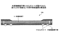
外部接続端子部17に相当する部分だけ外部接続端子部用レジスト25を除去して開口を形成してから、開口内で露出した配線14の上に保護金属層17aを形成する。保護金属層17aは例えば、ニッケル(Ni)めっきと金(Au)めっきの2層構造である。
センサ面側に用いる封止樹脂13Aよりも線膨張係数αの大きな樹脂を選定する。したがって、センサ面側に対してはセンサ面とマッチングの良い樹脂(αが小さい)を選定することで環境ストレスなどによる樹脂ハガレ等を防止し、実装面側に対しては実装基板に近い(αが大きい)樹脂の選定することで実装環境ストレス耐性を向上させることができる。
所定の機能を提供する機能面を有する半導体装置であって、
電極が形成された回路形成面と該回路形成面の反対側の背面とを有し、該回路形成面の一部が前記機能面として機能する半導体素子と、
該半導体素子の前記背面上に形成された配線と、
前記半導体素子の前記回路形成面と前記背面との間を貫通して延在し、前記電極と該配線とを電気的に接続する接続部と、
前記配線に接続され、前記半導体素子の前記背面側で前記半導体装置の外部に露出した外部接続端子と
を有することを特徴とする半導体装置。
付記1記載の半導体装置であって、
前記配線は封止樹脂により封止され、前記外部接続端子は該封止樹脂の表面から突出していることを特徴とする半導体装置。
付記2記載の半導体装置であって、
前記外部接続端子に、はんだボール、はんだコート、のうちいずれか一つが設けられていることを特徴とする半導体装置。
付記1記載の半導体装置であって、
前記配線は封止樹脂により封止され、前記外部接続端子は該封止樹脂に設けられた開口内で露出していることを特徴とする半導体装置。
付記4記載の半導体装置であって、
前記外部接続端子に、はんだボール、はんだコート、前記外部接続端子よりも小さい面積の突状端子、のうちいずれか一つが設けられていることを特徴とする半導体装置。
付記1記載の半導体装置であって、
前記半導体素子の前記回路形成面は、前記機能面が露出するように封止樹脂により封止され、該封止樹脂は前記半導体素子の側面の少なくとも一部を覆っていることを特徴とする半導体装置。
付記6記載の半導体装置であって、
前記半導体素子の側面は前記回路形成面に垂直な面から傾斜した傾斜面を含み、該傾斜面が前記封止樹脂により覆われていることを特徴とする半導体装置。
付記1記載の半導体装置であって、
前記半導体素子の前記背面に形成された前記配線は、前記外部接続用端子が露出するように封止樹脂により封止され、該封止樹脂は前記半導体素子の側面の少なくとも一部を覆っていることを特徴とする半導体装置。
付記8記載の半導体装置であって、
前記半導体素子の側面は前記背面に垂直な面から傾斜した傾斜面を含み、該傾斜面が前記封止樹脂により覆われていることを特徴とする半導体装置。
付記1記載の半導体装置であって、
前記半導体素子の前記回路形成面は、前記機能面が露出するように第1の封止樹脂により封止され、
前記半導体素子の前記背面に形成された前記配線は、前記外部接続端子が露出するように第2の封止樹脂により封止され、
前記第1の封止樹脂と前記第2の封止樹脂は、特性が異なる樹脂であることを特徴とする半導体装置。
付記1乃至10記載の半導体装置であって、
前記機能面に、前記半導体素子の回路形成面に形成された配線と同じ材料で形成された認識マークが設けられていることを特徴とする半導体装置。
付記1乃至11のうちいずれか一項記載の半導体装置であって、
前記半導体素子の前記機能面は、指紋検出用のセンサ面であることを特徴とする半導体装置。
電極が形成された回路形成面と該回路形成面の反対側の背面とを有し、該回路形成面の一部が所定の機能を提供する機能面として機能する半導体素子を有する、複数の半導体装置の製造方法であって
基板に整列して形成された複数の前記半導体素子の各々において、電極に電気的に接続され、前記半導体素子の前記回路形成面と前記背面との間を貫通して延在する接続部を導電部材により形成し、
前記半導体素子の各々において、該接続部に接続された配線を前記背面上に形成し、
前記半導体素子の各々において、該配線に接続された外部接続端子を形成し、
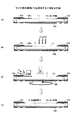
前記半導体素子を前記基板に形成された状態で、前記機能面及び前記外部接続端子が露出するように一括して樹脂封止し、
複数の前記半導体装置が基板中で形成された状態で、前記半導体装置の各々に電気的試験を施し、
前記基板を前記半導体素子の境界部分で切断して個片化することにより複数の前記半導体装置を一括して形成する
ことを特徴とする半導体装置の製造方法。
付記13記載の半導体装置の製造方法であって、
前記樹脂封止は金型を用いた樹脂の圧縮成型法により行ない、該金型は前記機能面に対応する位置に突出部を有しており、該金型と前記基板との間に該樹脂に対して密着しないシート在を介在させることを特徴とする半導体装置の製造方法。
付記13記載の半導体装置の製造方法であって、
前記樹脂封止の工程は、
前記基板に形成された複数の前記半導体素子の前記回路形成面上に、前記機能面以外の部分に相当する部分に開口を有する印刷マスクを配置し、
該印刷マスクを介して液状の樹脂を前記回路形成面に塗布し、
該液状の樹脂を硬化させてから前記前記印刷マスクを取り外す
ことを含むことを特徴とする半導体装置の製造方法。
付記13記載の半導体装置の製造方法であって、
前記樹脂封止の工程の後に、前記機能面及び外部接続端子の少なくとも一方に対してアッシング処理を行ない、前記樹脂封止による樹脂バリを除去することを特徴とする半導体装置の製造方法。
付記13記載の半導体装置の製造方法であって、
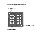
前記半導体素子の前記回路形成面に配線を形成する際に、前記機能面に該配線と同時に認識マークを形成し、
該認識マークを用いて前記境界部分を認識しながら、前記基板を切断して前記半導体装置を個片化することを特徴とする半導体装置の製造方法。
付記17記載の半導体装置の製造方法であって、
前記基板を切断して前記半導体装置を個片化する前に、前記認識マークを用いて前記境界部分を認識しながら、前記切断で削り取られる部分の幅より大きい幅の溝を前記境界部分に沿って形成することを特徴とする半導体装置の製造方法。
付記13記載の半導体装置の製造方法であって、
前記半導体素子の前記背面に前記外部接続端子を形成する際に、前記外部接続端子と同時に認識マークを形成し、
該認識マークを用いて前記境界部分を認識しながら、前記基板を切断して前記半導体装置を個片化することを特徴とする半導体装置の製造方法。
付記19記載の半導体装置の製造方法であって、
前記基板を切断して前記半導体装置を個片化する前に、前記認識マークを用いて前記境界部分を認識しながら、前記切断で削り取られる部分の幅より大きい幅の溝を前記境界部分に沿って形成することを特徴とする半導体装置の製造方法。
11 半導体素子
11a 電極
11b センサ面
11c,11d 傾斜面
12 外部接続端子
12a 保護金属層
13A,13B 封止樹脂
14 配線
15 接続部
16 絶縁層
17 外部接続端子部
17a 保護金属層
18 はんだボール
19 はんだコート
20 突状端子
23 配線レジスト
24 外部接続端子用レジスト
26,27 ダイシングブレード
30 上型
31A,31B 下型
32 弾性シート材
33 シート材
34,37 印刷マスク
35,38 マスク
36,39 パターニングマスク
40,41 認識マーク
Claims (1)
- 所定の機能を提供する機能面を有する半導体装置であって、
電極が形成された回路形成面と該回路形成面の反対側の背面とを有し、該回路形成面の一部が前記機能面として機能する半導体素子と、
前記回路形成面に設けられた電極と、
前記回路形成面の前記機能面以外を覆う絶縁層と、
該絶縁層上に形成され、前記回路形成面の前記電極に接続された第1の配線と、
前記絶縁層と前記第1の配線とを覆う第1の封止樹脂と、
前記半導体素子の前記背面上に形成された第2の配線と、
前記第2の配線を覆う第2の封止樹脂と、
前記半導体素子の前記回路形成面と前記背面との間を貫通して延在し、前記第1の配線と前記第2の配線とを電気的に接続する接続部と、
前記第2の配線に接続され、該第2の封止樹脂の表面から突出し、前記半導体素子の前記背面側で前記半導体装置の外部に露出した外部接続端子と
を有し、
前記半導体素子の側面は、前記第1の封止樹脂に覆われた前記回路形成面側の第1の傾斜面と、前記第2の封止樹脂に覆われた前記背面側の第2の傾斜面と、前記第1及び第2の傾斜面の間に位置し前記第1及び第2の封止樹脂のいずれにも覆われない露出面とを有することを特徴とする半導体装置。
Priority Applications (3)
| Application Number | Priority Date | Filing Date | Title |
|---|---|---|---|
| JP2005093001A JP4731191B2 (ja) | 2005-03-28 | 2005-03-28 | 半導体装置及び半導体装置の製造方法 |
| US11/209,791 US7586185B2 (en) | 2005-03-28 | 2005-08-24 | Semiconductor device having a functional surface |
| US12/458,995 US20090291515A1 (en) | 2005-03-28 | 2009-07-29 | Semiconductor device and a semiconductor device manufacturing method |
Applications Claiming Priority (1)
| Application Number | Priority Date | Filing Date | Title |
|---|---|---|---|
| JP2005093001A JP4731191B2 (ja) | 2005-03-28 | 2005-03-28 | 半導体装置及び半導体装置の製造方法 |
Related Child Applications (1)
| Application Number | Title | Priority Date | Filing Date |
|---|---|---|---|
| JP2011033300A Division JP2011097122A (ja) | 2011-02-18 | 2011-02-18 | 半導体装置の製造方法 |
Publications (2)
| Publication Number | Publication Date |
|---|---|
| JP2006278552A JP2006278552A (ja) | 2006-10-12 |
| JP4731191B2 true JP4731191B2 (ja) | 2011-07-20 |
Family
ID=37034381
Family Applications (1)
| Application Number | Title | Priority Date | Filing Date |
|---|---|---|---|
| JP2005093001A Expired - Fee Related JP4731191B2 (ja) | 2005-03-28 | 2005-03-28 | 半導体装置及び半導体装置の製造方法 |
Country Status (2)
| Country | Link |
|---|---|
| US (2) | US7586185B2 (ja) |
| JP (1) | JP4731191B2 (ja) |
Families Citing this family (30)
| Publication number | Priority date | Publication date | Assignee | Title |
|---|---|---|---|---|
| JP4837971B2 (ja) * | 2005-10-07 | 2011-12-14 | ルネサスエレクトロニクス株式会社 | 半導体装置の製造方法 |
| JP4904769B2 (ja) * | 2005-10-21 | 2012-03-28 | 富士通セミコンダクター株式会社 | 半導体装置 |
| JP5028988B2 (ja) * | 2006-12-13 | 2012-09-19 | ヤマハ株式会社 | 半導体装置の製造方法 |
| TWI325618B (en) * | 2007-01-02 | 2010-06-01 | Chipmos Technologies Inc | Film type package for fingerprint sensor |
| JP5217183B2 (ja) * | 2007-02-26 | 2013-06-19 | カシオ計算機株式会社 | 画像読取装置 |
| JP5122184B2 (ja) * | 2007-05-30 | 2013-01-16 | オンセミコンダクター・トレーディング・リミテッド | 半導体装置及びその製造方法 |
| TWI364793B (en) * | 2007-05-08 | 2012-05-21 | Mutual Pak Technology Co Ltd | Package structure for integrated circuit device and method of the same |
| WO2009031586A1 (ja) * | 2007-09-06 | 2009-03-12 | Murata Manufacturing Co., Ltd. | 回路基板及び回路基板の製造方法 |
| JP2009117699A (ja) * | 2007-11-08 | 2009-05-28 | Shinko Electric Ind Co Ltd | 半導体パッケージ用部品及び半導体パッケージ用部品の製造方法 |
| JP5115295B2 (ja) * | 2008-04-11 | 2013-01-09 | 株式会社デンソー | 半導体装置およびその製造方法 |
| JP5126370B2 (ja) * | 2008-12-16 | 2013-01-23 | 株式会社村田製作所 | 回路モジュール |
| US8264067B2 (en) * | 2009-10-09 | 2012-09-11 | Taiwan Semiconductor Manufacturing Company, Ltd. | Through silicon via (TSV) wire bond architecture |
| WO2011045836A1 (ja) * | 2009-10-14 | 2011-04-21 | 国立大学法人東北大学 | センサ装置およびセンサ装置の製造方法 |
| NO20093601A1 (no) * | 2009-12-29 | 2011-06-30 | Idex Asa | Overflatesensor |
| US8654537B2 (en) * | 2010-12-01 | 2014-02-18 | Apple Inc. | Printed circuit board with integral radio-frequency shields |
| US8279625B2 (en) | 2010-12-14 | 2012-10-02 | Apple Inc. | Printed circuit board radio-frequency shielding structures |
| FR2970117B1 (fr) * | 2010-12-29 | 2013-09-20 | St Microelectronics Crolles 2 | Procédé de fabrication d'une puce de circuit intégré a connexion par la face arrière |
| JP2012195388A (ja) * | 2011-03-15 | 2012-10-11 | Toshiba Corp | 半導体装置の製造方法及び半導体装置 |
| US9179538B2 (en) | 2011-06-09 | 2015-11-03 | Apple Inc. | Electromagnetic shielding structures for selectively shielding components on a substrate |
| US8836478B2 (en) | 2011-09-25 | 2014-09-16 | Authentec, Inc. | Electronic device including finger sensor and related methods |
| KR101356143B1 (ko) * | 2012-05-15 | 2014-01-27 | 크루셜텍 (주) | 지문센서 패키지 및 그 제조방법 |
| JP5966653B2 (ja) * | 2012-06-20 | 2016-08-10 | 富士通株式会社 | 半導体装置及び半導体装置の製造方法 |
| US9362236B2 (en) | 2013-03-07 | 2016-06-07 | Taiwan Semiconductor Manufacturing Company, Ltd. | Package structures and methods for forming the same |
| NL2012891B1 (en) * | 2013-06-05 | 2016-06-21 | Apple Inc | Biometric sensor chip having distributed sensor and control circuitry. |
| CN106269581B (zh) * | 2015-06-10 | 2019-10-18 | 鸿劲科技股份有限公司 | 指纹辨识电子元件作业装置及其应用的测试分类设备 |
| TWI537837B (zh) * | 2015-06-11 | 2016-06-11 | 南茂科技股份有限公司 | 指紋辨識晶片封裝結構及其製作方法 |
| CN110077657B (zh) * | 2018-01-26 | 2021-03-09 | 致伸科技股份有限公司 | 指纹辨识模块包装方法 |
| CN113380690B (zh) * | 2021-06-10 | 2023-06-16 | 西安微电子技术研究所 | 一种塑封器件湿法开帽的保护方法 |
| WO2023080089A1 (ja) * | 2021-11-05 | 2023-05-11 | ローム株式会社 | 半導体装置の製造方法 |
| WO2023095918A1 (ja) * | 2021-11-29 | 2023-06-01 | 凸版印刷株式会社 | インレット及びカード型媒体 |
Family Cites Families (27)
| Publication number | Priority date | Publication date | Assignee | Title |
|---|---|---|---|---|
| US4872825A (en) * | 1984-05-23 | 1989-10-10 | Ross Milton I | Method and apparatus for making encapsulated electronic circuit devices |
| US5319242A (en) * | 1992-03-18 | 1994-06-07 | Motorola, Inc. | Semiconductor package having an exposed die surface |
| US5682062A (en) * | 1995-06-05 | 1997-10-28 | Harris Corporation | System for interconnecting stacked integrated circuits |
| US6498074B2 (en) * | 1996-10-29 | 2002-12-24 | Tru-Si Technologies, Inc. | Thinning and dicing of semiconductor wafers using dry etch, and obtaining semiconductor chips with rounded bottom edges and corners |
| US6049124A (en) * | 1997-12-10 | 2000-04-11 | Intel Corporation | Semiconductor package |
| US6620731B1 (en) * | 1997-12-18 | 2003-09-16 | Micron Technology, Inc. | Method for fabricating semiconductor components and interconnects with contacts on opposing sides |
| JP3497722B2 (ja) * | 1998-02-27 | 2004-02-16 | 富士通株式会社 | 半導体装置及びその製造方法及びその搬送トレイ |
| KR100282426B1 (ko) * | 1999-03-17 | 2001-02-15 | 김영환 | 스마트 파워 소자 및 그의 제조 방법 |
| JP3772066B2 (ja) * | 2000-03-09 | 2006-05-10 | 沖電気工業株式会社 | 半導体装置 |
| JP3879816B2 (ja) * | 2000-06-02 | 2007-02-14 | セイコーエプソン株式会社 | 半導体装置及びその製造方法、積層型半導体装置、回路基板並びに電子機器 |
| JP3951091B2 (ja) * | 2000-08-04 | 2007-08-01 | セイコーエプソン株式会社 | 半導体装置の製造方法 |
| JP2002150256A (ja) | 2000-11-06 | 2002-05-24 | Dainippon Printing Co Ltd | 指紋センサ付きicモジュール |
| JPWO2002095834A1 (ja) * | 2001-05-18 | 2004-09-09 | 三洋電機株式会社 | 薄膜トランジスタ及びアクティブマトリクス型表示装置及びそれらの製造方法 |
| US6668449B2 (en) * | 2001-06-25 | 2003-12-30 | Micron Technology, Inc. | Method of making a semiconductor device having an opening in a solder mask |
| JP4561950B2 (ja) * | 2001-08-08 | 2010-10-13 | 信越化学工業株式会社 | 角形基板 |
| US6759745B2 (en) * | 2001-09-13 | 2004-07-06 | Texas Instruments Incorporated | Semiconductor device and manufacturing method thereof |
| JP3956199B2 (ja) * | 2002-02-20 | 2007-08-08 | シャープ株式会社 | 固体撮像装置の製造方法およびその製造方法において使用するマスク |
| JP3766034B2 (ja) * | 2002-02-20 | 2006-04-12 | 富士通株式会社 | 指紋センサ装置及びその製造方法 |
| JP2003282791A (ja) * | 2002-03-20 | 2003-10-03 | Fujitsu Ltd | 接触型センサ内蔵半導体装置及びその製造方法 |
| JP2004140037A (ja) * | 2002-10-15 | 2004-05-13 | Oki Electric Ind Co Ltd | 半導体装置、及びその製造方法 |
| TW586677U (en) * | 2003-01-22 | 2004-05-01 | Via Tech Inc | Stack structure of chip package |
| JP2004319678A (ja) | 2003-04-15 | 2004-11-11 | Fujitsu Ltd | 指紋センサ装置及びその製造方法 |
| TWI226094B (en) * | 2003-07-21 | 2005-01-01 | Advanced Semiconductor Eng | Process for testing IC wafer |
| KR100537892B1 (ko) * | 2003-08-26 | 2005-12-21 | 삼성전자주식회사 | 칩 스택 패키지와 그 제조 방법 |
| US7091124B2 (en) * | 2003-11-13 | 2006-08-15 | Micron Technology, Inc. | Methods for forming vias in microelectronic devices, and methods for packaging microelectronic devices |
| US7230318B2 (en) * | 2003-12-24 | 2007-06-12 | Agency For Science, Technology And Research | RF and MMIC stackable micro-modules |
| WO2006043122A1 (en) * | 2004-10-21 | 2006-04-27 | Infineon Technologies Ag | Semiconductor package and method to produce the same |
-
2005
- 2005-03-28 JP JP2005093001A patent/JP4731191B2/ja not_active Expired - Fee Related
- 2005-08-24 US US11/209,791 patent/US7586185B2/en not_active Expired - Fee Related
-
2009
- 2009-07-29 US US12/458,995 patent/US20090291515A1/en not_active Abandoned
Also Published As
| Publication number | Publication date |
|---|---|
| JP2006278552A (ja) | 2006-10-12 |
| US7586185B2 (en) | 2009-09-08 |
| US20060214294A1 (en) | 2006-09-28 |
| US20090291515A1 (en) | 2009-11-26 |
Similar Documents
| Publication | Publication Date | Title |
|---|---|---|
| JP4731191B2 (ja) | 半導体装置及び半導体装置の製造方法 | |
| US7163843B2 (en) | Semiconductor component of semiconductor chip size with flip-chip-like external contacts, and method of producing the same | |
| US6706547B2 (en) | Method of manufacturing a circuit device with trenches in a conductive foil | |
| US6884652B2 (en) | Semiconductor package free of substrate and fabrication method thereof | |
| KR100319609B1 (ko) | 와이어 어래이드 칩 사이즈 패키지 및 그 제조방법 | |
| US7939383B2 (en) | Method for fabricating semiconductor package free of substrate | |
| CN101383301B (zh) | 形成倒装芯片突起载体式封装的方法 | |
| US6841884B2 (en) | Semiconductor device | |
| CN112071822A (zh) | 半导体装置及制造半导体装置的方法 | |
| US7053492B2 (en) | Circuit device and method of manufacturing the same | |
| KR20020075188A (ko) | 회로 장치의 제조 방법 | |
| US7423340B2 (en) | Semiconductor package free of substrate and fabrication method thereof | |
| CN105938802A (zh) | 树脂密封型半导体装置及其制造方法 | |
| US20070249101A1 (en) | Method for fabricating semiconductor package free of substrate | |
| KR100829613B1 (ko) | 반도체 칩 패키지 및 그 제조 방법 | |
| CN101256994A (zh) | 半导体器件及其制造方法 | |
| JP2011097122A (ja) | 半導体装置の製造方法 | |
| JP3722784B2 (ja) | 半導体装置 | |
| JP4631223B2 (ja) | 半導体実装体およびそれを用いた半導体装置 | |
| JP4155994B2 (ja) | 半導体装置およびその製造方法 | |
| TW479305B (en) | A semiconductor package and a wafer level packaging method | |
| US20050184368A1 (en) | Semiconductor package free of substrate and fabrication method thereof | |
| JP2001223228A (ja) | 半導体パッケージ用基板とその製造方法とその装置 | |
| JP5036217B2 (ja) | 半導体装置及びその製造方法 | |
| JP2003158217A (ja) | 半導体装置およびその製造方法 |
Legal Events
| Date | Code | Title | Description |
|---|---|---|---|
| A621 | Written request for application examination |
Free format text: JAPANESE INTERMEDIATE CODE: A621 Effective date: 20080125 |
|
| A711 | Notification of change in applicant |
Free format text: JAPANESE INTERMEDIATE CODE: A712 Effective date: 20080728 |
|
| A977 | Report on retrieval |
Free format text: JAPANESE INTERMEDIATE CODE: A971007 Effective date: 20100308 |
|
| A131 | Notification of reasons for refusal |
Free format text: JAPANESE INTERMEDIATE CODE: A131 Effective date: 20100406 |
|
| A521 | Request for written amendment filed |
Free format text: JAPANESE INTERMEDIATE CODE: A523 Effective date: 20100607 |
|
| A131 | Notification of reasons for refusal |
Free format text: JAPANESE INTERMEDIATE CODE: A131 Effective date: 20100629 |
|
| A521 | Request for written amendment filed |
Free format text: JAPANESE INTERMEDIATE CODE: A523 Effective date: 20100827 |
|
| A02 | Decision of refusal |
Free format text: JAPANESE INTERMEDIATE CODE: A02 Effective date: 20101124 |
|
| A521 | Request for written amendment filed |
Free format text: JAPANESE INTERMEDIATE CODE: A523 Effective date: 20110218 |
|
| A911 | Transfer to examiner for re-examination before appeal (zenchi) |
Free format text: JAPANESE INTERMEDIATE CODE: A911 Effective date: 20110225 |
|
| A01 | Written decision to grant a patent or to grant a registration (utility model) |
Free format text: JAPANESE INTERMEDIATE CODE: A01 Effective date: 20110322 |
|
| A61 | First payment of annual fees (during grant procedure) |
Free format text: JAPANESE INTERMEDIATE CODE: A61 Effective date: 20110419 |
|
| FPAY | Renewal fee payment (event date is renewal date of database) |
Free format text: PAYMENT UNTIL: 20140428 Year of fee payment: 3 |
|
| R150 | Certificate of patent or registration of utility model |
Free format text: JAPANESE INTERMEDIATE CODE: R150 |
|
| LAPS | Cancellation because of no payment of annual fees |