JP4797366B2 - Pyroelectric infrared detector - Google Patents
Pyroelectric infrared detector Download PDFInfo
- Publication number
- JP4797366B2 JP4797366B2 JP2004341072A JP2004341072A JP4797366B2 JP 4797366 B2 JP4797366 B2 JP 4797366B2 JP 2004341072 A JP2004341072 A JP 2004341072A JP 2004341072 A JP2004341072 A JP 2004341072A JP 4797366 B2 JP4797366 B2 JP 4797366B2
- Authority
- JP
- Japan
- Prior art keywords
- terminal
- circuit
- operational amplifier
- turned
- feedback circuit
- Prior art date
- Legal status (The legal status is an assumption and is not a legal conclusion. Google has not performed a legal analysis and makes no representation as to the accuracy of the status listed.)
- Expired - Fee Related
Links
Images





Landscapes
- Radiation Pyrometers (AREA)
- Photometry And Measurement Of Optical Pulse Characteristics (AREA)
Description
本発明は、焦電素子を用いて、人体から輻射される赤外線エネルギーを検出し、人体の存在や移動の検知を行なったり、輻射エネルギーや室温を検出することで放射温度計として機能する赤外線検出装置に関するものである。 The present invention uses a pyroelectric element to detect infrared energy radiated from the human body, detect the presence or movement of the human body, and detect infrared energy and room temperature to detect infrared energy and function as a radiation thermometer. It relates to the device.
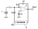
図10は、従来の焦電型赤外線検出装置の基本構成を示し、焦電素子1は一端をグランドに接続し、他端を演算増幅器2の反転入力端子に接続しており、演算増幅器2の出力端子−反転入力端子間には、コンデンサからなる帰還容量Cfを接続して交流帰還回路を構成している。また、演算増幅器2の出力端子−反転入力端子間には、さらに直流帰還回路3と入力抵抗Riとの直列回路を設けて、入力抵抗Riによって帰還を行っている。また、演算増幅器2の非反転入力端子にはバイアス電位Vrを印加している。このような回路は、熱線感知時に焦電素子1で発生する電流信号を電圧信号に変換して出力する電流電圧変換回路を構成するものである。なお、演算増幅器2の反転入力端子をSin、演算増幅器2の出力端子をSout、直流帰還回路3の出力端子をSfoとする。
FIG. 10 shows a basic configuration of a conventional pyroelectric infrared detection device. The
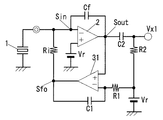
このような焦電型赤外線検出装置は、人体から輻射される赤外線エネルギーを検出し、人体の存在や移動の検知を行なったり、輻射エネルギーや室温を検出することで放射温度計として機能するものである。一般に人体検知を行う場合の検出周波数は1Hz中心であるので、本電流電圧変換回路の後段に設けられる電圧増幅部(図示無し)において、1Hzを中心とした0.1〜10Hz付近の周波数帯が選択的に増幅される。そこで図11に示すように、演算増幅器2の出力端子SoutはコンデンサC2と抵抗R2とから構成されるハイパスフィルタに接続される場合が多く、0.1Hz以上の周波数成分を通過させている。ここで、コンデンサC2の一端は演算増幅器2の出力端子Soutに接続され、コンデンサC2の他端は抵抗R2の一端に接続され、抵抗R2の他端はバイアス電位Vrに接続されており、コンデンサC2と抵抗R2との接続点Vx1が本焦電型赤外線検出装置の出力となる。
Such a pyroelectric infrared detector functions as a radiation thermometer by detecting infrared energy radiated from the human body, detecting the presence and movement of the human body, and detecting radiant energy and room temperature. is there. In general, the detection frequency when human body detection is performed is centered at 1 Hz. Therefore, in a voltage amplification unit (not shown) provided at the subsequent stage of the current-voltage conversion circuit, a frequency band around 0.1 Hz centering on 1 Hz is present. Is selectively amplified. Therefore, as shown in FIG. 11, the output terminal Sout of the
また図11は、図10の直流帰還回路3の具体回路も示しており、直流帰還回路3は、非反転入力端子に演算増幅器2の出力を接続した演算増幅器31と、演算増幅器31の出力端子−反転入力端子間に接続したコンデンサC1と、演算増幅器31の反転入力端子−バイアス電位Vr間に接続した抵抗R1とからなる積分回路で構成され、演算増幅器31の出力が直流帰還回路3の出力となる。
FIG. 11 also shows a specific circuit of the
このような構成の電流電圧変換回路においては、焦電素子1から出力される電流信号は帰還容量Cfのインピーダンスを用いて電圧信号に変換され、変換インピーダンスの周波数特性がバンドパスフィルタの役割を果たす。このバンドパスフィルタの中心周波数ω0、選択度Qは、数1で表される。
In the current-voltage conversion circuit having such a configuration, the current signal output from the
そして、焦電素子1の最大のアプリケーションである人体検知における検出周波数が1Hz中心であることから、0.1Hz以上の周波数帯では帰還容量Cfのインピーダンス特性によって電圧信号の出力特性が決まるようにしようとすると、中心周波数ω0は0.1Hz以下でなければならない。したがって、この電流電圧変換回路の時定数は非常に遅くなる。
Since the detection frequency in human body detection, which is the largest application of the
また、ノイズ成分の1つとして入力抵抗Riによる熱雑音が支配的であるので、この熱雑音を抑制するために、通常は入力抵抗Riの値を1T(テラ)Ω以上の高抵抗としている。このような高抵抗は一般に温度変化によって抵抗値が大きく変動する特性を有している。(例えば、特許文献1参照)
上記従来例のように、遅い時定数を有する電流電圧変換回路においては、電源投入から回路動作が安定するまでの間(回路安定時間)や、回路動作中に大きな外来ノイズが印加された場合等に動作点が飽和してしまうと、元の正常な状態に復帰するのに長い時間を必要とするという問題があった。 In the current-voltage conversion circuit having a slow time constant as in the above-mentioned conventional example, the time from when the power is turned on until the circuit operation is stabilized (circuit stabilization time), or when a large external noise is applied during the circuit operation, etc. When the operating point is saturated, there is a problem that it takes a long time to return to the original normal state.
ここで、図11に示すように直流帰還回路3を積分回路で構成した電流電圧変換回路についてのシミュレーション結果を、図12〜図14に示す。ここで回路定数は、帰還容量Cf=10pF、入力抵抗Ri=3TΩ、コンデンサC1=10nF、抵抗R1=6GΩとしている。
Here, simulation results for the current-voltage conversion circuit in which the
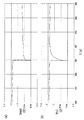
図12は電源投入時、および外来ノイズ印加時の過渡解析の結果であり、図12(a)は演算増幅器2の出力端子Soutの電圧波形、図12(b)はコンデンサC2と抵抗R2との接続点Vx1の電圧波形(ハイパスフィルタの出力波形)を各々示す。そして時間t=0で、演算増幅器2,31の電源電位3V、バイアス電位Vr=1.5Vを印加し、演算増幅器2の反転入力端子Sinには1Hzの正弦波からなる電流信号を時間t=0より入力し続ける。さらに、時間t=500秒(電源投入後の安定動作している状態)には、外来ノイズを想定して演算増幅器2の反転入力端子Sinに60pCの負の電荷を印加する。ここで、図12(a)に示すように演算増幅器2の出力端子Soutの電圧波形は非常に遅い周波数で変動しているが、図12(b)に示すように接続点Vx1の電圧波形では抵抗R2、コンデンサC2によるハイパスフィルタによってその変動はカットされており、後段の回路に非常に遅い周波数の変動が伝わらないようになっている。
FIG. 12 shows the results of transient analysis when the power is turned on and when external noise is applied. FIG. 12A shows the voltage waveform at the output terminal Sout of the
そして、電源投入時は演算増幅器2の出力端子Soutの電位が正側に飽和しており、図13(a)(b)に時間t=23〜30秒における各波形の拡大図を示すように、電源投入後約25秒間(時間t=0〜25秒)は入力信号に対して正常に応答せず、回路動作が安定していない。
Then, when the power is turned on, the potential of the output terminal Sout of the
また、時間t=500秒で外来ノイズが印加された場合には、演算増幅器2の出力端子Soutの電位が負側に飽和しており、図14(a)(b)に時間t=594〜610秒における各波形の拡大図を示すように、外来ノイズ印加後約100秒間(時間t=500〜600秒)は入力信号に対して正常に応答せず、正常動作に復帰していない。
Further, when external noise is applied at time t = 500 seconds, the potential of the output terminal Sout of the
本発明は、上記事由に鑑みてなされたものであり、その目的は、電源投入から回路動作が安定するまでの時間が短く、且つ回路動作時に外来ノイズが印加されても速やかに復帰可能な焦電型赤外線検出装置を提供することにある。 The present invention has been made in view of the above reasons, and its purpose is to shorten the time from when the power is turned on until the circuit operation is stabilized, and to enable quick recovery even when external noise is applied during circuit operation. An object is to provide an electric infrared detector.
請求項1の発明は、熱線感知時に電流信号を発生する焦電素子と、第1のコンデンサからなる交流帰還回路、および直流帰還回路と第1の抵抗素子との直列回路を入出力間に接続した演算増幅器で構成されて前記電流信号を電圧信号に変換して出力する電流電圧変換回路とを備え、交流帰還回路を演算増幅器の出力端子−反転入力端子間に接続し、直流帰還回路の一端を演算増幅器の出力側に接続し、第1の抵抗素子を直流帰還回路の他端−演算増幅器の反転入力端子間に接続し、焦電素子を演算増幅器の反転入力端子に接続して、リミッタ回路は、ソース端子を第1の抵抗素子の一端に接続し、ゲート端子、ドレイン端子を第1の抵抗素子の他端に接続した第1のMOSトランジスタと、ゲート端子、ドレイン端子を第1の抵抗素子の一端に接続し、ソース端子を第1の抵抗素子の他端に接続した第2のMOSトランジスタとから構成され、第1、第2のMOSトランジスタがP型の場合は各基板端子を電源電位に接続し、第1、第2のMOSトランジスタがN型の場合は各基板端子をグランドに接続し、電源電位とグランドとの間に接続された第2の抵抗素子と第2のコンデンサとの直列回路と、第1,第2のMOSトランジスタのうち少なくともいずれか一方のMOSトランジスタのゲート端子とドレイン端子との間に接続された第1のスイッチ素子と、第2の抵抗素子および第2のコンデンサの接続中点と前記少なくともいずれか一方のMOSトランジスタのゲート端子との間に接続された第2のスイッチ素子を有して、電源投入後、第1のスイッチ素子がオフ、第2のスイッチ素子がオンして、前記少なくともいずれか一方のMOSトランジスタがオンし、第2のコンデンサの充電電圧によって前記少なくともいずれか一方のMOSトランジスタがオフした後、第1のスイッチ素子がオン、第2のスイッチ素子がオフすることによって、前記少なくともいずれか一方のMOSトランジスタを、電源投入時に所定期間導通させることを特徴とする。 According to the first aspect of the present invention, a pyroelectric element that generates a current signal when detecting heat rays, an AC feedback circuit including a first capacitor, and a series circuit of the DC feedback circuit and the first resistance element are connected between the input and output. And a current-voltage conversion circuit configured to convert the current signal into a voltage signal and output the voltage signal. An AC feedback circuit is connected between the output terminal and the inverting input terminal of the operational amplifier, and one end of the DC feedback circuit. Is connected to the output side of the operational amplifier, the first resistance element is connected between the other end of the DC feedback circuit and the inverting input terminal of the operational amplifier, the pyroelectric element is connected to the inverting input terminal of the operational amplifier, and the limiter The circuit includes a first MOS transistor having a source terminal connected to one end of the first resistance element, a gate terminal and a drain terminal connected to the other end of the first resistance element, and a gate terminal and a drain terminal connected to the first resistance element. One end of resistance element And a second MOS transistor having a source terminal connected to the other end of the first resistance element. When the first and second MOS transistors are P-type, each substrate terminal is connected to a power supply potential. When the first and second MOS transistors are N-type, each substrate terminal is connected to the ground, and a series circuit of a second resistor and a second capacitor connected between the power supply potential and the ground, Connection between the first switch element connected between the gate terminal and the drain terminal of at least one of the first and second MOS transistors, the second resistance element, and the second capacitor A second switch element connected between the midpoint and the gate terminal of at least one of the MOS transistors, and after power-on, the first switch element is turned off; The switch element is turned on, the at least one MOS transistor is turned on, and the first switch element is turned on after the at least one MOS transistor is turned off by the charging voltage of the second capacitor. When the two switch elements are turned off, at least one of the MOS transistors is made conductive for a predetermined period when the power is turned on.
この発明によれば、遅い時定数を有する電流電圧変換回路においても、電源投入から回路動作が安定するまでの時間が短く、且つ回路動作時に外来ノイズが印加されても速やかに復帰可能とすることができる。また、MOSトランジスタの基板端子から演算増幅器の反転入力端子へのリーク電流を小さくできるので、このリーク電流によるショットノイズ成分は無視できる程度に抑制可能で、S/N比の悪化を防ぐことができる。またリミッタ回路をMOSトランジスタで構成しているので、回路の集積化、小型化に有利となる。さらにリミッタ回路にスタートアップ回路を併用させることにより回路のさらなる小型化を図ることができる。 According to the present invention, even in a current-voltage conversion circuit having a slow time constant, the time from when the power is turned on until the circuit operation is stabilized is short, and even if external noise is applied during circuit operation, it can be quickly restored. Can do. Further, since the leakage current from the substrate terminal of the MOS transistor to the inverting input terminal of the operational amplifier can be reduced, the shot noise component due to this leakage current can be suppressed to a negligible level, and the deterioration of the S / N ratio can be prevented. . Further, since the limiter circuit is composed of MOS transistors, it is advantageous for circuit integration and miniaturization. Further, the circuit can be further reduced in size by using the start-up circuit together with the limiter circuit.
請求項2の発明は、請求項1において、前記リミッタ回路の各MOSトランジスタに第3の抵抗素子を各々直列接続したことを特徴とする。 According to a second aspect of the present invention, in the first aspect, a third resistance element is connected in series to each MOS transistor of the limiter circuit.
この発明によれば、第3の抵抗素子によって、PMOSトランジスタがオンしたときに、演算増幅器の反転入力端子−直流帰還回路の出力間の抵抗値が急激に低下することを抑制して、演算増幅器の出力の不連続性を抑えることができる。したがって、演算増幅器の出力の不連続性による誤動作を防止できる。 According to the present invention, when the PMOS transistor is turned on by the third resistance element, the resistance value between the inverting input terminal of the operational amplifier and the output of the DC feedback circuit is suppressed from abruptly decreasing. The output discontinuity can be suppressed. Therefore, malfunction due to the discontinuity of the output of the operational amplifier can be prevented.
以上説明したように、本発明では、リミッタ回路によって第1の抵抗素子両端の電位差を制限するので、電源投入から回路動作が安定するまでの時間が短く、且つ回路動作時に外来ノイズが印加されても速やかに復帰可能となるという効果がある。また、MOSトランジスタの基板端子から演算増幅器の反転入力端子へのリーク電流を小さくできるので、このリーク電流によるショットノイズ成分は無視できる程度に抑制可能で、S/N比の悪化を防ぐことができる。またリミッタ回路をMOSトランジスタで構成しているので、回路の集積化、小型化に有利となる。さらにリミッタ回路にスタートアップ回路を併用させることにより回路のさらなる小型化を図ることができる。 As described above, in the present invention, since the potential difference between both ends of the first resistance element is limited by the limiter circuit, the time from when the power is turned on until the circuit operation is stabilized is short, and external noise is applied during the circuit operation. Also has the effect of being able to return quickly. Further, since the leakage current from the substrate terminal of the MOS transistor to the inverting input terminal of the operational amplifier can be reduced, the shot noise component due to this leakage current can be suppressed to a negligible level, and the deterioration of the S / N ratio can be prevented. . Further, since the limiter circuit is composed of MOS transistors, it is advantageous for circuit integration and miniaturization. Further, the circuit can be further reduced in size by using the start-up circuit together with the limiter circuit.
以下、本発明の実施の形態を図面に基づいて説明する。 Hereinafter, embodiments of the present invention will be described with reference to the drawings.
(実施形態1)
本発明の焦電型赤外線検出装置の基本構成は図1に示されるように、図10に示す従来例における入力抵抗Riにリミッタ回路4を並列接続したものであり、他の構成は図10と同様であり、同様の構成には同一の符号を付して説明は省略する。
(Embodiment 1)
As shown in FIG. 1, the basic configuration of the pyroelectric infrared detecting device of the present invention is that the
リミッタ回路4は、入力抵抗Riに並列接続して入力抵抗Riの両端の電位差を制限している。
The
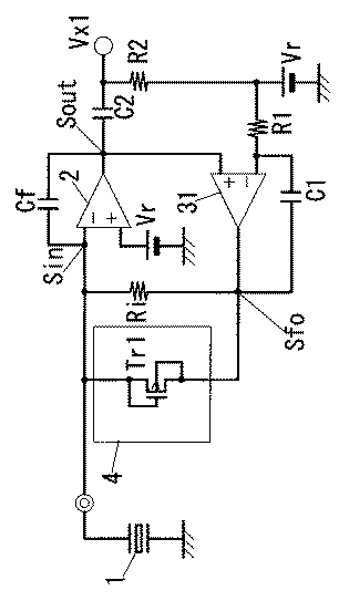
図2は、図1の直流帰還回路3、リミッタ回路4の具体回路を示しており、直流帰還回路3は、図11に示す従来例と同様の積分回路である。
FIG. 2 shows specific circuits of the
リミッタ回路4は、PMOSトランジスタTr1,Tr2が互いに逆並列接続して、入力抵抗Riに並列接続している。入力抵抗Riは一端を直流帰還回路3の出力端子Sfoに接続し、他端を演算増幅器2の反転入力端子Sinに接続しており、PMOSトランジスタTr1は、ソース端子を直流帰還回路3の出力端子Sfoに接続し、ゲート端子、ドレイン端子を反転入力端子Sinに接続し、PMOSトランジスタTr2は、ゲート端子、ドレイン端子を直流帰還回路3の出力端子Sfoに接続し、ソース端子を反転入力端子Sinに接続している。また、PMOSトランジスタTr1,Tr2の各基板端子は電源電位Vccに接続されている。このように、リミッタ回路4をPMOSトランジスタTr1,Tr2で構成することにより、集積化に有利となる。
In the
次に、図2に示す電流電圧変換回路についてのシミュレーション結果を、図3〜図5に示す。ここで回路定数は、帰還容量Cf=10pF、入力抵抗Ri=3TΩ、コンデンサC1=10nF、抵抗R1=6GΩとしている。 Next, simulation results for the current-voltage conversion circuit shown in FIG. 2 are shown in FIGS. Here, the circuit constants are a feedback capacity Cf = 10 pF, an input resistance Ri = 3 TΩ, a capacitor C1 = 10 nF, and a resistance R1 = 6 GΩ.
図3は電源投入時、および外来ノイズ印加時の過渡解析の結果であり、図3(a)は演算増幅器2の出力端子Soutの電圧波形、図3(b)はコンデンサC2と抵抗R2との接続点Vx1の電圧波形(ハイパスフィルタの出力波形)を各々示す。そして時間t=0で、演算増幅器2,31の電源電位3V(=Vcc)、バイアス電位Vr=1.5Vを印加し、演算増幅器2の反転入力端子Sinには1Hzの正弦波からなる電流信号を時間t=0より入力し続ける。さらに、時間t=500秒(電源投入後の安定動作している状態)には、外来ノイズを想定して演算増幅器2の反転入力端子Sinに60pCの負の電荷を印加する。
FIG. 3 shows the results of transient analysis when the power is turned on and when external noise is applied. FIG. 3 (a) shows the voltage waveform at the output terminal Sout of the
そして、電源投入時は演算増幅器2の出力端子Soutの電位が正側に変動しており、図4(a)(b)に時間t=0〜16秒における各波形の拡大図を示すように、電源投入直後、演算増幅器2の出力端子Soutおよび直流帰還回路3の出力端子Sfoの各電位が3Vまで上昇しようとすると、出力端子Sfoに接続したPMOSトランジスタTr1のソース電位も同様に上昇する。そして、端子Sout、Sfoの電位が2V付近まで上昇すると、PMOSトランジスタTr1のゲート−ソース間電圧Vgsがしきい値(負電圧)を超えて、PMOSトランジスタTr1がオンする。入力抵抗Riの両端がPMOSトランジスタTr1によって短絡されると、端子Sout、Sfoの各電位はそれ以上上昇しなくなり、飽和することなく低下する。したがって、時間t=0で電源投入して1〜2秒後には入力信号に対して正常に応答している。この動作は電源投入時のみでなく、演算増幅器2の出力端子Soutの電位が正側に変動するような外来ノイズが印加された場合(例えば、演算増幅器2の反転入力端子Sinに正の電荷が与えられた場合等)も同様である。
When the power is turned on, the potential of the output terminal Sout of the
さらに、時間t=500秒で、演算増幅器2の反転入力端子Sinに負の電荷を与える外来ノイズが印加された場合には、演算増幅器2の出力端子Soutの電位が負側に変動する。そして、図5(a)(b)に時間t=498〜505秒における各波形の拡大図を示すように、演算増幅器2の出力端子Soutおよび直流帰還回路3の出力端子Sfoの各電位が0Vまで下がろうとすると、出力端子Sfoに接続したPMOSトランジスタTr2のゲート電位も同様に下がる。そして、端子Sout、Sfoの電位が1V付近まで下がると、PMOSトランジスタTr2のゲート−ソース間電圧Vgsがしきい値(負電圧)を超えて、PMOSトランジスタTr2がオンする。入力抵抗Riの両端がPMOSトランジスタTr2によって短絡されると、端子Sout、Sfoの各電位はそれ以上下がらなくなり、飽和することなく上昇する。したがって、外来ノイズ印加後約1〜2秒後(時間t=501〜502秒)には入力信号に対して正常な応答を行う動作に復帰している。
Furthermore, when external noise that applies a negative charge to the inverting input terminal Sin of the
ここで、演算増幅器2の反転入力端子Sinに電流性のノイズ成分が存在すると出力に大きく影響し、特に、PN接合の逆バイアス時に発生するリーク電流は、電流性のショットノイズ成分を有するため注意が必要である。本実施形態では、演算増幅器2の反転入力端子Sinに影響するリーク電流として、PMOSトランジスタTr1の電源電位Vccに接続した基板(N型)端子からドレイン(P型)端子を介した反転入力端子Sinへのリーク電流、およびPMOSトランジスタTr2の電源電位Vccに接続した基板(N型)端子からソース(P型)端子を介した反転入力端子Sinへのリーク電流が存在するが、このPN接合の面積は、PMOSトランジスタTr1、Tr2のソース面積が影響するので、非常に小さな面積となり、このPN接合で生じるリーク電流のショットノイズ成分は無視できる程度に抑制でき、リーク電流によるS/N比の悪化を防ぐことができる。
Here, the presence of a current noise component at the inverting input terminal Sin of the
また、演算増幅器2の反転入力端子Sinの入力リーク電流も上記同様の理由によって小さくしなければならず、本実施形態では、内部回路をMOSトランジスタで構成した演算増幅器2を用いることで、入力リーク電流を抑制している。
Also, the input leakage current at the inverting input terminal Sin of the
なお、本実施形態ではP型のMOSトランジスタTr1,Tr2を用いて、各基板端子を電源電位Vccに接続しているが、N型のMOSトランジスタを用いる場合には、各基板端子をグランドに接続すれば同様に用いることができる。 In this embodiment, the P-type MOS transistors Tr1 and Tr2 are used to connect each substrate terminal to the power supply potential Vcc. However, when an N-type MOS transistor is used, each substrate terminal is connected to the ground. Then, it can be used similarly.
(参考例1)
図6は本参考例の焦電型赤外線検出装置の構成を示しており、実施形態1の図2とはリミッタ回路4の構成のみが異なるもので、同様の構成には同一の符号を付して説明は省略する。
( Reference Example 1 )
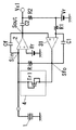
FIG. 6 shows the configuration of the pyroelectric infrared detection apparatus of the present reference example , which is different from FIG. 2 of the first embodiment only in the configuration of the
本参考例のリミッタ回路4は、PMOSトランジスタTr1,Tr2が互いに逆並列接続して、入力抵抗Riに並列接続している。入力抵抗Riは一端を直流帰還回路3の出力端子Sfoに接続し、他端を演算増幅器2の反転入力端子Sinに接続しており、PMOSトランジスタTr1は、ドレイン端子を直流帰還回路3の出力端子Sfoに接続し、ゲート端子、ソース端子、基板端子を反転入力端子Sinに接続し、PMOSトランジスタTr2は、ゲート端子、ソース端子、基板端子を直流帰還回路3の出力端子Sfoに接続し、ドレイン端子を反転入力端子Sinに接続している。このように、リミッタ回路4をPMOSトランジスタTr1,Tr2で構成することにより、集積化に有利となる。
In the
そして電源投入時、または正の外来ノイズ印加時に、演算増幅器2の出力端子Soutおよび直流帰還回路3の出力端子Sfoの各電位が3Vまで上昇しようとすると、出力端子Sfoに接続したPMOSトランジスタTr1のドレイン電位も同様に上昇する。そして、PMOSトランジスタTr1のドレイン(P型)端子から基板(N型)端子に向かって順方向のダイオード接合が形成されており、端子Sfoの電位>端子Sinの電位となる方向に一定以上の電位差が生じると、PMOSトランジスタTr1のドレイン(P型)端子−基板(N型)端子間がダイオードとして導通する。入力抵抗Riの両端がPMOSトランジスタTr1によって短絡されると、端子Sout、Sfoの各電位はそれ以上上昇しなくなり、飽和することなく低下する。したがって、電源投入あるいは外来ノイズを印加してから1〜2秒後には入力信号に対して正常に応答している。
When the potentials of the output terminal Sout of the
また、負の外来ノイズが印加されて、演算増幅器2の出力端子Soutおよび直流帰還回路3の出力端子Sfoの各電位が0Vまで下がろうとすると、出力端子Sfoに接続したPMOSトランジスタTr2の基板電位も同様に下がる。そして、PMOSトランジスタTr2のドレイン(P型)端子から基板(N型)端子に向かって順方向のダイオード接合が形成されており、端子Sinの電位>端子Sfoの電位となる方向に一定以上の電位差が生じると、PMOSトランジスタTr2のドレイン(P型)端子−基板(N型)端子間がダイオードとして導通する。入力抵抗Riの両端がPMOSトランジスタTr2によって短絡されると、端子Sout、Sfoの各電位はそれ以上下がらなくなり、飽和することなく上昇する。したがって、外来ノイズ印加後約1〜2秒後には入力信号に対して正常な応答を行う動作に復帰している。
Further, when negative external noise is applied and the respective potentials at the output terminal Sout of the
このような本参考例では、PMOSトランジスタTr1、Tr2の各PN接合部の特性を用いてリミッタ回路4を構成しているので、PMOSトランジスタTr1、Tr2の各トランジスタ特性を用いた場合に比べて、製造バラツキを小さくできる。
In this reference example , since the
(参考例2)
図7は本参考例の焦電型赤外線検出装置の構成を示しており、実施形態1の図2とはリミッタ回路4の構成のみが異なるもので、同様の構成には同一の符号を付して説明は省略する。
( Reference Example 2 )
FIG. 7 shows the configuration of the pyroelectric infrared detection apparatus of this reference example , which is different from FIG. 2 of the first embodiment only in the configuration of the
本参考例のリミッタ回路4は、PMOSトランジスタTr1が入力抵抗Riに並列接続している。入力抵抗Riは一端を直流帰還回路3の出力端子Sfoに接続し、他端を演算増幅器2の反転入力端子Sinに接続しており、PMOSトランジスタTr1は、ソース端子、基板端子を直流帰還回路3の出力端子Sfoに接続し、ドレイン端子、ゲート端子を反転入力端子Sinに接続している。このように、リミッタ回路4をPMOSトランジスタTr1で構成することにより、集積化に有利となる。
In the
そして電源投入時、または正の外来ノイズ印加時に、演算増幅器2の出力端子Soutおよび直流帰還回路3の出力端子Sfoの各電位が3Vまで上昇しようとすると、出力端子Sfoに接続したPMOSトランジスタTr1のソース電位も同様に上昇する。そして、端子Sout、Sfoの電位が2V付近まで上昇すると、PMOSトランジスタTr1のゲート−ソース間電圧Vgsがしきい値(負電圧)を超えて、PMOSトランジスタTr1がオンする。入力抵抗Riの両端がPMOSトランジスタTr1によって短絡されると、端子Sout、Sfoの各電位はそれ以上上昇しなくなり、飽和することなく低下する。したがって、電源投入あるいは外来ノイズを印加してから1〜2秒後には入力信号に対して正常に応答している。
When the potentials of the output terminal Sout of the
また、負の外来ノイズが印加されて、演算増幅器2の出力端子Soutおよび直流帰還回路3の出力端子Sfoの各電位が0Vまで下がろうとすると、出力端子Sfoに接続したPMOSトランジスタTr1の基板電位も同様に下がる。そして、PMOSトランジスタTr1のドレイン(P型)端子から基板(N型)端子に向かって順方向のダイオード接合が形成されており、端子Sinの電位>端子Sfoの電位となる方向に一定以上の電位差が生じると、PMOSトランジスタTr1のドレイン(P型)端子−基板(N型)端子間がダイオードとして導通する。入力抵抗Riの両端がPMOSトランジスタTr1によって短絡されると、端子Sout、Sfoの各電位はそれ以上下がらなくなり、飽和することなく上昇する。したがって、外来ノイズ印加後約1〜2秒後には入力信号に対して正常な応答を行う動作に復帰している。
Further, when negative external noise is applied and the respective potentials at the output terminal Sout of the
本参考例において、PMOSトランジスタTr1は、電源投入時または正の外来ノイズ印加時にはトランジスタとしてオンし、負の外来ノイズ印加時にはダイオードとしてオンして出力の飽和を防止するので、1つのMOSトランジスタで正負両方向の外来ノイズ対策が可能となり、小型化を図ることができる。また、MOSトランジスタの基板端子から演算増幅器の反転入力端子へのリーク電流を小さくでき、このリーク電流によるショットノイズ成分は無視できる程度に抑制でき、S/N比の悪化を防ぐことができる。 In this reference example , the PMOS transistor Tr1 is turned on as a transistor when the power is turned on or when positive external noise is applied, and is turned on as a diode when negative external noise is applied to prevent output saturation. It is possible to take measures against external noise in both directions, and to reduce the size. Further, the leakage current from the substrate terminal of the MOS transistor to the inverting input terminal of the operational amplifier can be reduced, and the shot noise component due to this leakage current can be suppressed to a negligible level, and the S / N ratio can be prevented from deteriorating.
(実施形態2)
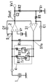
図8は本実施形態の焦電型赤外線検出装置の構成を示しており、参考例1のリミッタ回路4(図6参照)において、PMOSトランジスタTr1,Tr2に抵抗R11,R12を直列接続したもので、同様の構成には同一の符号を付して説明は省略する。
( Embodiment 2 )
FIG. 8 shows the configuration of the pyroelectric infrared detector of this embodiment. In the limiter circuit 4 (see FIG. 6) of Reference Example 1 , resistors R11 and R12 are connected in series to PMOS transistors Tr1 and Tr2. Similar components are denoted by the same reference numerals, and description thereof is omitted.
まず、抵抗R11,R12がないときに、演算増幅器2の反転入力端子Sinに1Hzと比べて非常に遅い周波数のゆらぎが入力された場合の動作について考える。この場合、演算増幅器2の出力端子Soutおよび直流帰還回路3の出力端子Sfoの電位もこのゆらぎに応答してゆらぎが発生するが、ゆらぎの振幅が大きいとリミッタ回路4が動作して、PMOSトランジスタTr1またはTr2がオンし、演算増幅器2の反転入力端子Sin−直流帰還回路3の出力端子Sfo間の抵抗値が急激に低下するため、出力端子Soutの出力波形に不連続が生じる。
First, let us consider an operation in the case where fluctuations of a very slow frequency compared with 1 Hz are input to the inverting input terminal Sin of the
ここで、人体検出の応用を考えた場合、人体の動きが1Hz付近を主成分とするために、後段に設けられる電圧増幅部(図示無し)においては、1Hz付近を中心に増幅する。したがって、1Hzと比べて非常に遅い周波数のゆらぎは後段の電圧増幅部で増幅されることはないので、誤報の原因となることはない。しかし、出力端子Soutの出力波形に不連続が生じると、不連続部分の変動には高周波成分が含まれるため、その高周波成分の1Hz付近の周波数成分が後段の電圧増幅部で増幅されて誤動作につながる。 Here, considering the application of human body detection, since the movement of the human body is mainly in the vicinity of 1 Hz, the voltage amplification unit (not shown) provided in the subsequent stage performs amplification around 1 Hz. Therefore, the fluctuation of the frequency that is very slow compared with 1 Hz is not amplified by the voltage amplification unit at the subsequent stage, so that it does not cause a false alarm. However, when a discontinuity occurs in the output waveform of the output terminal Sout, the fluctuation of the discontinuous portion includes a high-frequency component. Therefore, the frequency component in the vicinity of 1 Hz of the high-frequency component is amplified by the voltage amplification unit at the subsequent stage, resulting in malfunction. Connected.
そこで本実施形態では、PMOSトランジスタTr1,Tr2に直列接続された抵抗R11,R12によって、PMOSトランジスタTr1,Tr2が各々オンしたときに、演算増幅器2の反転入力端子Sin−直流帰還回路3の出力端子Sfo間の抵抗値が急激に低下することを抑制して、出力端子Soutの出力波形の不連続性を抑えている。したがって、出力端子Soutの出力波形の不連続性による誤動作を防止できる。
Therefore, in this embodiment, when the PMOS transistors Tr1 and Tr2 are turned on by the resistors R11 and R12 connected in series to the PMOS transistors Tr1 and Tr2, the inverting input terminal Sin of the
なお、本実施形態では参考例1のリミッタ回路4を例に説明したが、実施形態1,参考例2のリミッタ回路4の各PMOSトランジスタに抵抗を直列接続しても同様の効果を得ることができる。
In this embodiment, the
(実施形態3)
図9は本実施形態の焦電型赤外線検出装置の構成を示しており、実施形態1の図2とはリミッタ回路4の構成のみが異なるもので、同様の構成には同一の符号を付して説明は省略する。
( Embodiment 3 )
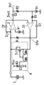
FIG. 9 shows the configuration of the pyroelectric infrared detection device of the present embodiment, which is different from FIG. 2 of the first embodiment only in the configuration of the
本実施形態のリミッタ回路4は、PMOSトランジスタTr1が入力抵抗Riに並列接続している。入力抵抗Riは一端を直流帰還回路3の出力端子Sfoに接続し、他端を演算増幅器2の反転入力端子Sinに接続しており、PMOSトランジスタTr1は、ドレイン端子を直流帰還回路3の出力端子Sfoに接続し、ソース端子、基板端子を反転入力端子Sinに接続している。PMOSトランジスタTr1のドレイン端子にはスイッチ素子SWA,SWBの直列回路の一端が接続され、スイッチ素子SWA,SWBの直列回路の他端は、抵抗R3とコンデンサC3との各一端同士の接続点に接続される。抵抗R3の他端は電源電位Vccに接続され、コンデンサC3の他端はグランドに接続される。PMOSトランジスタTr1のゲート端子は、スイッチ素子SWA,SWBの接続点に接続される。
In the
そして、電源投入直後は、スイッチ素子SWAはオフし、スイッチ素子SWBはオンする。スイッチ素子SWBがオンした直後はコンデンサC3には電荷が充電されていない状態であり、PMOSトランジスタTr1のゲート信号はLレベルであるので、PMOSトランジスタTr1のゲート−ソース間電圧Vgsがしきい値(負電圧)を超えて、PMOSトランジスタTr1がオンし、直流帰還回路3のコンデンサCfが急速に充電されて出力端子Soutの電位が急速に動作点に達する。その後、コンデンサC3が抵抗R3を介して電位Vccにまで充電されるにつれて、PMOSトランジスタTr1のゲート電位も上昇し、抵抗R3とコンデンサC3との時定数で決定される所定時間後にPMOSトランジスタTr1はオフする。
Immediately after the power is turned on, the switch element SWA is turned off and the switch element SWB is turned on. Immediately after the switch element SWB is turned on, the capacitor C3 is not charged, and the gate signal of the PMOS transistor Tr1 is at the L level. Therefore, the gate-source voltage Vgs of the PMOS transistor Tr1 is the threshold value ( The PMOS transistor Tr1 is turned on exceeding the negative voltage), the capacitor Cf of the
その後、スイッチ素子SWAがオン、スイッチ素子SWBがオフに切り換わり、PMOSトランジスタTr1のドレイン端子とゲート端子とがスイッチ素子SWAを介して接続される。そして、正の外来ノイズ印加時に、演算増幅器2の出力端子Soutおよび直流帰還回路3の出力端子Sfoの各電位が3Vまで上昇しようとすると、出力端子Sfoに接続したPMOSトランジスタTr1のドレイン電位も同様に上昇するので、PMOSトランジスタTr1のドレイン(P型)端子−基板(N型)端子間がダイオードとして導通する。入力抵抗Riの両端がPMOSトランジスタTr1によって短絡されると、端子Sout、Sfoの各電位はそれ以上上昇しなくなり、飽和することなく低下する。したがって、外来ノイズ印加後約1〜2秒後には入力信号に対して正常な応答を行う動作に復帰している。
Thereafter, the switch element SWA is turned on and the switch element SWB is turned off, and the drain terminal and the gate terminal of the PMOS transistor Tr1 are connected via the switch element SWA. When positive external noise is applied, if the potentials at the output terminal Sout of the
また、負の外来ノイズが印加されて、演算増幅器2の出力端子Soutおよび直流帰還回路3の出力端子Sfoの各電位が0Vまで下がろうとすると、出力端子Sfoにスイッチ素子SWAを介して接続したPMOSトランジスタTr1のゲート電位も同様に下がる。そして、端子Sout、Sfoの電位が1V付近まで下がると、PMOSトランジスタTr1のゲート−ソース間電圧Vgsがしきい値(負電圧)を超えて、PMOSトランジスタTr1がオンする。入力抵抗Riの両端がPMOSトランジスタTr1によって短絡されると、端子Sout、Sfoの各電位はそれ以上下がらなくなり、飽和することなく上昇する。したがって、外来ノイズ印加後約1〜2秒後には入力信号に対して正常な応答を行う動作に復帰している。
Further, when negative external noise is applied and each potential of the output terminal Sout of the
このように、電源投入時にコンデンサCfを急速に充電させるスタートアップ回路を備えることで電源投入から回路動作が安定するまでの時間をさらに短くすることができ、また、リミッタ回路4にスタートアップ回路を併用させることにより回路の小型化を図ることができる。
Thus, by providing the startup circuit that rapidly charges the capacitor Cf when the power is turned on, the time from when the power is turned on until the circuit operation is stabilized can be further shortened, and the
なお、実施形態1、参考例1,2においても、電源投入時にリミッタ回路4が備えるMOSトランジスタを所定期間導通させて、コンデンサCfを急速に充電させるスタートアップ回路を設ければ上記同様の効果を得ることができる。
In
また、実施形態1〜3、参考例1,2においてトランジスタTr1、Tr2はPMOSを用いているが、NMOSを用いてもよい。さらに、リミッタ回路4をトランジスタではなく、ダイオードで構成してもよい。
In the first to third embodiments and the reference examples 1 and 2 , the transistors Tr1 and Tr2 use PMOS. However, NMOS may be used. Further, the
1 焦電素子
2 演算増幅器
3 直流帰還回路
4 リミッタ回路
Cf 帰還容量
Ri 入力抵抗
Vr バイアス電位
Claims (2)
交流帰還回路を演算増幅器の出力端子−反転入力端子間に接続し、直流帰還回路の一端を演算増幅器の出力側に接続し、第1の抵抗素子を直流帰還回路の他端−演算増幅器の反転入力端子間に接続し、焦電素子を演算増幅器の反転入力端子に接続して、
リミッタ回路は、ソース端子を第1の抵抗素子の一端に接続し、ゲート端子、ドレイン端子を第1の抵抗素子の他端に接続した第1のMOSトランジスタと、ゲート端子、ドレイン端子を第1の抵抗素子の一端に接続し、ソース端子を第1の抵抗素子の他端に接続した第2のMOSトランジスタとから構成され、第1、第2のMOSトランジスタがP型の場合は各基板端子を電源電位に接続し、第1、第2のMOSトランジスタがN型の場合は各基板端子をグランドに接続し、
電源電位とグランドとの間に接続された第2の抵抗素子と第2のコンデンサとの直列回路と、第1,第2のMOSトランジスタのうち少なくともいずれか一方のMOSトランジスタのゲート端子とドレイン端子との間に接続された第1のスイッチ素子と、第2の抵抗素子および第2のコンデンサの接続中点と前記少なくともいずれか一方のMOSトランジスタのゲート端子との間に接続された第2のスイッチ素子を有して、電源投入後、第1のスイッチ素子がオフ、第2のスイッチ素子がオンして、前記少なくともいずれか一方のMOSトランジスタがオンし、第2のコンデンサの充電電圧によって前記少なくともいずれか一方のMOSトランジスタがオフした後、第1のスイッチ素子がオン、第2のスイッチ素子がオフすることによって、前記少なくともいずれか一方のMOSトランジスタを、電源投入時に所定期間導通させる
ことを特徴とする焦電型赤外線検出装置。 It is composed of a pyroelectric element that generates a current signal when sensing heat rays, an AC feedback circuit composed of a first capacitor, and an operational amplifier in which a series circuit of a DC feedback circuit and a first resistance element is connected between the input and output. A current-voltage conversion circuit that converts the current signal into a voltage signal and outputs the voltage signal;
The AC feedback circuit is connected between the output terminal and the inverting input terminal of the operational amplifier, one end of the DC feedback circuit is connected to the output side of the operational amplifier, and the first resistance element is connected to the other end of the DC feedback circuit and the inverse of the operational amplifier. Connect between the input terminals, connect the pyroelectric element to the inverting input terminal of the operational amplifier,
The limiter circuit includes a first MOS transistor having a source terminal connected to one end of the first resistance element, a gate terminal and a drain terminal connected to the other end of the first resistance element, and a gate terminal and a drain terminal connected to the first resistance element. And a second MOS transistor having a source terminal connected to the other end of the first resistor element, and each substrate terminal when the first and second MOS transistors are P-type. Is connected to the power supply potential, and when the first and second MOS transistors are N-type, each substrate terminal is connected to the ground ,
A series circuit of a second resistor and a second capacitor connected between the power supply potential and the ground, and a gate terminal and a drain terminal of at least one of the first and second MOS transistors A second switching element connected between a first switching element connected between the first switching element, a connection middle point of the second resistance element and the second capacitor, and a gate terminal of the at least one of the MOS transistors. Having a switch element, after turning on the power, the first switch element is turned off, the second switch element is turned on, the at least one MOS transistor is turned on, and the charge voltage of the second capacitor After at least one of the MOS transistors is turned off, the first switch element is turned on and the second switch element is turned off. Serial at least one of the MOS transistors, a pyroelectric infrared detection device, characterized in that for a predetermined period conductive when power is turned on.
Priority Applications (1)
| Application Number | Priority Date | Filing Date | Title |
|---|---|---|---|
| JP2004341072A JP4797366B2 (en) | 2004-11-25 | 2004-11-25 | Pyroelectric infrared detector |
Applications Claiming Priority (1)
| Application Number | Priority Date | Filing Date | Title |
|---|---|---|---|
| JP2004341072A JP4797366B2 (en) | 2004-11-25 | 2004-11-25 | Pyroelectric infrared detector |
Related Child Applications (1)
| Application Number | Title | Priority Date | Filing Date |
|---|---|---|---|
| JP2011069374A Division JP5685727B2 (en) | 2011-03-28 | 2011-03-28 | Infrared detection type human body detection device |
Publications (2)
| Publication Number | Publication Date |
|---|---|
| JP2006153510A JP2006153510A (en) | 2006-06-15 |
| JP4797366B2 true JP4797366B2 (en) | 2011-10-19 |
Family
ID=36632011
Family Applications (1)
| Application Number | Title | Priority Date | Filing Date |
|---|---|---|---|
| JP2004341072A Expired - Fee Related JP4797366B2 (en) | 2004-11-25 | 2004-11-25 | Pyroelectric infrared detector |
Country Status (1)
| Country | Link |
|---|---|
| JP (1) | JP4797366B2 (en) |
Families Citing this family (2)
| Publication number | Priority date | Publication date | Assignee | Title |
|---|---|---|---|---|
| JP5357733B2 (en) * | 2009-12-17 | 2013-12-04 | パナソニック株式会社 | Infrared gas detector |
| CN112510362B (en) * | 2020-09-25 | 2025-07-18 | 深圳迈睿智能科技有限公司 | Inverted double-feed type microwave detection module |
Family Cites Families (4)
| Publication number | Priority date | Publication date | Assignee | Title |
|---|---|---|---|---|
| JPS62145595A (en) * | 1985-12-20 | 1987-06-29 | Toshiba Corp | Semiconductor memory device |
| JPH0581670U (en) * | 1992-04-13 | 1993-11-05 | オプテックス株式会社 | Infrared detector |
| JP3374710B2 (en) * | 1996-10-30 | 2003-02-10 | 松下電工株式会社 | Feedback amplifier circuit |
| JP3557838B2 (en) * | 1997-03-26 | 2004-08-25 | 松下電工株式会社 | Pyroelectric infrared detector |
-
2004
- 2004-11-25 JP JP2004341072A patent/JP4797366B2/en not_active Expired - Fee Related
Also Published As
| Publication number | Publication date |
|---|---|
| JP2006153510A (en) | 2006-06-15 |
Similar Documents
| Publication | Publication Date | Title |
|---|---|---|
| US6882213B2 (en) | Temperature detection circuit insensitive to power supply voltage and temperature variation | |
| US6815685B2 (en) | Photodetector and method for detecting radiation | |
| US8147131B2 (en) | Temperature sensing circuit and electronic device using same | |
| US7129487B2 (en) | Infrared detecting circuit and an infrared detector | |
| US7535208B2 (en) | Capacitive feedback circuit | |
| US8723097B2 (en) | Illuminance sensor having light-level-independent consumption current | |
| JPH0581900A (en) | Stress mode sensing device for semiconductor memory device | |
| AU2005234374B2 (en) | Transconductance circuit for piezoelectric transducer | |
| US7141910B2 (en) | Transconductance circuit for piezoelectric transducer | |
| JP4797366B2 (en) | Pyroelectric infrared detector | |
| CN100367668C (en) | Semiconductor integrated circuit device | |
| JP5685727B2 (en) | Infrared detection type human body detection device | |
| US9983068B2 (en) | Overheat detection circuit and semiconductor device | |
| JP5517411B2 (en) | Infrared sensor and infrared solid-state imaging device | |
| JP3736026B2 (en) | Current-voltage conversion circuit in pyroelectric infrared detector | |
| US9825189B2 (en) | Dual-mode photosensitive pixel with gain stage | |
| JP4581629B2 (en) | Infrared detector | |
| JP2002185298A (en) | Physical quantity detection circuit | |
| JP3557838B2 (en) | Pyroelectric infrared detector | |
| JP5645247B2 (en) | Infrared detector | |
| JP5644519B2 (en) | Semiconductor integrated circuit | |
| JP2893738B2 (en) | Voltage detection circuit | |
| KR100368068B1 (en) | Assistant Circuit of Infrared Sensor Using Pyroeletric Effect | |
| CN104422528A (en) | Infrared detection device | |
| KR100844162B1 (en) | Photodiode Connection Circuit |
Legal Events
| Date | Code | Title | Description |
|---|---|---|---|
| A621 | Written request for application examination |
Free format text: JAPANESE INTERMEDIATE CODE: A621 Effective date: 20070518 |
|
| A977 | Report on retrieval |
Free format text: JAPANESE INTERMEDIATE CODE: A971007 Effective date: 20090421 |
|
| A131 | Notification of reasons for refusal |
Free format text: JAPANESE INTERMEDIATE CODE: A131 Effective date: 20091006 |
|
| A521 | Written amendment |
Free format text: JAPANESE INTERMEDIATE CODE: A523 Effective date: 20091207 |
|
| A131 | Notification of reasons for refusal |
Free format text: JAPANESE INTERMEDIATE CODE: A131 Effective date: 20100608 |
|
| RD04 | Notification of resignation of power of attorney |
Free format text: JAPANESE INTERMEDIATE CODE: A7424 Effective date: 20100809 |
|
| A02 | Decision of refusal |
Free format text: JAPANESE INTERMEDIATE CODE: A02 Effective date: 20101228 |
|
| A521 | Written amendment |
Free format text: JAPANESE INTERMEDIATE CODE: A523 Effective date: 20110328 |
|
| A911 | Transfer to examiner for re-examination before appeal (zenchi) |
Free format text: JAPANESE INTERMEDIATE CODE: A911 Effective date: 20110331 |
|
| TRDD | Decision of grant or rejection written | ||
| A01 | Written decision to grant a patent or to grant a registration (utility model) |
Free format text: JAPANESE INTERMEDIATE CODE: A01 Effective date: 20110705 |
|
| A01 | Written decision to grant a patent or to grant a registration (utility model) |
Free format text: JAPANESE INTERMEDIATE CODE: A01 |
|
| A61 | First payment of annual fees (during grant procedure) |
Free format text: JAPANESE INTERMEDIATE CODE: A61 Effective date: 20110718 |
|
| FPAY | Renewal fee payment (event date is renewal date of database) |
Free format text: PAYMENT UNTIL: 20140812 Year of fee payment: 3 |
|
| FPAY | Renewal fee payment (event date is renewal date of database) |
Free format text: PAYMENT UNTIL: 20140812 Year of fee payment: 3 |
|
| LAPS | Cancellation because of no payment of annual fees |