JP4797366B2 - 焦電型赤外線検出装置 - Google Patents
焦電型赤外線検出装置 Download PDFInfo
- Publication number
- JP4797366B2 JP4797366B2 JP2004341072A JP2004341072A JP4797366B2 JP 4797366 B2 JP4797366 B2 JP 4797366B2 JP 2004341072 A JP2004341072 A JP 2004341072A JP 2004341072 A JP2004341072 A JP 2004341072A JP 4797366 B2 JP4797366 B2 JP 4797366B2
- Authority
- JP
- Japan
- Prior art keywords
- terminal
- circuit
- operational amplifier
- turned
- feedback circuit
- Prior art date
- Legal status (The legal status is an assumption and is not a legal conclusion. Google has not performed a legal analysis and makes no representation as to the accuracy of the status listed.)
- Expired - Fee Related
Links
Images





Landscapes
- Radiation Pyrometers (AREA)
- Photometry And Measurement Of Optical Pulse Characteristics (AREA)
Description
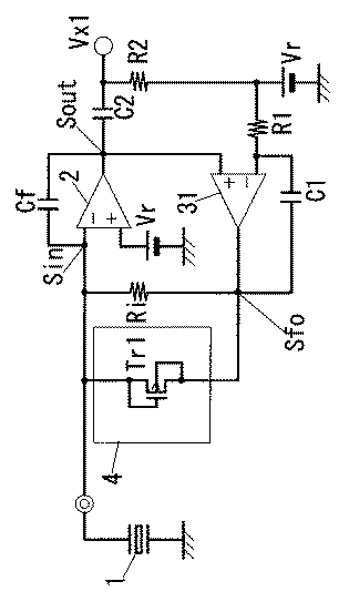
本発明の焦電型赤外線検出装置の基本構成は図1に示されるように、図10に示す従来例における入力抵抗Riにリミッタ回路4を並列接続したものであり、他の構成は図10と同様であり、同様の構成には同一の符号を付して説明は省略する。
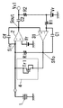
図6は本参考例の焦電型赤外線検出装置の構成を示しており、実施形態1の図2とはリミッタ回路4の構成のみが異なるもので、同様の構成には同一の符号を付して説明は省略する。
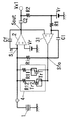
図7は本参考例の焦電型赤外線検出装置の構成を示しており、実施形態1の図2とはリミッタ回路4の構成のみが異なるもので、同様の構成には同一の符号を付して説明は省略する。
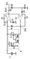
図8は本実施形態の焦電型赤外線検出装置の構成を示しており、参考例1のリミッタ回路4(図6参照)において、PMOSトランジスタTr1,Tr2に抵抗R11,R12を直列接続したもので、同様の構成には同一の符号を付して説明は省略する。
図9は本実施形態の焦電型赤外線検出装置の構成を示しており、実施形態1の図2とはリミッタ回路4の構成のみが異なるもので、同様の構成には同一の符号を付して説明は省略する。
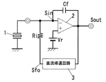
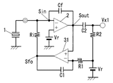
2 演算増幅器
3 直流帰還回路
4 リミッタ回路
Cf 帰還容量
Ri 入力抵抗
Vr バイアス電位
Claims (2)
- 熱線感知時に電流信号を発生する焦電素子と、第1のコンデンサからなる交流帰還回路、および直流帰還回路と第1の抵抗素子との直列回路を入出力間に接続した演算増幅器で構成されて前記電流信号を電圧信号に変換して出力する電流電圧変換回路とを備え、
交流帰還回路を演算増幅器の出力端子−反転入力端子間に接続し、直流帰還回路の一端を演算増幅器の出力側に接続し、第1の抵抗素子を直流帰還回路の他端−演算増幅器の反転入力端子間に接続し、焦電素子を演算増幅器の反転入力端子に接続して、
リミッタ回路は、ソース端子を第1の抵抗素子の一端に接続し、ゲート端子、ドレイン端子を第1の抵抗素子の他端に接続した第1のMOSトランジスタと、ゲート端子、ドレイン端子を第1の抵抗素子の一端に接続し、ソース端子を第1の抵抗素子の他端に接続した第2のMOSトランジスタとから構成され、第1、第2のMOSトランジスタがP型の場合は各基板端子を電源電位に接続し、第1、第2のMOSトランジスタがN型の場合は各基板端子をグランドに接続し、
電源電位とグランドとの間に接続された第2の抵抗素子と第2のコンデンサとの直列回路と、第1,第2のMOSトランジスタのうち少なくともいずれか一方のMOSトランジスタのゲート端子とドレイン端子との間に接続された第1のスイッチ素子と、第2の抵抗素子および第2のコンデンサの接続中点と前記少なくともいずれか一方のMOSトランジスタのゲート端子との間に接続された第2のスイッチ素子を有して、電源投入後、第1のスイッチ素子がオフ、第2のスイッチ素子がオンして、前記少なくともいずれか一方のMOSトランジスタがオンし、第2のコンデンサの充電電圧によって前記少なくともいずれか一方のMOSトランジスタがオフした後、第1のスイッチ素子がオン、第2のスイッチ素子がオフすることによって、前記少なくともいずれか一方のMOSトランジスタを、電源投入時に所定期間導通させる
ことを特徴とする焦電型赤外線検出装置。 - 前記リミッタ回路の各MOSトランジスタに第3の抵抗素子を各々直列接続したことを特徴とする請求項1記載の焦電型赤外線検出装置。
Priority Applications (1)
| Application Number | Priority Date | Filing Date | Title |
|---|---|---|---|
| JP2004341072A JP4797366B2 (ja) | 2004-11-25 | 2004-11-25 | 焦電型赤外線検出装置 |
Applications Claiming Priority (1)
| Application Number | Priority Date | Filing Date | Title |
|---|---|---|---|
| JP2004341072A JP4797366B2 (ja) | 2004-11-25 | 2004-11-25 | 焦電型赤外線検出装置 |
Related Child Applications (1)
| Application Number | Title | Priority Date | Filing Date |
|---|---|---|---|
| JP2011069374A Division JP5685727B2 (ja) | 2011-03-28 | 2011-03-28 | 赤外線検出型人体検知装置 |
Publications (2)
| Publication Number | Publication Date |
|---|---|
| JP2006153510A JP2006153510A (ja) | 2006-06-15 |
| JP4797366B2 true JP4797366B2 (ja) | 2011-10-19 |
Family
ID=36632011
Family Applications (1)
| Application Number | Title | Priority Date | Filing Date |
|---|---|---|---|
| JP2004341072A Expired - Fee Related JP4797366B2 (ja) | 2004-11-25 | 2004-11-25 | 焦電型赤外線検出装置 |
Country Status (1)
| Country | Link |
|---|---|
| JP (1) | JP4797366B2 (ja) |
Families Citing this family (2)
| Publication number | Priority date | Publication date | Assignee | Title |
|---|---|---|---|---|
| JP5357733B2 (ja) * | 2009-12-17 | 2013-12-04 | パナソニック株式会社 | 赤外線式ガス検知器 |
| CN112510362B (zh) * | 2020-09-25 | 2025-07-18 | 深圳迈睿智能科技有限公司 | 反相双馈电式微波探测模块 |
Family Cites Families (4)
| Publication number | Priority date | Publication date | Assignee | Title |
|---|---|---|---|---|
| JPS62145595A (ja) * | 1985-12-20 | 1987-06-29 | Toshiba Corp | 半導体記憶装置 |
| JPH0581670U (ja) * | 1992-04-13 | 1993-11-05 | オプテックス株式会社 | 赤外線式検知装置 |
| JP3374710B2 (ja) * | 1996-10-30 | 2003-02-10 | 松下電工株式会社 | 帰還増幅回路 |
| JP3557838B2 (ja) * | 1997-03-26 | 2004-08-25 | 松下電工株式会社 | 焦電型赤外線検出装置 |
-
2004
- 2004-11-25 JP JP2004341072A patent/JP4797366B2/ja not_active Expired - Fee Related
Also Published As
| Publication number | Publication date |
|---|---|
| JP2006153510A (ja) | 2006-06-15 |
Similar Documents
| Publication | Publication Date | Title |
|---|---|---|
| US6882213B2 (en) | Temperature detection circuit insensitive to power supply voltage and temperature variation | |
| US6815685B2 (en) | Photodetector and method for detecting radiation | |
| US8147131B2 (en) | Temperature sensing circuit and electronic device using same | |
| US7129487B2 (en) | Infrared detecting circuit and an infrared detector | |
| US7535208B2 (en) | Capacitive feedback circuit | |
| US8723097B2 (en) | Illuminance sensor having light-level-independent consumption current | |
| JPH0581900A (ja) | 半導体メモリー装置のストレスモード感知装置 | |
| AU2005234374B2 (en) | Transconductance circuit for piezoelectric transducer | |
| US7141910B2 (en) | Transconductance circuit for piezoelectric transducer | |
| JP4797366B2 (ja) | 焦電型赤外線検出装置 | |
| CN100367668C (zh) | 半导体集成电路器件 | |
| JP5685727B2 (ja) | 赤外線検出型人体検知装置 | |
| US9983068B2 (en) | Overheat detection circuit and semiconductor device | |
| JP5517411B2 (ja) | 赤外線センサ、及び赤外線固体撮像装置 | |
| JP3736026B2 (ja) | 焦電型赤外線検出装置における電流電圧変換回路 | |
| US9825189B2 (en) | Dual-mode photosensitive pixel with gain stage | |
| JP4581629B2 (ja) | 赤外線検知装置 | |
| JP2002185298A (ja) | 物理量検出回路 | |
| JP3557838B2 (ja) | 焦電型赤外線検出装置 | |
| JP5645247B2 (ja) | 赤外線検知装置 | |
| JP5644519B2 (ja) | 半導体集積回路 | |
| JP2893738B2 (ja) | 電圧検出回路 | |
| KR100368068B1 (ko) | 초전형 적외선 센서의 주변회로 장치 | |
| CN104422528A (zh) | 红外线检测装置 | |
| KR100844162B1 (ko) | 포토다이오드 연결회로 |
Legal Events
| Date | Code | Title | Description |
|---|---|---|---|
| A621 | Written request for application examination |
Free format text: JAPANESE INTERMEDIATE CODE: A621 Effective date: 20070518 |
|
| A977 | Report on retrieval |
Free format text: JAPANESE INTERMEDIATE CODE: A971007 Effective date: 20090421 |
|
| A131 | Notification of reasons for refusal |
Free format text: JAPANESE INTERMEDIATE CODE: A131 Effective date: 20091006 |
|
| A521 | Written amendment |
Free format text: JAPANESE INTERMEDIATE CODE: A523 Effective date: 20091207 |
|
| A131 | Notification of reasons for refusal |
Free format text: JAPANESE INTERMEDIATE CODE: A131 Effective date: 20100608 |
|
| RD04 | Notification of resignation of power of attorney |
Free format text: JAPANESE INTERMEDIATE CODE: A7424 Effective date: 20100809 |
|
| A02 | Decision of refusal |
Free format text: JAPANESE INTERMEDIATE CODE: A02 Effective date: 20101228 |
|
| A521 | Written amendment |
Free format text: JAPANESE INTERMEDIATE CODE: A523 Effective date: 20110328 |
|
| A911 | Transfer to examiner for re-examination before appeal (zenchi) |
Free format text: JAPANESE INTERMEDIATE CODE: A911 Effective date: 20110331 |
|
| TRDD | Decision of grant or rejection written | ||
| A01 | Written decision to grant a patent or to grant a registration (utility model) |
Free format text: JAPANESE INTERMEDIATE CODE: A01 Effective date: 20110705 |
|
| A01 | Written decision to grant a patent or to grant a registration (utility model) |
Free format text: JAPANESE INTERMEDIATE CODE: A01 |
|
| A61 | First payment of annual fees (during grant procedure) |
Free format text: JAPANESE INTERMEDIATE CODE: A61 Effective date: 20110718 |
|
| FPAY | Renewal fee payment (event date is renewal date of database) |
Free format text: PAYMENT UNTIL: 20140812 Year of fee payment: 3 |
|
| FPAY | Renewal fee payment (event date is renewal date of database) |
Free format text: PAYMENT UNTIL: 20140812 Year of fee payment: 3 |
|
| LAPS | Cancellation because of no payment of annual fees |