JP4803993B2 - 半導体装置の製造方法 - Google Patents
半導体装置の製造方法 Download PDFInfo
- Publication number
- JP4803993B2 JP4803993B2 JP2004325035A JP2004325035A JP4803993B2 JP 4803993 B2 JP4803993 B2 JP 4803993B2 JP 2004325035 A JP2004325035 A JP 2004325035A JP 2004325035 A JP2004325035 A JP 2004325035A JP 4803993 B2 JP4803993 B2 JP 4803993B2
- Authority
- JP
- Japan
- Prior art keywords
- substrate
- semiconductor device
- conductive portion
- manufacturing
- insulating film
- Prior art date
- Legal status (The legal status is an assumption and is not a legal conclusion. Google has not performed a legal analysis and makes no representation as to the accuracy of the status listed.)
- Expired - Lifetime
Links
Images























Classifications
-
- H—ELECTRICITY
- H10—SEMICONDUCTOR DEVICES; ELECTRIC SOLID-STATE DEVICES NOT OTHERWISE PROVIDED FOR
- H10W—GENERIC PACKAGES, INTERCONNECTIONS, CONNECTORS OR OTHER CONSTRUCTIONAL DETAILS OF DEVICES COVERED BY CLASS H10
- H10W20/00—Interconnections in chips, wafers or substrates
- H10W20/01—Manufacture or treatment
- H10W20/021—Manufacture or treatment of interconnections within wafers or substrates
- H10W20/023—Manufacture or treatment of interconnections within wafers or substrates the interconnections being through-semiconductor vias
-
- H—ELECTRICITY
- H10—SEMICONDUCTOR DEVICES; ELECTRIC SOLID-STATE DEVICES NOT OTHERWISE PROVIDED FOR
- H10W—GENERIC PACKAGES, INTERCONNECTIONS, CONNECTORS OR OTHER CONSTRUCTIONAL DETAILS OF DEVICES COVERED BY CLASS H10
- H10W72/00—Interconnections or connectors in packages
-
- H—ELECTRICITY
- H10—SEMICONDUCTOR DEVICES; ELECTRIC SOLID-STATE DEVICES NOT OTHERWISE PROVIDED FOR
- H10D—INORGANIC ELECTRIC SEMICONDUCTOR DEVICES
- H10D62/00—Semiconductor bodies, or regions thereof, of devices having potential barriers
- H10D62/10—Shapes, relative sizes or dispositions of the regions of the semiconductor bodies; Shapes of the semiconductor bodies
- H10D62/117—Shapes of semiconductor bodies
-
- H—ELECTRICITY
- H10—SEMICONDUCTOR DEVICES; ELECTRIC SOLID-STATE DEVICES NOT OTHERWISE PROVIDED FOR
- H10P—GENERIC PROCESSES OR APPARATUS FOR THE MANUFACTURE OR TREATMENT OF DEVICES COVERED BY CLASS H10
- H10P72/00—Handling or holding of wafers, substrates or devices during manufacture or treatment thereof
- H10P72/70—Handling or holding of wafers, substrates or devices during manufacture or treatment thereof for supporting or gripping
- H10P72/74—Handling or holding of wafers, substrates or devices during manufacture or treatment thereof for supporting or gripping using temporarily an auxiliary support
-
- H—ELECTRICITY
- H10—SEMICONDUCTOR DEVICES; ELECTRIC SOLID-STATE DEVICES NOT OTHERWISE PROVIDED FOR
- H10W—GENERIC PACKAGES, INTERCONNECTIONS, CONNECTORS OR OTHER CONSTRUCTIONAL DETAILS OF DEVICES COVERED BY CLASS H10
- H10W20/00—Interconnections in chips, wafers or substrates
- H10W20/01—Manufacture or treatment
- H10W20/021—Manufacture or treatment of interconnections within wafers or substrates
- H10W20/023—Manufacture or treatment of interconnections within wafers or substrates the interconnections being through-semiconductor vias
- H10W20/0245—Manufacture or treatment of interconnections within wafers or substrates the interconnections being through-semiconductor vias comprising use of blind vias during the manufacture
-
- H—ELECTRICITY
- H10—SEMICONDUCTOR DEVICES; ELECTRIC SOLID-STATE DEVICES NOT OTHERWISE PROVIDED FOR
- H10W—GENERIC PACKAGES, INTERCONNECTIONS, CONNECTORS OR OTHER CONSTRUCTIONAL DETAILS OF DEVICES COVERED BY CLASS H10
- H10W20/00—Interconnections in chips, wafers or substrates
- H10W20/01—Manufacture or treatment
- H10W20/021—Manufacture or treatment of interconnections within wafers or substrates
- H10W20/023—Manufacture or treatment of interconnections within wafers or substrates the interconnections being through-semiconductor vias
- H10W20/0261—Manufacture or treatment of interconnections within wafers or substrates the interconnections being through-semiconductor vias characterised by the filling method or the material of the conductive fill
-
- H—ELECTRICITY
- H10—SEMICONDUCTOR DEVICES; ELECTRIC SOLID-STATE DEVICES NOT OTHERWISE PROVIDED FOR
- H10W—GENERIC PACKAGES, INTERCONNECTIONS, CONNECTORS OR OTHER CONSTRUCTIONAL DETAILS OF DEVICES COVERED BY CLASS H10
- H10W20/00—Interconnections in chips, wafers or substrates
- H10W20/01—Manufacture or treatment
- H10W20/021—Manufacture or treatment of interconnections within wafers or substrates
- H10W20/023—Manufacture or treatment of interconnections within wafers or substrates the interconnections being through-semiconductor vias
- H10W20/0265—Manufacture or treatment of interconnections within wafers or substrates the interconnections being through-semiconductor vias characterised by the sidewall insulation
-
- H—ELECTRICITY
- H10—SEMICONDUCTOR DEVICES; ELECTRIC SOLID-STATE DEVICES NOT OTHERWISE PROVIDED FOR
- H10W—GENERIC PACKAGES, INTERCONNECTIONS, CONNECTORS OR OTHER CONSTRUCTIONAL DETAILS OF DEVICES COVERED BY CLASS H10
- H10W20/00—Interconnections in chips, wafers or substrates
- H10W20/20—Interconnections within wafers or substrates, e.g. through-silicon vias [TSV]
-
- H—ELECTRICITY
- H10—SEMICONDUCTOR DEVICES; ELECTRIC SOLID-STATE DEVICES NOT OTHERWISE PROVIDED FOR
- H10W—GENERIC PACKAGES, INTERCONNECTIONS, CONNECTORS OR OTHER CONSTRUCTIONAL DETAILS OF DEVICES COVERED BY CLASS H10
- H10W70/00—Package substrates; Interposers; Redistribution layers [RDL]
- H10W70/01—Manufacture or treatment
- H10W70/05—Manufacture or treatment of insulating or insulated package substrates, or of interposers, or of redistribution layers
- H10W70/093—Connecting or disconnecting other interconnections thereto or therefrom, e.g. connecting bond wires or bumps
-
- H—ELECTRICITY
- H10—SEMICONDUCTOR DEVICES; ELECTRIC SOLID-STATE DEVICES NOT OTHERWISE PROVIDED FOR
- H10W—GENERIC PACKAGES, INTERCONNECTIONS, CONNECTORS OR OTHER CONSTRUCTIONAL DETAILS OF DEVICES COVERED BY CLASS H10
- H10W90/00—Package configurations
-
- H—ELECTRICITY
- H10—SEMICONDUCTOR DEVICES; ELECTRIC SOLID-STATE DEVICES NOT OTHERWISE PROVIDED FOR
- H10P—GENERIC PROCESSES OR APPARATUS FOR THE MANUFACTURE OR TREATMENT OF DEVICES COVERED BY CLASS H10
- H10P72/00—Handling or holding of wafers, substrates or devices during manufacture or treatment thereof
- H10P72/70—Handling or holding of wafers, substrates or devices during manufacture or treatment thereof for supporting or gripping
- H10P72/74—Handling or holding of wafers, substrates or devices during manufacture or treatment thereof for supporting or gripping using temporarily an auxiliary support
- H10P72/7422—Handling or holding of wafers, substrates or devices during manufacture or treatment thereof for supporting or gripping using temporarily an auxiliary support used to protect an active side of a device or wafer
-
- H—ELECTRICITY
- H10—SEMICONDUCTOR DEVICES; ELECTRIC SOLID-STATE DEVICES NOT OTHERWISE PROVIDED FOR
- H10P—GENERIC PROCESSES OR APPARATUS FOR THE MANUFACTURE OR TREATMENT OF DEVICES COVERED BY CLASS H10
- H10P72/00—Handling or holding of wafers, substrates or devices during manufacture or treatment thereof
- H10P72/70—Handling or holding of wafers, substrates or devices during manufacture or treatment thereof for supporting or gripping
- H10P72/74—Handling or holding of wafers, substrates or devices during manufacture or treatment thereof for supporting or gripping using temporarily an auxiliary support
- H10P72/7432—Handling or holding of wafers, substrates or devices during manufacture or treatment thereof for supporting or gripping using temporarily an auxiliary support used in a transfer process involving transfer directly from an origin substrate to a target substrate without use of an intermediate handle substrate
-
- H—ELECTRICITY
- H10—SEMICONDUCTOR DEVICES; ELECTRIC SOLID-STATE DEVICES NOT OTHERWISE PROVIDED FOR
- H10W—GENERIC PACKAGES, INTERCONNECTIONS, CONNECTORS OR OTHER CONSTRUCTIONAL DETAILS OF DEVICES COVERED BY CLASS H10
- H10W70/00—Package substrates; Interposers; Redistribution layers [RDL]
- H10W70/60—Insulating or insulated package substrates; Interposers; Redistribution layers
-
- H—ELECTRICITY
- H10—SEMICONDUCTOR DEVICES; ELECTRIC SOLID-STATE DEVICES NOT OTHERWISE PROVIDED FOR
- H10W—GENERIC PACKAGES, INTERCONNECTIONS, CONNECTORS OR OTHER CONSTRUCTIONAL DETAILS OF DEVICES COVERED BY CLASS H10
- H10W72/00—Interconnections or connectors in packages
- H10W72/01—Manufacture or treatment
- H10W72/012—Manufacture or treatment of bump connectors, dummy bumps or thermal bumps
- H10W72/01251—Changing the shapes of bumps
- H10W72/01255—Changing the shapes of bumps by using masks
-
- H—ELECTRICITY
- H10—SEMICONDUCTOR DEVICES; ELECTRIC SOLID-STATE DEVICES NOT OTHERWISE PROVIDED FOR
- H10W—GENERIC PACKAGES, INTERCONNECTIONS, CONNECTORS OR OTHER CONSTRUCTIONAL DETAILS OF DEVICES COVERED BY CLASS H10
- H10W72/00—Interconnections or connectors in packages
- H10W72/071—Connecting or disconnecting
- H10W72/072—Connecting or disconnecting of bump connectors
- H10W72/07251—Connecting or disconnecting of bump connectors characterised by changes in properties of the bump connectors during connecting
-
- H—ELECTRICITY
- H10—SEMICONDUCTOR DEVICES; ELECTRIC SOLID-STATE DEVICES NOT OTHERWISE PROVIDED FOR
- H10W—GENERIC PACKAGES, INTERCONNECTIONS, CONNECTORS OR OTHER CONSTRUCTIONAL DETAILS OF DEVICES COVERED BY CLASS H10
- H10W72/00—Interconnections or connectors in packages
- H10W72/20—Bump connectors, e.g. solder bumps or copper pillars; Dummy bumps; Thermal bumps
-
- H—ELECTRICITY
- H10—SEMICONDUCTOR DEVICES; ELECTRIC SOLID-STATE DEVICES NOT OTHERWISE PROVIDED FOR
- H10W—GENERIC PACKAGES, INTERCONNECTIONS, CONNECTORS OR OTHER CONSTRUCTIONAL DETAILS OF DEVICES COVERED BY CLASS H10
- H10W90/00—Package configurations
- H10W90/20—Configurations of stacked chips
- H10W90/297—Configurations of stacked chips characterised by the through-semiconductor vias [TSVs] in the stacked chips
-
- H—ELECTRICITY
- H10—SEMICONDUCTOR DEVICES; ELECTRIC SOLID-STATE DEVICES NOT OTHERWISE PROVIDED FOR
- H10W—GENERIC PACKAGES, INTERCONNECTIONS, CONNECTORS OR OTHER CONSTRUCTIONAL DETAILS OF DEVICES COVERED BY CLASS H10
- H10W90/00—Package configurations
- H10W90/701—Package configurations characterised by the relative positions of pads or connectors relative to package parts
- H10W90/721—Package configurations characterised by the relative positions of pads or connectors relative to package parts of bump connectors
- H10W90/722—Package configurations characterised by the relative positions of pads or connectors relative to package parts of bump connectors between stacked chips
Landscapes
- Internal Circuitry In Semiconductor Integrated Circuit Devices (AREA)
- Mechanical Treatment Of Semiconductor (AREA)
- Wire Bonding (AREA)
Description
い場合にも、微細化が可能であり、信頼性が高く、かつ、形成が容易な貫通電極を有する半導体装置およびその製造方法を提供することである。
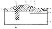
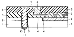
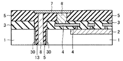
まず、図1を用いて実施の形態1の半導体装置の構造を説明する。
次に、実施の形態2の半導体装置の構造を図10を用いて説明する。
次に、図20〜図25を用いて、実施の形態3の半導体装置の構造を説明する。
次に、図26〜図31を用いて、本実施の形態の半導体装置の構造を説明する。
次に、実施の形態5の半導体装置を図32を用いて説明する。
次に、図49を用いて実施の形態6の半導体装置の構造を説明する。
次に、図57を用いて実施の形態7の半導体装置の構造を説明する。
次に、図59〜図65を用いて、実施の形態8の半導体装置の製造方法を説明する。
次に、図66〜図71を用いて、実施の形態9の半導体装置の製造方法を説明する。
次に、図72を用いて、実施の形態10の半導体装置の構造を説明する。
次に、図84を用いて実施の形態11の半導体装置の構造を説明する。
次に、図89〜図94を用いて実施の形態12の半導体装置の構造を説明する。
次に、実施の形態13の半導体装置の構造を説明する。
Claims (8)
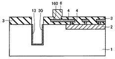
- 凹型基板と凸型基板とを準備するステップを備えた半導体装置の製造方法であって、
前記凹型基板は、
半導体回路を有する半導体基板と、
前記半導体回路を含む前記半導体基板の主表面を覆うように設けられた第1の絶縁膜と、
前記第1の絶縁膜内に設けられた内部配線とを含み、
前記第1の絶縁膜および前記半導体基板には、前記第1の絶縁膜および前記半導体基板の厚さ方向に延びる凹部が設けられており、
前記凸型基板は、
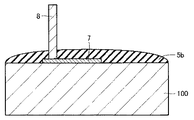
仮基板と、
前記仮基板上に形成された導電部と、
前記仮基板の主表面に対して垂直な方向に延びる柱状導電部とを含み、
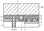
前記凸型基板および前記凹型基板のうちの少なくともいずれか一方の接合面において流動性を有する絶縁材が塗布された状態で、前記凹型基板と前記凸型基板とが嵌め合わされるか、または、前記凹型基板と前記凸型基板とが隙間を有する状態で嵌め合わされ、前記隙間に流動性を有する絶縁材が注入されるステップと、
前記導電部と前記内部配線とが直接的にまたは他の部材を介して電気的に接続されるステップと、
前記流動性を有する絶縁材を硬化させ、第2の絶縁膜を形成するステップと、
前記半導体基板の裏面を研磨することによって前記柱状導電部を露出させるステップと、
前記仮基板を除去することによって前記導電部を露出させるステップとをさらに備えた、半導体装置の製造方法。 - 前記凸型基板は、前記柱状導電部を複数含み、
前記凹型基板には、少なくとも1つの凹部が設けられており、
2以上の前記柱状導電部が前記1つの凹部内に挿入される、請求項1に記載の半導体装置の製造方法。 - 前記仮基板が導電性を有し、
前記凸型基板を準備するステップは、
前記仮基板の上に前記柱状導電部を形成するための型を形成するステップと、
前記仮基板を陰極として用いる電気めっきによって前記型の中に前記柱状導電部を形成するステップとを含む、請求項1に記載の半導体装置の製造方法。 - 前記柱状導電部の先端に突起電極を電気めっきにより形成するステップをさらに備えた、請求項1に記載の半導体装置の製造方法。
- 前記第2の絶縁膜の表面を覆う保護膜を形成するステップをさらに備えた、請求項1に記載の半導体装置の製造方法。
- 前記凸型基板および前記凹型基板のうちの少なくともいずれか一方の接合面において流動性を有する絶縁材が塗布された状態で、前記凹型基板と前記凸型基板とが嵌め合わされるか、または、前記凹型基板と前記凸型基板とが隙間を有する状態で嵌め合わされ、前記隙間に流動性を有する絶縁材が注入されるステップの前に、前記凹部の表面上に該表面に沿う導電膜を形成するステップをさらに備えた、請求項1に記載の半導体装置の製造方法。
- 前記内部配線は、前記導電部の下側において前記貫通電極を取り囲むように設けられ、かつ、前記導電部の下面に接触しており、
前記内部配線および前記導電部のうちの少なくともいずれか一方に切欠きが設けられており、
前記切欠きを介して前記絶縁材が流動する、請求項1に記載の半導体装置の製造方法。 - 前記凸型基板を準備するステップにおいて、前記柱状導電部の表面全体を覆うように第3の絶縁膜を形成するステップをさらに備えた、請求項1に記載の半導体装置の製造方法。
Priority Applications (5)
| Application Number | Priority Date | Filing Date | Title |
|---|---|---|---|
| JP2004325035A JP4803993B2 (ja) | 2004-11-09 | 2004-11-09 | 半導体装置の製造方法 |
| US11/088,952 US7288481B2 (en) | 2004-11-09 | 2005-03-25 | Semiconductor device having through electrode and method of manufacturing the same |
| TW094112209A TWI344668B (en) | 2004-11-09 | 2005-04-18 | Semiconductor device and method of manufacturing the same |
| DE102005025452.7A DE102005025452B4 (de) | 2004-11-09 | 2005-06-02 | Verfahren zur Herstellung einer Halbleitervorrichtung mit einer Durchgangselektrode |
| KR1020050059703A KR101161718B1 (ko) | 2004-11-09 | 2005-07-04 | 관통전극을 갖는 반도체 장치 및 그 제조 방법 |
Applications Claiming Priority (1)
| Application Number | Priority Date | Filing Date | Title |
|---|---|---|---|
| JP2004325035A JP4803993B2 (ja) | 2004-11-09 | 2004-11-09 | 半導体装置の製造方法 |
Publications (2)
| Publication Number | Publication Date |
|---|---|
| JP2006135233A JP2006135233A (ja) | 2006-05-25 |
| JP4803993B2 true JP4803993B2 (ja) | 2011-10-26 |
Family
ID=36217364
Family Applications (1)
| Application Number | Title | Priority Date | Filing Date |
|---|---|---|---|
| JP2004325035A Expired - Lifetime JP4803993B2 (ja) | 2004-11-09 | 2004-11-09 | 半導体装置の製造方法 |
Country Status (5)
| Country | Link |
|---|---|
| US (1) | US7288481B2 (ja) |
| JP (1) | JP4803993B2 (ja) |
| KR (1) | KR101161718B1 (ja) |
| DE (1) | DE102005025452B4 (ja) |
| TW (1) | TWI344668B (ja) |
Families Citing this family (18)
| Publication number | Priority date | Publication date | Assignee | Title |
|---|---|---|---|---|
| US8278738B2 (en) * | 2005-02-17 | 2012-10-02 | Sharp Kabushiki Kaisha | Method of producing semiconductor device and semiconductor device |
| US7772115B2 (en) * | 2005-09-01 | 2010-08-10 | Micron Technology, Inc. | Methods for forming through-wafer interconnects, intermediate structures so formed, and devices and systems having at least one solder dam structure |
| US7344959B1 (en) * | 2006-07-25 | 2008-03-18 | International Business Machines Corporation | Metal filled through via structure for providing vertical wafer-to-wafer interconnection |
| US7973413B2 (en) * | 2007-08-24 | 2011-07-05 | Taiwan Semiconductor Manufacturing Company, Ltd. | Through-substrate via for semiconductor device |
| JP2010114320A (ja) * | 2008-11-07 | 2010-05-20 | Panasonic Corp | 半導体装置 |
| US9142586B2 (en) * | 2009-02-24 | 2015-09-22 | Taiwan Semiconductor Manufacturing Company, Ltd. | Pad design for backside illuminated image sensor |
| US8531565B2 (en) * | 2009-02-24 | 2013-09-10 | Taiwan Semiconductor Manufacturing Company, Ltd. | Front side implanted guard ring structure for backside illuminated image sensor |
| JP5574639B2 (ja) * | 2009-08-21 | 2014-08-20 | 三菱電機株式会社 | 半導体装置およびその製造方法 |
| US8232137B2 (en) * | 2009-12-10 | 2012-07-31 | Intersil Americas Inc. | Heat conduction for chip stacks and 3-D circuits |
| US8492260B2 (en) | 2010-08-30 | 2013-07-23 | Semionductor Components Industries, LLC | Processes of forming an electronic device including a feature in a trench |
| KR101688006B1 (ko) * | 2010-11-26 | 2016-12-20 | 삼성전자주식회사 | 반도체 장치 |
| JP6051359B2 (ja) * | 2010-12-22 | 2016-12-27 | 俊 保坂 | コア付きインダクタ素子およびその製造方法 |
| KR101801137B1 (ko) * | 2011-02-21 | 2017-11-24 | 삼성전자주식회사 | 반도체 장치 및 그 제조 방법 |
| JP6154583B2 (ja) * | 2012-06-14 | 2017-06-28 | ラピスセミコンダクタ株式会社 | 半導体装置およびその製造方法 |
| US8981533B2 (en) | 2012-09-13 | 2015-03-17 | Semiconductor Components Industries, Llc | Electronic device including a via and a conductive structure, a process of forming the same, and an interposer |
| US9159699B2 (en) * | 2012-11-13 | 2015-10-13 | Delta Electronics, Inc. | Interconnection structure having a via structure |
| US9449898B2 (en) * | 2013-07-31 | 2016-09-20 | Taiwan Semiconductor Manufacturing Company, Ltd. | Semiconductor device having backside interconnect structure through substrate via and method of forming the same |
| US9812354B2 (en) | 2015-05-15 | 2017-11-07 | Semiconductor Components Industries, Llc | Process of forming an electronic device including a material defining a void |
Family Cites Families (6)
| Publication number | Priority date | Publication date | Assignee | Title |
|---|---|---|---|---|
| JPH01185943A (ja) * | 1988-01-21 | 1989-07-25 | Nec Corp | 半導体集積回路装置 |
| US5646067A (en) * | 1995-06-05 | 1997-07-08 | Harris Corporation | Method of bonding wafers having vias including conductive material |
| JP2001127242A (ja) * | 1999-10-22 | 2001-05-11 | Seiko Epson Corp | 半導体チップ、マルチチップパッケージ、半導体装置、並びに電子機器、およびそれらの製造方法 |
| JP4522574B2 (ja) | 2000-12-04 | 2010-08-11 | 大日本印刷株式会社 | 半導体装置の作製方法 |
| JP2004296896A (ja) * | 2003-03-27 | 2004-10-21 | Seiko Epson Corp | 半導体装置、半導体デバイス、電子機器、および半導体装置の製造方法 |
| JP2006080149A (ja) * | 2004-09-07 | 2006-03-23 | Sharp Corp | 半導体装置の積層構造 |
-
2004
- 2004-11-09 JP JP2004325035A patent/JP4803993B2/ja not_active Expired - Lifetime
-
2005
- 2005-03-25 US US11/088,952 patent/US7288481B2/en not_active Expired - Lifetime
- 2005-04-18 TW TW094112209A patent/TWI344668B/zh not_active IP Right Cessation
- 2005-06-02 DE DE102005025452.7A patent/DE102005025452B4/de not_active Expired - Lifetime
- 2005-07-04 KR KR1020050059703A patent/KR101161718B1/ko not_active Expired - Lifetime
Also Published As
| Publication number | Publication date |
|---|---|
| DE102005025452A1 (de) | 2006-05-11 |
| JP2006135233A (ja) | 2006-05-25 |
| TWI344668B (en) | 2011-07-01 |
| TW200616023A (en) | 2006-05-16 |
| US20060097357A1 (en) | 2006-05-11 |
| KR101161718B1 (ko) | 2012-07-03 |
| KR20060049816A (ko) | 2006-05-19 |
| DE102005025452B4 (de) | 2014-06-26 |
| US7288481B2 (en) | 2007-10-30 |
Similar Documents
| Publication | Publication Date | Title |
|---|---|---|
| JP4803993B2 (ja) | 半導体装置の製造方法 | |
| JP4327644B2 (ja) | 半導体装置の製造方法 | |
| JP6286169B2 (ja) | 配線基板及びその製造方法 | |
| US7745924B2 (en) | Capacitor embedded in interposer, semiconductor device including the same, and method for manufacturing capacitor embedded in interposer | |
| JP4439976B2 (ja) | 半導体装置およびその製造方法 | |
| JP4035034B2 (ja) | 半導体装置およびその製造方法 | |
| CN101916754B (zh) | 通孔和通孔形成方法以及通孔填充方法 | |
| JP2006135175A (ja) | 基板及びその製造方法 | |
| JP2008305897A (ja) | 半導体装置およびその製造方法 | |
| JP5423572B2 (ja) | 配線基板、圧電発振器、ジャイロセンサー、配線基板の製造方法 | |
| US7768132B2 (en) | Circuit device and manufacturing method thereof | |
| JP4713602B2 (ja) | 基板モジュールおよびその製造方法ならびに電子機器 | |
| TWI356479B (en) | Package structure with embedded die and method of | |
| US8723051B2 (en) | Wiring substrate and method for manufacturing wiring substrate | |
| CN112864105B (zh) | 感测装置的封装结构的制造方法 | |
| JP2004119773A (ja) | 半導体装置及びその製造方法 | |
| KR101139650B1 (ko) | 배선 기판, 그 제조 방법, 및 반도체 장치 | |
| JP2006261323A (ja) | 半導体装置及びその製造方法 | |
| JP4950012B2 (ja) | シリコンスルーホールを有する半導体チップ装置及びその製造方法 | |
| JP4764710B2 (ja) | 半導体装置とその製造方法 | |
| JP5980554B2 (ja) | 電気的接続部材、検査方法及び電気的接続部材の製造方法 | |
| JP2011238742A (ja) | 配線基板の製造方法及び配線基板 | |
| JP2005347476A (ja) | 回路装置の製造方法 | |
| JP6712136B2 (ja) | 電子部品の製造方法 | |
| JP7707681B2 (ja) | 配線基板 |
Legal Events
| Date | Code | Title | Description |
|---|---|---|---|
| A621 | Written request for application examination |
Free format text: JAPANESE INTERMEDIATE CODE: A621 Effective date: 20071016 |
|
| A977 | Report on retrieval |
Free format text: JAPANESE INTERMEDIATE CODE: A971007 Effective date: 20091130 |
|
| A711 | Notification of change in applicant |
Free format text: JAPANESE INTERMEDIATE CODE: A712 Effective date: 20100526 |
|
| A131 | Notification of reasons for refusal |
Free format text: JAPANESE INTERMEDIATE CODE: A131 Effective date: 20110524 |
|
| A521 | Request for written amendment filed |
Free format text: JAPANESE INTERMEDIATE CODE: A523 Effective date: 20110712 |
|
| TRDD | Decision of grant or rejection written | ||
| A01 | Written decision to grant a patent or to grant a registration (utility model) |
Free format text: JAPANESE INTERMEDIATE CODE: A01 Effective date: 20110802 |
|
| A01 | Written decision to grant a patent or to grant a registration (utility model) |
Free format text: JAPANESE INTERMEDIATE CODE: A01 |
|
| A61 | First payment of annual fees (during grant procedure) |
Free format text: JAPANESE INTERMEDIATE CODE: A61 Effective date: 20110809 |
|
| R150 | Certificate of patent or registration of utility model |
Free format text: JAPANESE INTERMEDIATE CODE: R150 Ref document number: 4803993 Country of ref document: JP Free format text: JAPANESE INTERMEDIATE CODE: R150 |
|
| FPAY | Renewal fee payment (event date is renewal date of database) |
Free format text: PAYMENT UNTIL: 20140819 Year of fee payment: 3 |
|
| S531 | Written request for registration of change of domicile |
Free format text: JAPANESE INTERMEDIATE CODE: R313531 |
|
| R350 | Written notification of registration of transfer |
Free format text: JAPANESE INTERMEDIATE CODE: R350 |
|
| EXPY | Cancellation because of completion of term |