JP4807931B2 - 狭いドーピング・プロファイルを有する高性能半導体デバイスを作成する構造および方法 - Google Patents
狭いドーピング・プロファイルを有する高性能半導体デバイスを作成する構造および方法 Download PDFInfo
- Publication number
- JP4807931B2 JP4807931B2 JP2003373787A JP2003373787A JP4807931B2 JP 4807931 B2 JP4807931 B2 JP 4807931B2 JP 2003373787 A JP2003373787 A JP 2003373787A JP 2003373787 A JP2003373787 A JP 2003373787A JP 4807931 B2 JP4807931 B2 JP 4807931B2
- Authority
- JP
- Japan
- Prior art keywords
- layer
- region
- intruder
- base
- heterojunction
- Prior art date
- Legal status (The legal status is an assumption and is not a legal conclusion. Google has not performed a legal analysis and makes no representation as to the accuracy of the status listed.)
- Expired - Fee Related
Links
- 239000004065 semiconductor Substances 0.000 title claims description 33
- 238000000034 method Methods 0.000 title claims description 14
- 239000000463 material Substances 0.000 claims description 33
- 229910000577 Silicon-germanium Inorganic materials 0.000 claims description 22
- XUIMIQQOPSSXEZ-UHFFFAOYSA-N Silicon Chemical group [Si] XUIMIQQOPSSXEZ-UHFFFAOYSA-N 0.000 claims description 20
- 229910052710 silicon Inorganic materials 0.000 claims description 20
- 239000010703 silicon Substances 0.000 claims description 20
- OKTJSMMVPCPJKN-UHFFFAOYSA-N Carbon Chemical compound [C] OKTJSMMVPCPJKN-UHFFFAOYSA-N 0.000 claims description 17
- 229910052799 carbon Inorganic materials 0.000 claims description 17
- 239000002019 doping agent Substances 0.000 claims description 13
- 239000000758 substrate Substances 0.000 claims description 11
- 230000015572 biosynthetic process Effects 0.000 claims description 5
- 238000002347 injection Methods 0.000 claims 1
- 239000007924 injection Substances 0.000 claims 1
- 230000009545 invasion Effects 0.000 claims 1
- 239000010410 layer Substances 0.000 description 46
- 238000009792 diffusion process Methods 0.000 description 15
- ZOXJGFHDIHLPTG-UHFFFAOYSA-N Boron Chemical compound [B] ZOXJGFHDIHLPTG-UHFFFAOYSA-N 0.000 description 13
- 229910052796 boron Inorganic materials 0.000 description 13
- 239000003989 dielectric material Substances 0.000 description 12
- VYPSYNLAJGMNEJ-UHFFFAOYSA-N Silicium dioxide Chemical compound O=[Si]=O VYPSYNLAJGMNEJ-UHFFFAOYSA-N 0.000 description 8
- 238000004519 manufacturing process Methods 0.000 description 8
- 238000007254 oxidation reaction Methods 0.000 description 6
- 230000003647 oxidation Effects 0.000 description 5
- 230000008569 process Effects 0.000 description 5
- 125000006850 spacer group Chemical group 0.000 description 5
- LEVVHYCKPQWKOP-UHFFFAOYSA-N [Si].[Ge] Chemical compound [Si].[Ge] LEVVHYCKPQWKOP-UHFFFAOYSA-N 0.000 description 4
- 229910052732 germanium Inorganic materials 0.000 description 4
- GNPVGFCGXDBREM-UHFFFAOYSA-N germanium atom Chemical compound [Ge] GNPVGFCGXDBREM-UHFFFAOYSA-N 0.000 description 4
- 229910021421 monocrystalline silicon Inorganic materials 0.000 description 4
- 235000012239 silicon dioxide Nutrition 0.000 description 4
- 239000000377 silicon dioxide Substances 0.000 description 4
- 238000005530 etching Methods 0.000 description 3
- 229910021420 polycrystalline silicon Inorganic materials 0.000 description 3
- 229910052581 Si3N4 Inorganic materials 0.000 description 2
- 230000000694 effects Effects 0.000 description 2
- 238000000407 epitaxy Methods 0.000 description 2
- 238000002955 isolation Methods 0.000 description 2
- 230000003071 parasitic effect Effects 0.000 description 2
- 238000002161 passivation Methods 0.000 description 2
- 230000009467 reduction Effects 0.000 description 2
- HQVNEWCFYHHQES-UHFFFAOYSA-N silicon nitride Chemical compound N12[Si]34N5[Si]62N3[Si]51N64 HQVNEWCFYHHQES-UHFFFAOYSA-N 0.000 description 2
- 229910052785 arsenic Inorganic materials 0.000 description 1
- RQNWIZPPADIBDY-UHFFFAOYSA-N arsenic atom Chemical compound [As] RQNWIZPPADIBDY-UHFFFAOYSA-N 0.000 description 1
- 230000009286 beneficial effect Effects 0.000 description 1
- 230000008901 benefit Effects 0.000 description 1
- 239000000969 carrier Substances 0.000 description 1
- 239000004020 conductor Substances 0.000 description 1
- 230000003247 decreasing effect Effects 0.000 description 1
- 230000007547 defect Effects 0.000 description 1
- 238000010438 heat treatment Methods 0.000 description 1
- 239000012535 impurity Substances 0.000 description 1
- 239000011229 interlayer Substances 0.000 description 1
- 230000007246 mechanism Effects 0.000 description 1
- 229910052751 metal Inorganic materials 0.000 description 1
- 239000002184 metal Substances 0.000 description 1
- 230000035515 penetration Effects 0.000 description 1
- 229920002120 photoresistant polymer Polymers 0.000 description 1
- 230000006798 recombination Effects 0.000 description 1
- 238000005215 recombination Methods 0.000 description 1
- 230000004044 response Effects 0.000 description 1
Images


Classifications
-
- H—ELECTRICITY
- H10—SEMICONDUCTOR DEVICES; ELECTRIC SOLID-STATE DEVICES NOT OTHERWISE PROVIDED FOR
- H10D—INORGANIC ELECTRIC SEMICONDUCTOR DEVICES
- H10D10/00—Bipolar junction transistors [BJT]
- H10D10/01—Manufacture or treatment
- H10D10/021—Manufacture or treatment of heterojunction BJTs [HBT]
-
- H—ELECTRICITY
- H10—SEMICONDUCTOR DEVICES; ELECTRIC SOLID-STATE DEVICES NOT OTHERWISE PROVIDED FOR
- H10D—INORGANIC ELECTRIC SEMICONDUCTOR DEVICES
- H10D10/00—Bipolar junction transistors [BJT]
- H10D10/01—Manufacture or treatment
- H10D10/051—Manufacture or treatment of vertical BJTs
-
- H—ELECTRICITY
- H10—SEMICONDUCTOR DEVICES; ELECTRIC SOLID-STATE DEVICES NOT OTHERWISE PROVIDED FOR
- H10D—INORGANIC ELECTRIC SEMICONDUCTOR DEVICES
- H10D10/00—Bipolar junction transistors [BJT]
- H10D10/40—Vertical BJTs
- H10D10/421—Vertical BJTs having both emitter-base and base-collector junctions ending at the same surface of the body
-
- H—ELECTRICITY
- H10—SEMICONDUCTOR DEVICES; ELECTRIC SOLID-STATE DEVICES NOT OTHERWISE PROVIDED FOR
- H10D—INORGANIC ELECTRIC SEMICONDUCTOR DEVICES
- H10D62/00—Semiconductor bodies, or regions thereof, of devices having potential barriers
- H10D62/10—Shapes, relative sizes or dispositions of the regions of the semiconductor bodies; Shapes of the semiconductor bodies
- H10D62/17—Semiconductor regions connected to electrodes not carrying current to be rectified, amplified or switched, e.g. channel regions
- H10D62/177—Base regions of bipolar transistors, e.g. BJTs or IGBTs
Landscapes
- Bipolar Transistors (AREA)
Description
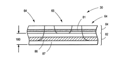
atoms)がボロンをドープした層または領域86に達することを効果的に制限し、それによって、侵入物トラップ材料81が無くても狭いベース幅180を維持することができる。バイポーラトランジスタのベースは、デバイスの電流スイッチング能力を制御する領域である。ベースを通って注入された小数キャリアの走行時間は、ベース幅の2乗にほぼ比例するので、ベース幅の縮小によって、劇的にベース走行時間が減少するが、それは、単一電流利得fτの周波数とは逆比例の関係にある。従って、より狭いベースを有するバイポーラトランジスタは、より高い周波数で電流をスイッチングすることができる。
Claims (3)
- ヘテロ接合エピタキシャル・スタック(30)を具備する半導体基板(11)に形成されたNPNヘテロ接合バイポーラトランジスタ(100)において、
前記ヘテロ接合エピタキシャル・スタック(30)は、
前記トランジスタのベース領域を形成するためのヘテロ接合層(82)であって、前記ヘテロ接合層(82)は、侵入物トラップ材料の領域(87)を含む第1SiGe部、および、前記第1SiGe部に隣接して形成され、かつp型ドープ領域(86)を含む第2SiGe部を含み、前記第2SiGe部は、前記侵入物トラップ材料を含まないで形成される、ヘテロ接合層(82)と、
前記トランジスタのエミッタ領域を形成するために前記ヘテロ接合層(82)に隣接して形成されたキャップ層(84)であって、前記ヘテロ接合層(82)と前記キャップ層(84)との間の境界は、エミッタ−ベース接合を形成し、前記キャップ層(84)は、侵入物トラップ材料の層(81)を有するシリコン領域を含み、前記侵入物トラップ材料の層(81)および前記侵入物トラップ材料の領域(87)は分離され、かつ重なり合わず、前記侵入物トラップ材料の層(81)は、前記エミッタ−ベース接合から離間している、キャップ層(84)と、からなり、
前記侵入物トラップ材料は、炭素である、
ことを特徴とするNPNヘテロ接合バイポーラトランジスタ。 - NPNヘテロ接合バイポーラトランジスタ(100)を形成する方法において、
半導体基板(11)を提供する段階と、
前記半導体基板上に侵入物トラップ材料の領域(87)を含む第1SiGe部を形成する段階と、
前記第1SiGe部上にp型にドープされた領域を含む第2SiGe層(86)を形成する段階であって、前記第2SiGe層は侵入物トラップ材料を含まないで形成され、かつ前記第1および第2SiGe部は、前記NPNヘテロ接合バイポーラトランジスタのベース領域(82)を形成する、段階と、
前記第2SiGe部上にシリコン領域(84)を形成する段階であって、前記シリコン領域はn型ドーパントを含み、かつ前記第2SiGe部とエミッタ−ベース接合を形成し、また前記シリコン領域は侵入物トラップ材料の層(81)を含み、さらに前記侵入物トラップ材料の層はエミッタ−ベース接合から離間しており、かつ前記侵入物トラップ材料の領域(87)および前記侵入物トラップ材料の層(81)は重なり合わない、段階と、
前記シリコン領域上にシリコンを含む誘電層を形成する段階であって、前記侵入物トラップ材料の層は、前記誘電層を形成する間、前記ベース領域にシリコン侵入物の注入を抑制するために構成される、段階と、
から構成され、
前記侵入物トラップ材料は、炭素である、
ことを特徴とする方法。 - 前記ベース領域(82)は、前記シリコン領域(84)によって前記誘電層から分離されることを特徴とする請求項2記載の方法。
Applications Claiming Priority (2)
| Application Number | Priority Date | Filing Date | Title |
|---|---|---|---|
| US10/307590 | 2002-12-02 | ||
| US10/307,590 US6764918B2 (en) | 2002-12-02 | 2002-12-02 | Structure and method of making a high performance semiconductor device having a narrow doping profile |
Publications (2)
| Publication Number | Publication Date |
|---|---|
| JP2004186675A JP2004186675A (ja) | 2004-07-02 |
| JP4807931B2 true JP4807931B2 (ja) | 2011-11-02 |
Family
ID=32312201
Family Applications (1)
| Application Number | Title | Priority Date | Filing Date |
|---|---|---|---|
| JP2003373787A Expired - Fee Related JP4807931B2 (ja) | 2002-12-02 | 2003-10-31 | 狭いドーピング・プロファイルを有する高性能半導体デバイスを作成する構造および方法 |
Country Status (4)
| Country | Link |
|---|---|
| US (1) | US6764918B2 (ja) |
| JP (1) | JP4807931B2 (ja) |
| CN (1) | CN100463217C (ja) |
| DE (1) | DE10352765B4 (ja) |
Families Citing this family (15)
| Publication number | Priority date | Publication date | Assignee | Title |
|---|---|---|---|---|
| JP2007505505A (ja) * | 2004-01-10 | 2007-03-08 | エイチブイブイアイ・セミコンダクターズ・インコーポレイテッド | パワー半導体装置およびそのための方法 |
| US7923339B2 (en) * | 2004-12-06 | 2011-04-12 | Nxp B.V. | Method of producing an epitaxial layer on semiconductor substrate and device produced with such a method |
| US8530963B2 (en) * | 2005-01-06 | 2013-09-10 | Estivation Properties Llc | Power semiconductor device and method therefor |
| US7300849B2 (en) * | 2005-11-04 | 2007-11-27 | Atmel Corporation | Bandgap engineered mono-crystalline silicon cap layers for SiGe HBT performance enhancement |
| US7651919B2 (en) * | 2005-11-04 | 2010-01-26 | Atmel Corporation | Bandgap and recombination engineered emitter layers for SiGe HBT performance optimization |
| US20070102729A1 (en) * | 2005-11-04 | 2007-05-10 | Enicks Darwin G | Method and system for providing a heterojunction bipolar transistor having SiGe extensions |
| US7439558B2 (en) * | 2005-11-04 | 2008-10-21 | Atmel Corporation | Method and system for controlled oxygen incorporation in compound semiconductor films for device performance enhancement |
| US7656003B2 (en) * | 2006-08-25 | 2010-02-02 | Hvvi Semiconductors, Inc | Electrical stress protection apparatus and method of manufacture |
| US7888746B2 (en) * | 2006-12-15 | 2011-02-15 | Hvvi Semiconductors, Inc. | Semiconductor structure and method of manufacture |
| US8471307B2 (en) * | 2008-06-13 | 2013-06-25 | Texas Instruments Incorporated | In-situ carbon doped e-SiGeCB stack for MOS transistor |
| EP2202795A1 (en) * | 2008-12-24 | 2010-06-30 | S.O.I. TEC Silicon | Method for fabricating a semiconductor substrate and semiconductor substrate |
| EP2581930B1 (en) * | 2011-10-11 | 2014-06-04 | Nxp B.V. | Bipolar transistor manufacturing method, bipolar transistor and integrated circuit |
| US9466698B2 (en) * | 2013-03-15 | 2016-10-11 | Semiconductor Components Industries, Llc | Electronic device including vertical conductive regions and a process of forming the same |
| CN103325680A (zh) * | 2013-04-24 | 2013-09-25 | 苏州硅智源微电子有限公司 | 提高集成电路双极型三极管抗辐射的方法 |
| TWI743788B (zh) * | 2020-05-18 | 2021-10-21 | 力晶積成電子製造股份有限公司 | 電晶體及其製造方法 |
Family Cites Families (10)
| Publication number | Priority date | Publication date | Assignee | Title |
|---|---|---|---|---|
| JPH05293328A (ja) * | 1992-04-17 | 1993-11-09 | Nitto Denko Corp | 可燃性有機蒸気含有空気の処理方法 |
| US5365089A (en) * | 1992-12-23 | 1994-11-15 | International Business Machines Corporation | Double heterojunction bipolar transistor and the method of manufacture therefor |
| JP2611640B2 (ja) * | 1993-12-20 | 1997-05-21 | 日本電気株式会社 | ヘテロ接合バイポーラトランジスタ |
| JP3549408B2 (ja) * | 1998-09-03 | 2004-08-04 | 松下電器産業株式会社 | バイポーラトランジスタ |
| CN1111313C (zh) * | 1999-07-02 | 2003-06-11 | 北京工业大学 | 异质结双极型晶体管 |
| US6316795B1 (en) * | 2000-04-03 | 2001-11-13 | Hrl Laboratories, Llc | Silicon-carbon emitter for silicon-germanium heterojunction bipolar transistors |
| US6387768B1 (en) * | 2000-08-29 | 2002-05-14 | Semiconductor Components Industries Llc | Method of manufacturing a semiconductor component and semiconductor component thereof |
| US6362065B1 (en) * | 2001-02-26 | 2002-03-26 | Texas Instruments Incorporated | Blocking of boron diffusion through the emitter-emitter poly interface in PNP HBTs through use of a SiC layer at the top of the emitter epi layer |
| US6506659B2 (en) * | 2001-03-17 | 2003-01-14 | Newport Fab, Llc | High performance bipolar transistor |
| US7064416B2 (en) * | 2001-11-16 | 2006-06-20 | International Business Machines Corporation | Semiconductor device and method having multiple subcollectors formed on a common wafer |
-
2002
- 2002-12-02 US US10/307,590 patent/US6764918B2/en not_active Expired - Lifetime
-
2003
- 2003-10-31 JP JP2003373787A patent/JP4807931B2/ja not_active Expired - Fee Related
- 2003-11-12 DE DE10352765A patent/DE10352765B4/de not_active Expired - Fee Related
- 2003-11-28 CN CNB2003101186870A patent/CN100463217C/zh not_active Expired - Fee Related
Also Published As
| Publication number | Publication date |
|---|---|
| US6764918B2 (en) | 2004-07-20 |
| US20040106264A1 (en) | 2004-06-03 |
| DE10352765A1 (de) | 2004-06-09 |
| CN100463217C (zh) | 2009-02-18 |
| HK1065644A1 (zh) | 2005-02-25 |
| JP2004186675A (ja) | 2004-07-02 |
| DE10352765B4 (de) | 2013-03-28 |
| CN1505168A (zh) | 2004-06-16 |
Similar Documents
| Publication | Publication Date | Title |
|---|---|---|
| US5428243A (en) | Bipolar transistor with a self-aligned heavily doped collector region and base link regions. | |
| JP4807931B2 (ja) | 狭いドーピング・プロファイルを有する高性能半導体デバイスを作成する構造および方法 | |
| US9871125B2 (en) | Bipolar transistor | |
| JPH06101470B2 (ja) | スロット内に形成されたバイポーラトランジスタからなる能動要素を有する集積回路装置 | |
| JP2011238955A (ja) | バイポーラトランジスタ | |
| JP2005509273A5 (ja) | ||
| US6858485B2 (en) | Method for creation of a very narrow emitter feature | |
| US5484737A (en) | Method for fabricating bipolar transistor | |
| US8872237B2 (en) | Heterojunction bipolar transistor manufacturing method and integrated circuit comprising a heterojunction bipolar transistor | |
| US6180442B1 (en) | Bipolar transistor with an inhomogeneous emitter in a BICMOS integrated circuit method | |
| KR100455829B1 (ko) | 초자기정렬 이종접합 바이폴라 소자 및 그 제조방법 | |
| JPH04102335A (ja) | セルフアライン接触を有するバイポーラトランジスタの製作プロセス | |
| JP2001319936A (ja) | バイポーラトランジスタ及びその製造方法 | |
| JP2515055B2 (ja) | 半導体デバイス | |
| JP2008235560A (ja) | ヘテロ接合バイポーラトランジスタ | |
| KR101118649B1 (ko) | 바이폴라 트랜지스터 및 그 형성 방법 | |
| JP2001196382A (ja) | 半導体装置及びその製造方法 | |
| US7235861B1 (en) | NPN transistor having reduced extrinsic base resistance and improved manufacturability | |
| US6387768B1 (en) | Method of manufacturing a semiconductor component and semiconductor component thereof | |
| JP3278493B2 (ja) | 半導体装置およびその製造方法 | |
| JPS6241427B2 (ja) | ||
| HK1065644B (en) | Structure and method of making a high performance semiconductor device having a narrow doping profile | |
| JPH05109748A (ja) | 半導体装置およびその製造方法 | |
| JP2827696B2 (ja) | 半導体装置の製造方法 | |
| JP2008544562A (ja) | 半導体デバイス及びその製造方法 |
Legal Events
| Date | Code | Title | Description |
|---|---|---|---|
| A621 | Written request for application examination |
Free format text: JAPANESE INTERMEDIATE CODE: A621 Effective date: 20060815 |
|
| A977 | Report on retrieval |
Free format text: JAPANESE INTERMEDIATE CODE: A971007 Effective date: 20100608 |
|
| A131 | Notification of reasons for refusal |
Free format text: JAPANESE INTERMEDIATE CODE: A131 Effective date: 20100803 |
|
| A521 | Request for written amendment filed |
Free format text: JAPANESE INTERMEDIATE CODE: A523 Effective date: 20101005 |
|
| A131 | Notification of reasons for refusal |
Free format text: JAPANESE INTERMEDIATE CODE: A131 Effective date: 20110418 |
|
| A521 | Request for written amendment filed |
Free format text: JAPANESE INTERMEDIATE CODE: A523 Effective date: 20110719 |
|
| TRDD | Decision of grant or rejection written | ||
| A01 | Written decision to grant a patent or to grant a registration (utility model) |
Free format text: JAPANESE INTERMEDIATE CODE: A01 Effective date: 20110815 |
|
| A01 | Written decision to grant a patent or to grant a registration (utility model) |
Free format text: JAPANESE INTERMEDIATE CODE: A01 |
|
| A61 | First payment of annual fees (during grant procedure) |
Free format text: JAPANESE INTERMEDIATE CODE: A61 Effective date: 20110816 |
|
| FPAY | Renewal fee payment (event date is renewal date of database) |
Free format text: PAYMENT UNTIL: 20140826 Year of fee payment: 3 |
|
| R150 | Certificate of patent or registration of utility model |
Ref document number: 4807931 Country of ref document: JP Free format text: JAPANESE INTERMEDIATE CODE: R150 |
|
| R250 | Receipt of annual fees |
Free format text: JAPANESE INTERMEDIATE CODE: R250 |
|
| R250 | Receipt of annual fees |
Free format text: JAPANESE INTERMEDIATE CODE: R250 |
|
| R250 | Receipt of annual fees |
Free format text: JAPANESE INTERMEDIATE CODE: R250 |
|
| R250 | Receipt of annual fees |
Free format text: JAPANESE INTERMEDIATE CODE: R250 |
|
| R250 | Receipt of annual fees |
Free format text: JAPANESE INTERMEDIATE CODE: R250 |
|
| R250 | Receipt of annual fees |
Free format text: JAPANESE INTERMEDIATE CODE: R250 |
|
| R250 | Receipt of annual fees |
Free format text: JAPANESE INTERMEDIATE CODE: R250 |
|
| R250 | Receipt of annual fees |
Free format text: JAPANESE INTERMEDIATE CODE: R250 |
|
| R250 | Receipt of annual fees |
Free format text: JAPANESE INTERMEDIATE CODE: R250 |
|
| LAPS | Cancellation because of no payment of annual fees |