JP4817827B2 - 半導体装置 - Google Patents
半導体装置 Download PDFInfo
- Publication number
- JP4817827B2 JP4817827B2 JP2005356109A JP2005356109A JP4817827B2 JP 4817827 B2 JP4817827 B2 JP 4817827B2 JP 2005356109 A JP2005356109 A JP 2005356109A JP 2005356109 A JP2005356109 A JP 2005356109A JP 4817827 B2 JP4817827 B2 JP 4817827B2
- Authority
- JP
- Japan
- Prior art keywords
- trench
- semiconductor device
- electrode
- insulating film
- type
- Prior art date
- Legal status (The legal status is an assumption and is not a legal conclusion. Google has not performed a legal analysis and makes no representation as to the accuracy of the status listed.)
- Expired - Fee Related
Links
Images




Classifications
-
- H—ELECTRICITY
- H10—SEMICONDUCTOR DEVICES; ELECTRIC SOLID-STATE DEVICES NOT OTHERWISE PROVIDED FOR
- H10D—INORGANIC ELECTRIC SEMICONDUCTOR DEVICES
- H10D30/00—Field-effect transistors [FET]
- H10D30/60—Insulated-gate field-effect transistors [IGFET]
- H10D30/64—Double-diffused metal-oxide semiconductor [DMOS] FETs
- H10D30/66—Vertical DMOS [VDMOS] FETs
- H10D30/668—Vertical DMOS [VDMOS] FETs having trench gate electrodes, e.g. UMOS transistors
-
- H—ELECTRICITY
- H10—SEMICONDUCTOR DEVICES; ELECTRIC SOLID-STATE DEVICES NOT OTHERWISE PROVIDED FOR
- H10D—INORGANIC ELECTRIC SEMICONDUCTOR DEVICES
- H10D12/00—Bipolar devices controlled by the field effect, e.g. insulated-gate bipolar transistors [IGBT]
- H10D12/411—Insulated-gate bipolar transistors [IGBT]
- H10D12/441—Vertical IGBTs
- H10D12/461—Vertical IGBTs having non-planar surfaces, e.g. having trenches, recesses or pillars in the surfaces of the emitter, base or collector regions
- H10D12/481—Vertical IGBTs having non-planar surfaces, e.g. having trenches, recesses or pillars in the surfaces of the emitter, base or collector regions having gate structures on slanted surfaces, on vertical surfaces, or in grooves, e.g. trench gate IGBTs
-
- H—ELECTRICITY
- H10—SEMICONDUCTOR DEVICES; ELECTRIC SOLID-STATE DEVICES NOT OTHERWISE PROVIDED FOR
- H10D—INORGANIC ELECTRIC SEMICONDUCTOR DEVICES
- H10D30/00—Field-effect transistors [FET]
- H10D30/01—Manufacture or treatment
- H10D30/021—Manufacture or treatment of FETs having insulated gates [IGFET]
- H10D30/028—Manufacture or treatment of FETs having insulated gates [IGFET] of double-diffused metal oxide semiconductor [DMOS] FETs
- H10D30/0291—Manufacture or treatment of FETs having insulated gates [IGFET] of double-diffused metal oxide semiconductor [DMOS] FETs of vertical DMOS [VDMOS] FETs
- H10D30/0293—Manufacture or treatment of FETs having insulated gates [IGFET] of double-diffused metal oxide semiconductor [DMOS] FETs of vertical DMOS [VDMOS] FETs using formation of insulating sidewall spacers
-
- H—ELECTRICITY
- H10—SEMICONDUCTOR DEVICES; ELECTRIC SOLID-STATE DEVICES NOT OTHERWISE PROVIDED FOR
- H10D—INORGANIC ELECTRIC SEMICONDUCTOR DEVICES
- H10D30/00—Field-effect transistors [FET]
- H10D30/01—Manufacture or treatment
- H10D30/021—Manufacture or treatment of FETs having insulated gates [IGFET]
- H10D30/028—Manufacture or treatment of FETs having insulated gates [IGFET] of double-diffused metal oxide semiconductor [DMOS] FETs
- H10D30/0291—Manufacture or treatment of FETs having insulated gates [IGFET] of double-diffused metal oxide semiconductor [DMOS] FETs of vertical DMOS [VDMOS] FETs
- H10D30/0297—Manufacture or treatment of FETs having insulated gates [IGFET] of double-diffused metal oxide semiconductor [DMOS] FETs of vertical DMOS [VDMOS] FETs using recessing of the gate electrodes, e.g. to form trench gate electrodes
-
- H—ELECTRICITY
- H10—SEMICONDUCTOR DEVICES; ELECTRIC SOLID-STATE DEVICES NOT OTHERWISE PROVIDED FOR
- H10D—INORGANIC ELECTRIC SEMICONDUCTOR DEVICES
- H10D64/00—Electrodes of devices having potential barriers
- H10D64/111—Field plates
- H10D64/117—Recessed field plates, e.g. trench field plates or buried field plates
-
- H—ELECTRICITY
- H10—SEMICONDUCTOR DEVICES; ELECTRIC SOLID-STATE DEVICES NOT OTHERWISE PROVIDED FOR
- H10D—INORGANIC ELECTRIC SEMICONDUCTOR DEVICES
- H10D64/00—Electrodes of devices having potential barriers
- H10D64/20—Electrodes characterised by their shapes, relative sizes or dispositions
- H10D64/27—Electrodes not carrying the current to be rectified, amplified, oscillated or switched, e.g. gates
- H10D64/311—Gate electrodes for field-effect devices
- H10D64/411—Gate electrodes for field-effect devices for FETs
- H10D64/511—Gate electrodes for field-effect devices for FETs for IGFETs
- H10D64/512—Disposition of the gate electrodes, e.g. buried gates
- H10D64/513—Disposition of the gate electrodes, e.g. buried gates within recesses in the substrate, e.g. trench gates, groove gates or buried gates
-
- H—ELECTRICITY
- H10—SEMICONDUCTOR DEVICES; ELECTRIC SOLID-STATE DEVICES NOT OTHERWISE PROVIDED FOR
- H10D—INORGANIC ELECTRIC SEMICONDUCTOR DEVICES
- H10D62/00—Semiconductor bodies, or regions thereof, of devices having potential barriers
- H10D62/10—Shapes, relative sizes or dispositions of the regions of the semiconductor bodies; Shapes of the semiconductor bodies
- H10D62/13—Semiconductor regions connected to electrodes carrying current to be rectified, amplified or switched, e.g. source or drain regions
- H10D62/149—Source or drain regions of field-effect devices
- H10D62/151—Source or drain regions of field-effect devices of IGFETs
- H10D62/156—Drain regions of DMOS transistors
- H10D62/157—Impurity concentrations or distributions
-
- H—ELECTRICITY
- H10—SEMICONDUCTOR DEVICES; ELECTRIC SOLID-STATE DEVICES NOT OTHERWISE PROVIDED FOR
- H10D—INORGANIC ELECTRIC SEMICONDUCTOR DEVICES
- H10D64/00—Electrodes of devices having potential barriers
- H10D64/01—Manufacture or treatment
- H10D64/013—Manufacture or treatment of electrodes having a conductor capacitively coupled to a semiconductor by an insulator
- H10D64/01302—Manufacture or treatment of electrodes having a conductor capacitively coupled to a semiconductor by an insulator the insulator being formed after the semiconductor body, the semiconductor being silicon
- H10D64/01304—Manufacture or treatment of electrodes having a conductor capacitively coupled to a semiconductor by an insulator the insulator being formed after the semiconductor body, the semiconductor being silicon characterised by the conductor
- H10D64/01326—Aspects related to lithography, isolation or planarisation of the conductor
- H10D64/0133—Aspects related to lithography, isolation or planarisation of the conductor at least part of the entire electrode being a sidewall spacer, being formed by transformation under a mask or being formed by plating at a sidewall
-
- H—ELECTRICITY
- H10—SEMICONDUCTOR DEVICES; ELECTRIC SOLID-STATE DEVICES NOT OTHERWISE PROVIDED FOR
- H10D—INORGANIC ELECTRIC SEMICONDUCTOR DEVICES
- H10D64/00—Electrodes of devices having potential barriers
- H10D64/20—Electrodes characterised by their shapes, relative sizes or dispositions
- H10D64/27—Electrodes not carrying the current to be rectified, amplified, oscillated or switched, e.g. gates
- H10D64/311—Gate electrodes for field-effect devices
- H10D64/411—Gate electrodes for field-effect devices for FETs
- H10D64/511—Gate electrodes for field-effect devices for FETs for IGFETs
- H10D64/514—Gate electrodes for field-effect devices for FETs for IGFETs characterised by the insulating layers
- H10D64/516—Gate electrodes for field-effect devices for FETs for IGFETs characterised by the insulating layers the thicknesses being non-uniform
-
- H—ELECTRICITY
- H10—SEMICONDUCTOR DEVICES; ELECTRIC SOLID-STATE DEVICES NOT OTHERWISE PROVIDED FOR
- H10D—INORGANIC ELECTRIC SEMICONDUCTOR DEVICES
- H10D64/00—Electrodes of devices having potential barriers
- H10D64/20—Electrodes characterised by their shapes, relative sizes or dispositions
- H10D64/27—Electrodes not carrying the current to be rectified, amplified, oscillated or switched, e.g. gates
- H10D64/311—Gate electrodes for field-effect devices
- H10D64/411—Gate electrodes for field-effect devices for FETs
- H10D64/511—Gate electrodes for field-effect devices for FETs for IGFETs
- H10D64/517—Gate electrodes for field-effect devices for FETs for IGFETs characterised by the conducting layers
- H10D64/518—Gate electrodes for field-effect devices for FETs for IGFETs characterised by the conducting layers characterised by their lengths or sectional shapes
Landscapes
- Electrodes Of Semiconductors (AREA)
Description
Claims (4)
- 第1導電型の半導体領域と、
前記半導体領域に接続される第1主電極と、
前記半導体領域上に形成された第2導電型のベース領域と、
前記ベース領域上に形成された第1導電型の拡散領域と、
該拡散領域と前記ベース領域に接続される第2主電極と、
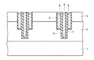
前記拡散領域上面から前記半導体領域に達するように形成された第1トレンチと、
該第1トレンチから前記第1トレンチよりさらに深く形成された第2トレンチと、
前記第1トレンチの側面に第1絶縁膜を介して形成されたゲート電極と、
前記第2トレンチに第2絶縁膜を介して前記ゲート電極より下方に突出して形成されるとともに前記第2主電極または前記ゲート電極のいずれか一方と接続された突出電極とを備え、
前記ゲート電極と前記突出電極は、前記第1トレンチの深さ方向に直交する方向に第3絶縁膜を介して並ぶように配置され、
前記ゲート電極は、少なくとも一対設けられ、
一対の前記ゲート電極は、1つの前記突出電極を前記第3絶縁膜を介して挟むように配置されている
ことを特徴とする半導体装置。 - 前記第2絶縁膜は、前記第1絶縁膜と比較して厚く形成されていることを特徴とする請求項1記載の半導体装置。
- 前記突出電極は、前記ゲート電極が形成された深さ領域よりも深い位置にのみ形成されていることを特徴とする請求項1又は請求項2記載の半導体装置。
- 前記第2トレンチに隣接する前記半導体領域に前記半導体領域よりも不純物濃度が高い第1導電型の抵抗低減層が形成されていることを特徴とする請求項1乃至請求項3のいずれか1項記載の半導体装置。
Priority Applications (2)
| Application Number | Priority Date | Filing Date | Title |
|---|---|---|---|
| JP2005356109A JP4817827B2 (ja) | 2005-12-09 | 2005-12-09 | 半導体装置 |
| US11/608,538 US7719053B2 (en) | 2005-12-09 | 2006-12-08 | Semiconductor device having increased gate-source capacity provided by protruding electrode disposed between gate electrodes formed in a trench |
Applications Claiming Priority (1)
| Application Number | Priority Date | Filing Date | Title |
|---|---|---|---|
| JP2005356109A JP4817827B2 (ja) | 2005-12-09 | 2005-12-09 | 半導体装置 |
Publications (2)
| Publication Number | Publication Date |
|---|---|
| JP2007165380A JP2007165380A (ja) | 2007-06-28 |
| JP4817827B2 true JP4817827B2 (ja) | 2011-11-16 |
Family
ID=38172465
Family Applications (1)
| Application Number | Title | Priority Date | Filing Date |
|---|---|---|---|
| JP2005356109A Expired - Fee Related JP4817827B2 (ja) | 2005-12-09 | 2005-12-09 | 半導体装置 |
Country Status (2)
| Country | Link |
|---|---|
| US (1) | US7719053B2 (ja) |
| JP (1) | JP4817827B2 (ja) |
Families Citing this family (70)
| Publication number | Priority date | Publication date | Assignee | Title |
|---|---|---|---|---|
| US8093621B2 (en) | 2008-12-23 | 2012-01-10 | Power Integrations, Inc. | VTS insulated gate bipolar transistor |
| US8101995B2 (en) * | 2007-02-08 | 2012-01-24 | International Rectifier Corporation | Integrated MOSFET and Schottky device |
| JP2009164558A (ja) * | 2007-12-10 | 2009-07-23 | Toyota Central R&D Labs Inc | 半導体装置とその製造方法、並びにトレンチゲートの製造方法 |
| US7998808B2 (en) * | 2008-03-21 | 2011-08-16 | International Rectifier Corporation | Semiconductor device fabrication using spacers |
| JP2009259968A (ja) * | 2008-04-15 | 2009-11-05 | Nec Electronics Corp | 半導体装置及びその製造方法 |
| US7964912B2 (en) | 2008-09-18 | 2011-06-21 | Power Integrations, Inc. | High-voltage vertical transistor with a varied width silicon pillar |
| TW201015718A (en) * | 2008-10-03 | 2010-04-16 | Sanyo Electric Co | Semiconductor device and method for manufacturing the same |
| US20100155831A1 (en) * | 2008-12-20 | 2010-06-24 | Power Integrations, Inc. | Deep trench insulated gate bipolar transistor |
| US7871882B2 (en) | 2008-12-20 | 2011-01-18 | Power Integrations, Inc. | Method of fabricating a deep trench insulated gate bipolar transistor |
| US20110084332A1 (en) * | 2009-10-08 | 2011-04-14 | Vishay General Semiconductor, Llc. | Trench termination structure |
| CN102714217B (zh) * | 2010-01-04 | 2015-07-08 | 株式会社日立制作所 | 半导体装置及使用半导体装置的电力转换装置 |
| JP2012064641A (ja) * | 2010-09-14 | 2012-03-29 | Toshiba Corp | 半導体装置 |
| JP5631752B2 (ja) * | 2011-01-12 | 2014-11-26 | 株式会社 日立パワーデバイス | 半導体装置および電力変換装置 |
| JP5627494B2 (ja) * | 2011-02-09 | 2014-11-19 | 株式会社東芝 | 半導体装置およびその製造方法 |
| JP2012204590A (ja) * | 2011-03-25 | 2012-10-22 | Toshiba Corp | 半導体装置およびその製造方法 |
| JP5806535B2 (ja) * | 2011-07-20 | 2015-11-10 | 株式会社 日立パワーデバイス | 半導体装置及びそれを用いた電力変換装置 |
| CN102437191B (zh) * | 2011-12-06 | 2014-01-15 | 苏州硅能半导体科技股份有限公司 | 低栅漏电容的沟槽mos器件及其制造方法 |
| KR101250649B1 (ko) * | 2011-12-26 | 2013-04-03 | 삼성전기주식회사 | 반도체 소자 및 이의 제조 방법 |
| US8653600B2 (en) | 2012-06-01 | 2014-02-18 | Power Integrations, Inc. | High-voltage monolithic schottky device structure |
| US9293376B2 (en) | 2012-07-11 | 2016-03-22 | Taiwan Semiconductor Manufacturing Company, Ltd. | Apparatus and method for power MOS transistor |
| US8765609B2 (en) * | 2012-07-25 | 2014-07-01 | Power Integrations, Inc. | Deposit/etch for tapered oxide |
| JP5802636B2 (ja) | 2012-09-18 | 2015-10-28 | 株式会社東芝 | 半導体装置およびその製造方法 |
| JP2014063931A (ja) * | 2012-09-21 | 2014-04-10 | Toshiba Corp | 電力用半導体素子 |
| JP2014067753A (ja) * | 2012-09-24 | 2014-04-17 | Toshiba Corp | 電力用半導体素子 |
| JP5867617B2 (ja) * | 2012-10-17 | 2016-02-24 | 富士電機株式会社 | 半導体装置 |
| US20140167152A1 (en) * | 2012-12-13 | 2014-06-19 | International Rectifier Corporation | Reduced Gate Charge Trench Field-Effect Transistor |
| US9391191B2 (en) * | 2012-12-13 | 2016-07-12 | Infineon Technologies Americas Corp. | Trench FET having merged gate dielectric |
| JP2014120656A (ja) * | 2012-12-18 | 2014-06-30 | Toshiba Corp | 半導体装置 |
| JP5799046B2 (ja) * | 2013-03-22 | 2015-10-21 | 株式会社東芝 | 半導体装置 |
| JP5875026B2 (ja) * | 2013-09-20 | 2016-03-02 | サンケン電気株式会社 | 半導体装置 |
| JP2016040820A (ja) * | 2013-09-20 | 2016-03-24 | サンケン電気株式会社 | 半導体装置 |
| CN104465718B (zh) * | 2013-09-20 | 2017-07-14 | 三垦电气株式会社 | 半导体装置 |
| JP6173987B2 (ja) | 2013-09-20 | 2017-08-02 | サンケン電気株式会社 | 半導体装置 |
| KR101701240B1 (ko) * | 2013-09-20 | 2017-02-01 | 산켄덴키 가부시키가이샤 | 반도체 장치 |
| US9543396B2 (en) | 2013-12-13 | 2017-01-10 | Power Integrations, Inc. | Vertical transistor device structure with cylindrically-shaped regions |
| US10325988B2 (en) | 2013-12-13 | 2019-06-18 | Power Integrations, Inc. | Vertical transistor device structure with cylindrically-shaped field plates |
| JP2016167519A (ja) * | 2015-03-09 | 2016-09-15 | 株式会社東芝 | 半導体装置 |
| JP6310577B2 (ja) * | 2015-04-17 | 2018-04-11 | スー ジョウ オリエンタル セミコンダクター カンパニー リミテッドSu Zhou Oriental Semiconductor Co., Ltd. | スプリットゲート型パワーデバイスの製造方法 |
| US9391194B1 (en) * | 2015-06-19 | 2016-07-12 | Sanken Electric Co., Ltd. | High voltage vertical FPMOS fets |
| CN106549056B (zh) * | 2015-09-22 | 2019-07-30 | 大中积体电路股份有限公司 | 双栅极沟槽式功率晶体管及其制造方法 |
| JP2017126635A (ja) * | 2016-01-13 | 2017-07-20 | サンケン電気株式会社 | 半導体装置 |
| US10128368B2 (en) * | 2016-01-13 | 2018-11-13 | Sinopower Semiconductor, Inc. | Double gate trench power transistor and manufacturing method thereof |
| CN105789288B (zh) * | 2016-03-15 | 2019-05-03 | 江苏中科君芯科技有限公司 | 具有集成栅源电容的igbt器件 |
| CN108886054B (zh) * | 2016-03-31 | 2021-05-25 | 新电元工业株式会社 | 半导体装置的制造方法以及半导体装置 |
| JP6519894B2 (ja) * | 2016-03-31 | 2019-05-29 | 新電元工業株式会社 | 半導体装置の製造方法及び半導体装置 |
| CN105870022B (zh) * | 2016-05-31 | 2019-01-04 | 上海华虹宏力半导体制造有限公司 | 屏蔽栅沟槽mosfet的制造方法 |
| US10622435B2 (en) * | 2016-07-29 | 2020-04-14 | Sony Corporation | Display device, manufacturing method of display device, and electronic device |
| CN108346692B (zh) * | 2017-01-25 | 2023-11-21 | 杭州士兰集成电路有限公司 | 功率半导体器件及其制造方法 |
| US10361298B2 (en) * | 2017-11-27 | 2019-07-23 | Sanken Electric Co., Ltd. | Semiconductor device having improved trench and electrode structures |
| KR102246501B1 (ko) * | 2017-12-29 | 2021-04-30 | 수 조우 오리엔탈 세미컨덕터 콤퍼니 리미티드 | 반도체 전력 소자 |
| CN110137249A (zh) * | 2018-02-09 | 2019-08-16 | 苏州东微半导体有限公司 | Igbt功率器件及其制造方法 |
| JP7118914B2 (ja) * | 2019-03-15 | 2022-08-16 | 株式会社東芝 | 半導体装置及びその製造方法 |
| TW202038470A (zh) | 2019-04-10 | 2020-10-16 | 台灣茂矽電子股份有限公司 | 金氧半場效電晶體及其製造方法 |
| CN111933527A (zh) * | 2019-05-13 | 2020-11-13 | 上海先进半导体制造股份有限公司 | 沟槽igbt和其制作方法 |
| CN112864019A (zh) * | 2019-11-28 | 2021-05-28 | 苏州东微半导体股份有限公司 | 半导体功率器件的制造方法及半导体功率器件 |
| CN113394277B (zh) * | 2020-03-11 | 2022-05-20 | 珠海格力电器股份有限公司 | 沟槽栅igbt的元胞结构、其制备方法及沟槽栅igbt |
| JP7256770B2 (ja) * | 2020-03-16 | 2023-04-12 | 株式会社東芝 | 半導体装置 |
| CN111883583A (zh) * | 2020-07-31 | 2020-11-03 | 上海华虹宏力半导体制造有限公司 | 屏蔽栅沟槽功率器件及其制造方法 |
| CN112164648A (zh) * | 2020-09-29 | 2021-01-01 | 上海华虹宏力半导体制造有限公司 | 半导体器件的制备方法 |
| CN112271134B (zh) * | 2020-10-20 | 2021-10-22 | 苏州东微半导体股份有限公司 | 半导体功率器件的制造方法 |
| US11444164B2 (en) * | 2020-11-09 | 2022-09-13 | Nami MOS CO., LTD. | Shielded gate trench MOSFET having improved specific on-resistance structures |
| US11444167B2 (en) * | 2020-11-18 | 2022-09-13 | Advanced Power Electronics Corp. | Method of manufacturing trench type semiconductor device |
| JP7482083B2 (ja) * | 2021-06-02 | 2024-05-13 | 株式会社東芝 | 半導体装置及びその製造方法 |
| JP7472090B2 (ja) * | 2021-09-15 | 2024-04-22 | 株式会社東芝 | 半導体装置及び半導体装置の製造方法 |
| CN114975099B (zh) * | 2022-01-06 | 2025-08-19 | 上海华虹宏力半导体制造有限公司 | 一种屏蔽栅mosfet器件及其制作方法 |
| US20240297240A1 (en) * | 2023-03-01 | 2024-09-05 | Stmicroelectronics International N.V. | Split-gate trench power mosfet with thick poly-to-poly isolation |
| CN119230399B (zh) * | 2024-09-29 | 2025-03-11 | 苏州东微半导体股份有限公司 | 一种igbt器件的制造方法 |
| CN119230398B (zh) * | 2024-09-29 | 2025-05-23 | 苏州东微半导体股份有限公司 | Igbt器件的制造方法 |
| CN119230400B (zh) * | 2024-09-29 | 2025-10-17 | 苏州东微半导体股份有限公司 | Igbt器件的制造方法 |
| CN120786933B (zh) * | 2025-09-08 | 2025-12-12 | 广东芯粤能半导体有限公司 | 功率器件及其制备方法、电子设备 |
Family Cites Families (15)
| Publication number | Priority date | Publication date | Assignee | Title |
|---|---|---|---|---|
| US4893160A (en) * | 1987-11-13 | 1990-01-09 | Siliconix Incorporated | Method for increasing the performance of trenched devices and the resulting structure |
| JP2753155B2 (ja) * | 1990-06-13 | 1998-05-18 | 株式会社東芝 | 縦型mosトランジスタとその製造方法 |
| JP3198200B2 (ja) * | 1993-04-30 | 2001-08-13 | 株式会社東芝 | 縦型mosトランジスタの製造方法 |
| US5998833A (en) * | 1998-10-26 | 1999-12-07 | North Carolina State University | Power semiconductor devices having improved high frequency switching and breakdown characteristics |
| EP1166363B1 (en) * | 1999-03-01 | 2011-06-29 | GENERAL SEMICONDUCTOR, Inc. | Trench dmos transistor structure having a low resistance path to a drain contact located on an upper surface |
| JP4924781B2 (ja) * | 1999-10-13 | 2012-04-25 | 株式会社豊田中央研究所 | 縦型半導体装置 |
| JP4528460B2 (ja) * | 2000-06-30 | 2010-08-18 | 株式会社東芝 | 半導体素子 |
| JP4150496B2 (ja) * | 2000-12-28 | 2008-09-17 | 株式会社日立製作所 | 半導体装置及びその製造方法 |
| US6870220B2 (en) * | 2002-08-23 | 2005-03-22 | Fairchild Semiconductor Corporation | Method and apparatus for improved MOS gating to reduce miller capacitance and switching losses |
| US7345342B2 (en) * | 2001-01-30 | 2008-03-18 | Fairchild Semiconductor Corporation | Power semiconductor devices and methods of manufacture |
| DE10211543B4 (de) * | 2002-03-15 | 2005-06-30 | Infineon Technologies Ag | Schaltungsanordnung mit einem Feldeffekttransistor und Verfahren zum Betrieb der Schaltungsanordnung |
| CN100437942C (zh) * | 2002-05-31 | 2008-11-26 | Nxp股份有限公司 | 沟槽栅半导体器件及制造方法 |
| JP4202149B2 (ja) * | 2003-01-28 | 2008-12-24 | ローム株式会社 | 半導体装置およびその製造方法 |
| JP3742400B2 (ja) * | 2003-04-23 | 2006-02-01 | 株式会社東芝 | 半導体装置及びその製造方法 |
| GB0327791D0 (en) * | 2003-11-29 | 2003-12-31 | Koninkl Philips Electronics Nv | Trench insulated gate field effect transistor |
-
2005
- 2005-12-09 JP JP2005356109A patent/JP4817827B2/ja not_active Expired - Fee Related
-
2006
- 2006-12-08 US US11/608,538 patent/US7719053B2/en active Active
Also Published As
| Publication number | Publication date |
|---|---|
| JP2007165380A (ja) | 2007-06-28 |
| US20070138547A1 (en) | 2007-06-21 |
| US7719053B2 (en) | 2010-05-18 |
Similar Documents
| Publication | Publication Date | Title |
|---|---|---|
| JP4817827B2 (ja) | 半導体装置 | |
| CN111463277B (zh) | 半导体器件 | |
| US6930352B2 (en) | Insulated gate semiconductor device | |
| US7485921B2 (en) | Trench gate type MOS transistor semiconductor device | |
| US9515067B2 (en) | Semiconductor device having switching element and free wheel diode and method for controlling the same | |
| TWI509798B (zh) | 用於形成具多通道之屏蔽閘極溝槽場效電晶體(fet)的結構及方法 | |
| US6849880B1 (en) | Power semiconductor device | |
| TWI518911B (zh) | 垂直dmos電晶體 | |
| CN101454882B (zh) | 具有集成肖特基二极管的高密度沟槽fet及制造方法 | |
| EP1525621B1 (en) | Method of operating a trench gate semiconductor device | |
| US8154073B2 (en) | Semiconductor device | |
| JP4832731B2 (ja) | 電力用半導体装置 | |
| US8319289B2 (en) | Power MISFET, semiconductor device and DC/DC converter | |
| CN110176454B (zh) | 多晶体管器件 | |
| US6700156B2 (en) | Insulated gate semiconductor device | |
| JP5229288B2 (ja) | 半導体装置およびその制御方法 | |
| US8664716B2 (en) | Semiconductor device, method of manufacturing the same and power-supply device using the same | |
| JP2009033036A (ja) | 半導体装置及びこれを用いた電気回路装置 | |
| JP7158317B2 (ja) | 半導体装置 | |
| JPH08181313A (ja) | 横型トレンチmisfetおよびその製造方法 | |
| JP2004022693A (ja) | 半導体装置 | |
| US20140015044A1 (en) | Semiconductor device and method for manufacturing same | |
| JP2011517511A (ja) | 第1絶縁ゲート電界効果トランジスタが第2電界効果トランジスタと直列に接続された半導体デバイス | |
| JP5056147B2 (ja) | 半導体装置 | |
| KR20080014855A (ko) | 반도체 디바이스 |
Legal Events
| Date | Code | Title | Description |
|---|---|---|---|
| A977 | Report on retrieval |
Free format text: JAPANESE INTERMEDIATE CODE: A971007 Effective date: 20110223 |
|
| A131 | Notification of reasons for refusal |
Free format text: JAPANESE INTERMEDIATE CODE: A131 Effective date: 20110301 |
|
| A521 | Request for written amendment filed |
Free format text: JAPANESE INTERMEDIATE CODE: A523 Effective date: 20110428 |
|
| A131 | Notification of reasons for refusal |
Free format text: JAPANESE INTERMEDIATE CODE: A131 Effective date: 20110524 |
|
| A521 | Request for written amendment filed |
Free format text: JAPANESE INTERMEDIATE CODE: A523 Effective date: 20110715 |
|
| TRDD | Decision of grant or rejection written | ||
| A01 | Written decision to grant a patent or to grant a registration (utility model) |
Free format text: JAPANESE INTERMEDIATE CODE: A01 Effective date: 20110802 |
|
| A01 | Written decision to grant a patent or to grant a registration (utility model) |
Free format text: JAPANESE INTERMEDIATE CODE: A01 |
|
| A61 | First payment of annual fees (during grant procedure) |
Free format text: JAPANESE INTERMEDIATE CODE: A61 Effective date: 20110830 |
|
| FPAY | Renewal fee payment (event date is renewal date of database) |
Free format text: PAYMENT UNTIL: 20140909 Year of fee payment: 3 |
|
| R151 | Written notification of patent or utility model registration |
Ref document number: 4817827 Country of ref document: JP Free format text: JAPANESE INTERMEDIATE CODE: R151 |
|
| FPAY | Renewal fee payment (event date is renewal date of database) |
Free format text: PAYMENT UNTIL: 20140909 Year of fee payment: 3 |
|
| LAPS | Cancellation because of no payment of annual fees |