JP4819033B2 - 多層回路基板の製造方法 - Google Patents
多層回路基板の製造方法 Download PDFInfo
- Publication number
- JP4819033B2 JP4819033B2 JP2007500386A JP2007500386A JP4819033B2 JP 4819033 B2 JP4819033 B2 JP 4819033B2 JP 2007500386 A JP2007500386 A JP 2007500386A JP 2007500386 A JP2007500386 A JP 2007500386A JP 4819033 B2 JP4819033 B2 JP 4819033B2
- Authority
- JP
- Japan
- Prior art keywords
- circuit board
- double
- prepreg
- multilayer circuit
- thickness
- Prior art date
- Legal status (The legal status is an assumption and is not a legal conclusion. Google has not performed a legal analysis and makes no representation as to the accuracy of the status listed.)
- Expired - Fee Related
Links
Images




Classifications
-
- H—ELECTRICITY
- H05—ELECTRIC TECHNIQUES NOT OTHERWISE PROVIDED FOR
- H05K—PRINTED CIRCUITS; CASINGS OR CONSTRUCTIONAL DETAILS OF ELECTRIC APPARATUS; MANUFACTURE OF ASSEMBLAGES OF ELECTRICAL COMPONENTS
- H05K1/00—Printed circuits
- H05K1/02—Details
- H05K1/0213—Electrical arrangements not otherwise provided for
- H05K1/0237—High frequency adaptations
- H05K1/024—Dielectric details, e.g. changing the dielectric material around a transmission line
-
- H—ELECTRICITY
- H05—ELECTRIC TECHNIQUES NOT OTHERWISE PROVIDED FOR
- H05K—PRINTED CIRCUITS; CASINGS OR CONSTRUCTIONAL DETAILS OF ELECTRIC APPARATUS; MANUFACTURE OF ASSEMBLAGES OF ELECTRICAL COMPONENTS
- H05K3/00—Apparatus or processes for manufacturing printed circuits
- H05K3/46—Manufacturing multilayer circuits
- H05K3/4611—Manufacturing multilayer circuits by laminating two or more circuit boards
- H05K3/4614—Manufacturing multilayer circuits by laminating two or more circuit boards the electrical connections between the circuit boards being made during lamination
-
- H—ELECTRICITY
- H05—ELECTRIC TECHNIQUES NOT OTHERWISE PROVIDED FOR
- H05K—PRINTED CIRCUITS; CASINGS OR CONSTRUCTIONAL DETAILS OF ELECTRIC APPARATUS; MANUFACTURE OF ASSEMBLAGES OF ELECTRICAL COMPONENTS
- H05K3/00—Apparatus or processes for manufacturing printed circuits
- H05K3/46—Manufacturing multilayer circuits
- H05K3/4611—Manufacturing multilayer circuits by laminating two or more circuit boards
- H05K3/4614—Manufacturing multilayer circuits by laminating two or more circuit boards the electrical connections between the circuit boards being made during lamination
- H05K3/462—Manufacturing multilayer circuits by laminating two or more circuit boards the electrical connections between the circuit boards being made during lamination characterized by laminating only or mainly similar double-sided circuit boards
-
- H—ELECTRICITY
- H05—ELECTRIC TECHNIQUES NOT OTHERWISE PROVIDED FOR
- H05K—PRINTED CIRCUITS; CASINGS OR CONSTRUCTIONAL DETAILS OF ELECTRIC APPARATUS; MANUFACTURE OF ASSEMBLAGES OF ELECTRICAL COMPONENTS
- H05K2201/00—Indexing scheme relating to printed circuits covered by H05K1/00
- H05K2201/01—Dielectrics
- H05K2201/0183—Dielectric layers
- H05K2201/0191—Dielectric layers wherein the thickness of the dielectric plays an important role
-
- H—ELECTRICITY
- H05—ELECTRIC TECHNIQUES NOT OTHERWISE PROVIDED FOR
- H05K—PRINTED CIRCUITS; CASINGS OR CONSTRUCTIONAL DETAILS OF ELECTRIC APPARATUS; MANUFACTURE OF ASSEMBLAGES OF ELECTRICAL COMPONENTS
- H05K2201/00—Indexing scheme relating to printed circuits covered by H05K1/00
- H05K2201/03—Conductive materials
- H05K2201/0332—Structure of the conductor
- H05K2201/0335—Layered conductors or foils
- H05K2201/0355—Metal foils
-
- H—ELECTRICITY
- H05—ELECTRIC TECHNIQUES NOT OTHERWISE PROVIDED FOR
- H05K—PRINTED CIRCUITS; CASINGS OR CONSTRUCTIONAL DETAILS OF ELECTRIC APPARATUS; MANUFACTURE OF ASSEMBLAGES OF ELECTRICAL COMPONENTS
- H05K2201/00—Indexing scheme relating to printed circuits covered by H05K1/00
- H05K2201/09—Shape and layout
- H05K2201/09209—Shape and layout details of conductors
- H05K2201/0929—Conductive planes
- H05K2201/09318—Core having one signal plane and one power plane
-
- H—ELECTRICITY
- H05—ELECTRIC TECHNIQUES NOT OTHERWISE PROVIDED FOR
- H05K—PRINTED CIRCUITS; CASINGS OR CONSTRUCTIONAL DETAILS OF ELECTRIC APPARATUS; MANUFACTURE OF ASSEMBLAGES OF ELECTRICAL COMPONENTS
- H05K2201/00—Indexing scheme relating to printed circuits covered by H05K1/00
- H05K2201/09—Shape and layout
- H05K2201/09209—Shape and layout details of conductors
- H05K2201/0929—Conductive planes
- H05K2201/09327—Special sequence of power, ground and signal layers in multilayer PCB
-
- H—ELECTRICITY
- H05—ELECTRIC TECHNIQUES NOT OTHERWISE PROVIDED FOR
- H05K—PRINTED CIRCUITS; CASINGS OR CONSTRUCTIONAL DETAILS OF ELECTRIC APPARATUS; MANUFACTURE OF ASSEMBLAGES OF ELECTRICAL COMPONENTS
- H05K2201/00—Indexing scheme relating to printed circuits covered by H05K1/00
- H05K2201/10—Details of components or other objects attached to or integrated in a printed circuit board
- H05K2201/10227—Other objects, e.g. metallic pieces
- H05K2201/10378—Interposers
-
- H—ELECTRICITY
- H05—ELECTRIC TECHNIQUES NOT OTHERWISE PROVIDED FOR
- H05K—PRINTED CIRCUITS; CASINGS OR CONSTRUCTIONAL DETAILS OF ELECTRIC APPARATUS; MANUFACTURE OF ASSEMBLAGES OF ELECTRICAL COMPONENTS
- H05K2203/00—Indexing scheme relating to apparatus or processes for manufacturing printed circuits covered by H05K3/00
- H05K2203/06—Lamination
- H05K2203/061—Lamination of previously made multilayered subassemblies
-
- H—ELECTRICITY
- H05—ELECTRIC TECHNIQUES NOT OTHERWISE PROVIDED FOR
- H05K—PRINTED CIRCUITS; CASINGS OR CONSTRUCTIONAL DETAILS OF ELECTRIC APPARATUS; MANUFACTURE OF ASSEMBLAGES OF ELECTRICAL COMPONENTS
- H05K2203/00—Indexing scheme relating to apparatus or processes for manufacturing printed circuits covered by H05K3/00
- H05K2203/14—Related to the order of processing steps
- H05K2203/1461—Applying or finishing the circuit pattern after another process, e.g. after filling of vias with conductive paste, after making printed resistors
-
- H—ELECTRICITY
- H05—ELECTRIC TECHNIQUES NOT OTHERWISE PROVIDED FOR
- H05K—PRINTED CIRCUITS; CASINGS OR CONSTRUCTIONAL DETAILS OF ELECTRIC APPARATUS; MANUFACTURE OF ASSEMBLAGES OF ELECTRICAL COMPONENTS
- H05K3/00—Apparatus or processes for manufacturing printed circuits
- H05K3/40—Forming printed elements for providing electric connections to or between printed circuits
- H05K3/4038—Through-connections; Vertical interconnect access [VIA] connections
- H05K3/4053—Through-connections; Vertical interconnect access [VIA] connections by thick-film techniques
- H05K3/4069—Through-connections; Vertical interconnect access [VIA] connections by thick-film techniques for via connections in organic insulating substrates
-
- H—ELECTRICITY
- H05—ELECTRIC TECHNIQUES NOT OTHERWISE PROVIDED FOR
- H05K—PRINTED CIRCUITS; CASINGS OR CONSTRUCTIONAL DETAILS OF ELECTRIC APPARATUS; MANUFACTURE OF ASSEMBLAGES OF ELECTRICAL COMPONENTS
- H05K3/00—Apparatus or processes for manufacturing printed circuits
- H05K3/46—Manufacturing multilayer circuits
- H05K3/4644—Manufacturing multilayer circuits by building the multilayer layer by layer, i.e. build-up multilayer circuits
- H05K3/4652—Adding a circuit layer by laminating a metal foil or a preformed metal foil pattern
-
- Y—GENERAL TAGGING OF NEW TECHNOLOGICAL DEVELOPMENTS; GENERAL TAGGING OF CROSS-SECTIONAL TECHNOLOGIES SPANNING OVER SEVERAL SECTIONS OF THE IPC; TECHNICAL SUBJECTS COVERED BY FORMER USPC CROSS-REFERENCE ART COLLECTIONS [XRACs] AND DIGESTS
- Y10—TECHNICAL SUBJECTS COVERED BY FORMER USPC
- Y10T—TECHNICAL SUBJECTS COVERED BY FORMER US CLASSIFICATION
- Y10T428/00—Stock material or miscellaneous articles
- Y10T428/24—Structurally defined web or sheet [e.g., overall dimension, etc.]
- Y10T428/24802—Discontinuous or differential coating, impregnation or bond [e.g., artwork, printing, retouched photograph, etc.]
- Y10T428/24843—Discontinuous or differential coating, impregnation or bond [e.g., artwork, printing, retouched photograph, etc.] with heat sealable or heat releasable adhesive layer
Landscapes
- Engineering & Computer Science (AREA)
- Microelectronics & Electronic Packaging (AREA)
- Manufacturing & Machinery (AREA)
- Production Of Multi-Layered Print Wiring Board (AREA)
Description
前記積層体を加熱加圧して、前記両面回路基板と前記プリプレグシートとの境界において前記電極線が前記プリプレグシート内へ埋設されている層構造を完成する工程とを備え、前記層構造を少なくとも一つ内層として含む多層回路基板を製造する多層回路基板の製造方法であって、
前記積層体を作成する前記工程において、
前記積層体を作成する前の段階で、準備すべきプリプレグシートの厚みを、
前記両面回路基板の本体厚みをt1、前記電極線の厚みをt0とする時、t1及びt0に各々独立して比例した厚さを持たせ、かつ、前記層構造を完成する工程において、加熱加圧後の完成した積層体のプリプレグシート厚t2′が、
(数1)
t2′=α(αは1≦α≦1.2を満たす所定値)・t1+k(kは0<k≦1を満たす所定値)・t0
の関係を保つ様に、
作成する、多層回路基板の製造方法である。
である、第1の本発明の多層回路基板の製造方法である。
前記複数の両面回路基板と、他の複数のプリプレグシートを交互に位置決めして重ねる工程により作成し、
前記層構造は、前記積層体の上下の両面を加熱加圧して、前記他の複数のプリプレグシートを硬化させる工程により作成する、第1から3のいずれかの本発明の多層回路基板の製造方法である。
前記複数の両面回路基板と、他の複数のプリプレグシートを交互に位置決めして重ねる
工程により作成し、
前記層構造は、前記積層体の任意の部位を部分的に加熱加圧して、前記他の複数のプリプレグシートが含有している樹脂を溶融させ、その後硬化させて前記回路基板群を接着する工程により作成する、第1から3のいずれかの本発明の多層回路基板の製造方法である。
前記複数の両面回路基板と前記他の複数のプリプレグシートのいずれかを1枚ずつ重ねることにより複数個作成し、
前記層構造は、前記複数個の積層体を重ね合わせ、それらの任意の部位を部分的に加熱加圧して、前記他の複数のプリプレグシートが含有している樹脂を溶融させ、その後硬化させて相互に接着することにより作成する、第1から3のいずれかの本発明の多層回路基板の製造方法である。
最初と最後に銅箔を配置し、前記他の複数のプリプレグシートが前記銅箔に隣接するように配置する工程を有する、第4または第5の本発明の多層回路基板の製造方法である。
2層以上の回路パターンを有する2枚の回路基板の間に、1枚のプリプレグシートを挟んで重ね合わせる工程に置換した、第4から第6のいずれかの本発明の多層回路基板の製造方法である。
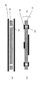
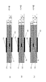
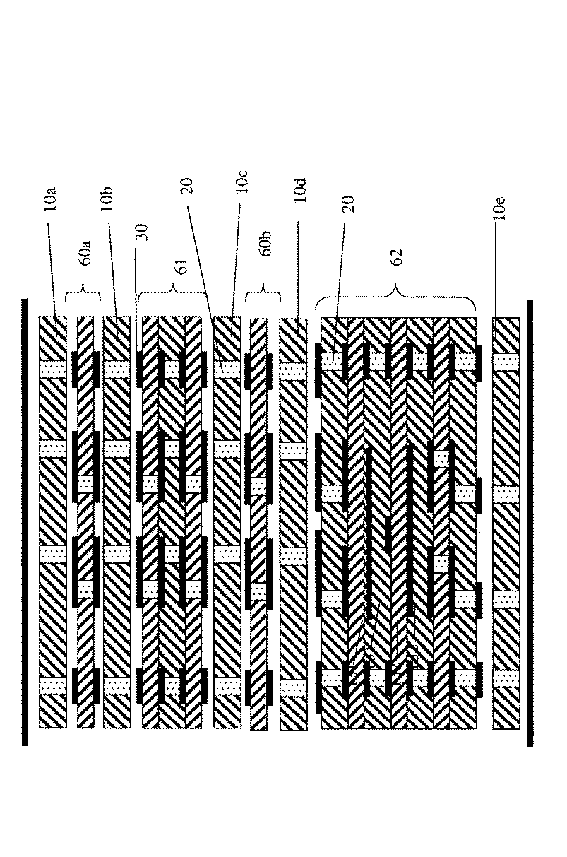
図1、図2を用いて本発明の実施の形態1の多層回路基板の作製手順について説明する。
(数2)
t2=t2′−t0=t1
となることである。誤差を考慮した条件はt2≧t1であるから、(数2)をこれに代入して、
(数3)
t2′≧t1+t0
となる。両面回路基板の基板本体となるプリプレグ131,信号配線S1の厚みは、多層回路基板の製造時の変化を受けることは少ないため、この条件を満たすように、プリプレグ132の厚みt2′を定めればよい。
(数1)
t2′=α・t1+k・t0
で定義すれば、上記(数3)の条件を満たす、特性インピーダンスのばらつきを抑える多層回路基板の製造条件が得られることになる。
2 導電ペースト
3 回路パターン
4a、4b 金属箔(銅箔)
5a、5b 両面回路基板
10、10a、10b、10c、10d、10e プリプレグ
20 導電ペースト
30 回路パターン
40a、40b 金属箔
50、50a、50b、50c、60a、60b 両面回路基板
61 4層回路基板
62 8層回路基板
70a、70b 多層回路基板
G1、G2 接地配線
S1、S2、S3 信号配線
Claims (9)
- 両面に電極線がパターニングされた両面回路基板の少なくとも一方に、所定厚みのプリプレグシートを積層して積層体を作成する工程と、
前記積層体を加熱加圧して、前記両面回路基板と前記プリプレグシートとの境界において前記電極線が前記プリプレグシート内へ埋設されている層構造を完成する工程とを備え、前記層構造を少なくとも一つ内層として含む多層回路基板を製造する多層回路基板の製造方法であって、
前記積層体を作成する前記工程において、
前記積層体を作成する前の段階で、準備すべきプリプレグシートの厚みを、
前記両面回路基板の本体厚みをt1、前記電極線の厚みをt0とする時、t1及びt0に各々独立して比例した厚さを持たせ、かつ、前記層構造を完成する工程において、加熱加圧後の完成した積層体のプリプレグシート厚t2′が、
(数1)
t2′=α(αは1≦α≦1.2を満たす所定値)・t1+k(kは0<k≦1を満たす所定値)・t0
の関係を保つ様に、
作成する、多層回路基板の製造方法。 - 前記(数1)は、t2´=t1+t0
である、請求項1記載の多層回路基板の製造方法。 - 前記所定値αは、1.05である、請求項1記載の多層回路基板の製造方法。
- 前記積層体は、
前記複数の両面回路基板と、他の複数のプリプレグシートを交互に位置決めして重ねる工程により作成し、
前記層構造は、前記積層体の上下の両面を加熱加圧して、前記他の複数のプリプレグシートを硬化させる工程により作成する、請求項1から3のいずれかに記載の多層回路基板の製造方法。 - 前記積層体は、
前記複数の両面回路基板と、他の複数のプリプレグシートを交互に位置決めして重ねる工程により作成し、
前記層構造は、前記積層体の任意の部位を部分的に加熱加圧して、前記他の複数のプリプレグシートが含有している樹脂を溶融させ、その後硬化させて前記回路基板群を接着する工程により作成する、請求項1から3のいずれかに記載の多層回路基板の製造方法。 - 前記積層体は、
前記複数の両面回路基板と前記他の複数のプリプレグシートのいずれかを1枚ずつ重ねることにより複数個作成し、
前記層構造は、前記複数個の積層体を重ね合わせ、それらの任意の部位を部分的に加熱加圧して、前記他の複数のプリプレグシートが含有している樹脂を溶融させ、その後硬化させて相互に接着することにより作成する、請求項1から3のいずれかに記載の多層回路基板の製造方法。 - 前記積層体を作成するための、前記複数の両面回路基板と、他の複数のプリプレグシートを交互に位置決めして重ねる工程は、
最初と最後に銅箔を配置し、前記他の複数のプリプレグシートが前記銅箔に隣接するように配置する工程を有する、請求項4または5記載の多層回路基板の製造方法。 - 前記複数の両面回路基板に代えて、複数の2層以上の回路パターンを有する回路基板を用いる、請求項4から6のいずれかに記載の多層回路基板の製造方法。
- 前記積層体を作成するための工程を、前記複数の両面回路基板と、他の複数のプリプレグシートを交互に位置決めして重ねる工程を、
2層以上の回路パターンを有する2枚の回路基板の間に、1枚のプリプレグシートを挟んで重ね合わせる工程に置換した、請求項4から6のいずれかに記載の多層回路基板の製造方法。
Applications Claiming Priority (1)
| Application Number | Priority Date | Filing Date | Title |
|---|---|---|---|
| PCT/JP2005/001136 WO2006080073A1 (ja) | 2005-01-27 | 2005-01-27 | 多層回路基板の製造方法、多層回路基板 |
Publications (2)
| Publication Number | Publication Date |
|---|---|
| JPWO2006080073A1 JPWO2006080073A1 (ja) | 2008-06-19 |
| JP4819033B2 true JP4819033B2 (ja) | 2011-11-16 |
Family
ID=36740108
Family Applications (1)
| Application Number | Title | Priority Date | Filing Date |
|---|---|---|---|
| JP2007500386A Expired - Fee Related JP4819033B2 (ja) | 2005-01-27 | 2005-01-27 | 多層回路基板の製造方法 |
Country Status (4)
| Country | Link |
|---|---|
| US (1) | US20090032285A1 (ja) |
| JP (1) | JP4819033B2 (ja) |
| CN (1) | CN101120623B (ja) |
| WO (1) | WO2006080073A1 (ja) |
Families Citing this family (17)
| Publication number | Priority date | Publication date | Assignee | Title |
|---|---|---|---|---|
| TWM292164U (en) * | 2005-12-23 | 2006-06-11 | Inpaq Technology Co Ltd | Miniature electronic circuit protection element |
| CN101031182A (zh) * | 2007-03-23 | 2007-09-05 | 华为技术有限公司 | 印制线路板及其设计方法 |
| US8723047B2 (en) * | 2007-03-23 | 2014-05-13 | Huawei Technologies Co., Ltd. | Printed circuit board, design method thereof and mainboard of terminal product |
| US8863046B2 (en) * | 2008-04-11 | 2014-10-14 | International Business Machines Corporation | Controlling impedance and thickness variations for multilayer electronic structures |
| US8549444B2 (en) * | 2008-04-11 | 2013-10-01 | International Business Machines Corporation | Controlling impedance and thickness variations for multilayer electronic structures |
| US20100200949A1 (en) | 2009-02-12 | 2010-08-12 | International Business Machines Corporation | Method for tuning the threshold voltage of a metal gate and high-k device |
| EP2408285B1 (en) * | 2009-03-12 | 2018-11-14 | Tatsuta Electric Wire & Cable Co., Ltd. | Method of manufacturing multilayer printed wiring board and multilayer wiring board obtained thereby |
| JPWO2011155162A1 (ja) * | 2010-06-08 | 2013-08-01 | パナソニック株式会社 | 多層配線基板および多層配線基板の製造方法 |
| KR20120067057A (ko) * | 2010-12-15 | 2012-06-25 | 삼성전자주식회사 | 적어도 하나의 레이어를 포함하는 pcb |
| JP5874697B2 (ja) * | 2013-08-28 | 2016-03-02 | 株式会社デンソー | 多層プリント基板およびその製造方法 |
| US10297571B2 (en) * | 2013-09-06 | 2019-05-21 | Toshiba Memory Corporation | Semiconductor package |
| US9818682B2 (en) * | 2014-12-03 | 2017-11-14 | International Business Machines Corporation | Laminate substrates having radial cut metallic planes |
| JP6627666B2 (ja) * | 2016-07-07 | 2020-01-08 | 株式会社オートネットワーク技術研究所 | 回路基板及び電気接続箱 |
| US10287506B2 (en) * | 2016-11-21 | 2019-05-14 | Beijing Huashi United Energy Technology and Development Co., Ltd | Biomass liquefaction process, and fuel oils and chemical materials prepared by the same |
| KR102410197B1 (ko) * | 2017-06-13 | 2022-06-17 | 삼성전자주식회사 | 전송 손실을 줄이기 위한 회로 기판 및 이를 구비한 전자 장치 |
| EP4081005A1 (en) | 2021-04-23 | 2022-10-26 | AT & S Austria Technologie & Systemtechnik Aktiengesellschaft | Component carrier |
| US20240407105A1 (en) * | 2023-05-31 | 2024-12-05 | International Business Machines Corporation | X-y shielding of signal paths within pcbs |
Citations (7)
| Publication number | Priority date | Publication date | Assignee | Title |
|---|---|---|---|---|
| JPS56144957A (en) * | 1980-04-15 | 1981-11-11 | Matsushita Electric Works Ltd | Manufacture of laminated board for multilayer printed wiring |
| JPH03219692A (ja) * | 1990-01-24 | 1991-09-27 | Shin Kobe Electric Mach Co Ltd | 多層印刷配線板の製造法 |
| JPH0424997A (ja) * | 1990-05-15 | 1992-01-28 | Matsushita Electric Works Ltd | 多層プリント基板の製造方法 |
| JPH07111386A (ja) * | 1993-10-12 | 1995-04-25 | Hitachi Ltd | 多層配線基板およびその製造方法 |
| JPH07249868A (ja) * | 1994-03-09 | 1995-09-26 | Matsushita Electric Ind Co Ltd | 多層基板の製造方法 |
| JP2001007481A (ja) * | 1999-05-26 | 2001-01-12 | Samsung Electro Mech Co Ltd | ラムバス用印刷回路基板 |
| JP2003309378A (ja) * | 2002-04-18 | 2003-10-31 | Mitsubishi Electric Corp | 信号伝送用多層配線板 |
Family Cites Families (34)
| Publication number | Priority date | Publication date | Assignee | Title |
|---|---|---|---|---|
| US4900878A (en) * | 1988-10-03 | 1990-02-13 | Hughes Aircraft Company | Circuit terminations having improved electrical and structural integrity |
| TW210422B (ja) * | 1991-06-04 | 1993-08-01 | Akzo Nv | |
| US5365424A (en) * | 1991-07-10 | 1994-11-15 | Kenetech Windpower, Inc. | High power laminated bus assembly for an electrical switching converter |
| US5219292A (en) * | 1992-04-03 | 1993-06-15 | Motorola, Inc. | Printed circuit board interconnection |
| US5357672A (en) * | 1993-08-13 | 1994-10-25 | Lsi Logic Corporation | Method and system for fabricating IC packages from laminated boards and heat spreader |
| EP0645950B1 (en) * | 1993-09-21 | 1998-09-02 | Matsushita Electric Industrial Co., Ltd. | Connecting member of a circuit substrate and method of manufacturing multilayer circuit substrates by using the same |
| US5499444A (en) * | 1994-08-02 | 1996-03-19 | Coesen, Inc. | Method of manufacturing a rigid flex printed circuit board |
| US5542175A (en) * | 1994-12-20 | 1996-08-06 | International Business Machines Corporation | Method of laminating and circuitizing substrates having openings therein |
| JP3311899B2 (ja) * | 1995-01-20 | 2002-08-05 | 松下電器産業株式会社 | 回路基板及びその製造方法 |
| US5566448A (en) * | 1995-06-06 | 1996-10-22 | International Business Machines Corporation | Method of construction for multi-tiered cavities used in laminate carriers |
| US5906042A (en) * | 1995-10-04 | 1999-05-25 | Prolinx Labs Corporation | Method and structure to interconnect traces of two conductive layers in a printed circuit board |
| EP0805614B1 (en) * | 1995-11-17 | 2005-04-13 | Kabushiki Kaisha Toshiba | Multilayered wiring board, prefabricated material for multilayered wiring board, process of manufacturing multilayered wiring board, electronic parts package, and method for forming conductive pillar |
| US5747358A (en) * | 1996-05-29 | 1998-05-05 | W. L. Gore & Associates, Inc. | Method of forming raised metallic contacts on electrical circuits |
| US6631558B2 (en) * | 1996-06-05 | 2003-10-14 | Laservia Corporation | Blind via laser drilling system |
| US5832596A (en) * | 1996-12-31 | 1998-11-10 | Stmicroelectronics, Inc. | Method of making multiple-bond shelf plastic package |
| US6350387B2 (en) * | 1997-02-14 | 2002-02-26 | Teledyne Industries, Inc. | Multilayer combined rigid/flex printed circuit board containing flexible soldermask |
| US5997983A (en) * | 1997-05-30 | 1999-12-07 | Teledyneindustries, Inc. | Rigid/flex printed circuit board using angled prepreg |
| USRE40947E1 (en) * | 1997-10-14 | 2009-10-27 | Ibiden Co., Ltd. | Multilayer printed wiring board and its manufacturing method, and resin composition for filling through-hole |
| CN101094565A (zh) * | 1997-12-11 | 2007-12-26 | 伊比登株式会社 | 多层印刷电路板的制造方法 |
| US6329899B1 (en) * | 1998-04-29 | 2001-12-11 | Microcoating Technologies, Inc. | Formation of thin film resistors |
| KR100855529B1 (ko) * | 1998-09-03 | 2008-09-01 | 이비덴 가부시키가이샤 | 다층프린트배선판 및 그 제조방법 |
| MY144503A (en) * | 1998-09-14 | 2011-09-30 | Ibiden Co Ltd | Printed circuit board and method for its production |
| US6613413B1 (en) * | 1999-04-26 | 2003-09-02 | International Business Machines Corporation | Porous power and ground planes for reduced PCB delamination and better reliability |
| US6708404B1 (en) * | 1999-06-17 | 2004-03-23 | Mitsubishi Gas Chemical Company, Inc. | Method of producing high-density copper clad multi-layered printed wiring board having highly reliable through hole |
| US6224965B1 (en) * | 1999-06-25 | 2001-05-01 | Honeywell International Inc. | Microfiber dielectrics which facilitate laser via drilling |
| CN1344130A (zh) * | 2000-09-15 | 2002-04-10 | 神达电脑股份有限公司 | 六层电路板压合方法及其成品 |
| US20020162685A1 (en) * | 2001-05-07 | 2002-11-07 | Jeffrey Gotro | Thermal dissipating printed circuit board and methods |
| JP2003078244A (ja) * | 2001-06-18 | 2003-03-14 | Nitto Denko Corp | 多層配線基板及びその製造方法 |
| US20020189091A1 (en) * | 2001-06-19 | 2002-12-19 | Advanced Semiconductor Engineering, Inc. | Method of making printed circuit board |
| JP3985633B2 (ja) * | 2002-08-26 | 2007-10-03 | 株式会社日立製作所 | 低誘電正接絶縁材料を用いた高周波用電子部品 |
| JP4119205B2 (ja) * | 2002-08-27 | 2008-07-16 | 富士通株式会社 | 多層配線基板 |
| US7029971B2 (en) * | 2003-07-17 | 2006-04-18 | E. I. Du Pont De Nemours And Company | Thin film dielectrics for capacitors and methods of making thereof |
| JP2005051075A (ja) * | 2003-07-29 | 2005-02-24 | Matsushita Electric Ind Co Ltd | 多層回路基板およびその製造方法 |
| US7202419B2 (en) * | 2004-07-20 | 2007-04-10 | Dragonwave Inc. | Multi-layer integrated RF/IF circuit board including a central non-conductive layer |
-
2005
- 2005-01-27 WO PCT/JP2005/001136 patent/WO2006080073A1/ja not_active Ceased
- 2005-01-27 JP JP2007500386A patent/JP4819033B2/ja not_active Expired - Fee Related
- 2005-01-27 CN CN2005800472618A patent/CN101120623B/zh not_active Expired - Fee Related
- 2005-01-27 US US11/814,698 patent/US20090032285A1/en not_active Abandoned
Patent Citations (7)
| Publication number | Priority date | Publication date | Assignee | Title |
|---|---|---|---|---|
| JPS56144957A (en) * | 1980-04-15 | 1981-11-11 | Matsushita Electric Works Ltd | Manufacture of laminated board for multilayer printed wiring |
| JPH03219692A (ja) * | 1990-01-24 | 1991-09-27 | Shin Kobe Electric Mach Co Ltd | 多層印刷配線板の製造法 |
| JPH0424997A (ja) * | 1990-05-15 | 1992-01-28 | Matsushita Electric Works Ltd | 多層プリント基板の製造方法 |
| JPH07111386A (ja) * | 1993-10-12 | 1995-04-25 | Hitachi Ltd | 多層配線基板およびその製造方法 |
| JPH07249868A (ja) * | 1994-03-09 | 1995-09-26 | Matsushita Electric Ind Co Ltd | 多層基板の製造方法 |
| JP2001007481A (ja) * | 1999-05-26 | 2001-01-12 | Samsung Electro Mech Co Ltd | ラムバス用印刷回路基板 |
| JP2003309378A (ja) * | 2002-04-18 | 2003-10-31 | Mitsubishi Electric Corp | 信号伝送用多層配線板 |
Also Published As
| Publication number | Publication date |
|---|---|
| JPWO2006080073A1 (ja) | 2008-06-19 |
| CN101120623B (zh) | 2010-07-28 |
| WO2006080073A1 (ja) | 2006-08-03 |
| CN101120623A (zh) | 2008-02-06 |
| US20090032285A1 (en) | 2009-02-05 |
Similar Documents
| Publication | Publication Date | Title |
|---|---|---|
| JP4819033B2 (ja) | 多層回路基板の製造方法 | |
| JP2011159855A (ja) | 局所多層回路基板、および局所多層回路基板の製造方法 | |
| JP4768059B2 (ja) | 多層フレキシブルプリント配線板 | |
| US20170006699A1 (en) | Multilayer circuit board, semiconductor apparatus, and method of manufacturing multilayer circuit board | |
| KR101116079B1 (ko) | 다층 프린트 배선판의 제조방법 및 다층 프린트 배선판 | |
| JP4246615B2 (ja) | フレックスリジッドプリント配線板及びその製造方法 | |
| JP2010123830A (ja) | プリント配線板とその製造方法 | |
| KR20120019144A (ko) | 인쇄회로기판 제조방법 | |
| JP2007149870A (ja) | 回路基板及び回路基板の製造方法。 | |
| JP2005051075A (ja) | 多層回路基板およびその製造方法 | |
| CN207124812U (zh) | 线圈内置基板 | |
| JP2010123829A (ja) | プリント配線板とその製造方法 | |
| JP3879158B2 (ja) | 多層プリント配線板とその製造方法 | |
| JP2014068047A (ja) | 多層プリント配線板の製造方法 | |
| JP2011187854A (ja) | 多層プリント配線板および多層プリント配線板の製造方法 | |
| JP2014192497A (ja) | 配線基板 | |
| KR101138542B1 (ko) | 다층 인쇄회로기판의 제조방법 | |
| JP5293692B2 (ja) | フレックスリジッド配線基板及びその製造方法 | |
| JP3230727B2 (ja) | 多層プリント配線板及びその製造方法 | |
| JP2010205809A (ja) | 多層プリント配線板およびその製造方法 | |
| JP2022083748A (ja) | 配線基板 | |
| TWI911200B (zh) | 電路基板、電路基板的製造方法及電子機器 | |
| JP4899409B2 (ja) | 多層プリント配線基板及びその製造方法 | |
| TWI921489B (zh) | 電路基板之製造方法 | |
| JP5196056B1 (ja) | 複合多層配線基板とその製造方法 |
Legal Events
| Date | Code | Title | Description |
|---|---|---|---|
| A131 | Notification of reasons for refusal |
Free format text: JAPANESE INTERMEDIATE CODE: A131 Effective date: 20100907 |
|
| A521 | Request for written amendment filed |
Free format text: JAPANESE INTERMEDIATE CODE: A523 Effective date: 20101028 |
|
| RD02 | Notification of acceptance of power of attorney |
Free format text: JAPANESE INTERMEDIATE CODE: A7422 Effective date: 20101028 |
|
| A131 | Notification of reasons for refusal |
Free format text: JAPANESE INTERMEDIATE CODE: A131 Effective date: 20110607 |
|
| A521 | Request for written amendment filed |
Free format text: JAPANESE INTERMEDIATE CODE: A523 Effective date: 20110802 |
|
| TRDD | Decision of grant or rejection written | ||
| A01 | Written decision to grant a patent or to grant a registration (utility model) |
Free format text: JAPANESE INTERMEDIATE CODE: A01 Effective date: 20110823 |
|
| A01 | Written decision to grant a patent or to grant a registration (utility model) |
Free format text: JAPANESE INTERMEDIATE CODE: A01 |
|
| A61 | First payment of annual fees (during grant procedure) |
Free format text: JAPANESE INTERMEDIATE CODE: A61 Effective date: 20110831 |
|
| FPAY | Renewal fee payment (event date is renewal date of database) |
Free format text: PAYMENT UNTIL: 20140909 Year of fee payment: 3 |
|
| R150 | Certificate of patent or registration of utility model |
Free format text: JAPANESE INTERMEDIATE CODE: R150 |
|
| LAPS | Cancellation because of no payment of annual fees |