JP4828537B2 - 半導体装置 - Google Patents
半導体装置 Download PDFInfo
- Publication number
- JP4828537B2 JP4828537B2 JP2007532208A JP2007532208A JP4828537B2 JP 4828537 B2 JP4828537 B2 JP 4828537B2 JP 2007532208 A JP2007532208 A JP 2007532208A JP 2007532208 A JP2007532208 A JP 2007532208A JP 4828537 B2 JP4828537 B2 JP 4828537B2
- Authority
- JP
- Japan
- Prior art keywords
- holes
- film
- semiconductor device
- wafer
- main surface
- Prior art date
- Legal status (The legal status is an assumption and is not a legal conclusion. Google has not performed a legal analysis and makes no representation as to the accuracy of the status listed.)
- Expired - Fee Related
Links
Images




Classifications
-
- H—ELECTRICITY
- H10—SEMICONDUCTOR DEVICES; ELECTRIC SOLID-STATE DEVICES NOT OTHERWISE PROVIDED FOR
- H10W—GENERIC PACKAGES, INTERCONNECTIONS, CONNECTORS OR OTHER CONSTRUCTIONAL DETAILS OF DEVICES COVERED BY CLASS H10
- H10W90/00—Package configurations
-
- H—ELECTRICITY
- H10—SEMICONDUCTOR DEVICES; ELECTRIC SOLID-STATE DEVICES NOT OTHERWISE PROVIDED FOR
- H10D—INORGANIC ELECTRIC SEMICONDUCTOR DEVICES
- H10D84/00—Integrated devices formed in or on semiconductor substrates that comprise only semiconducting layers, e.g. on Si wafers or on GaAs-on-Si wafers
- H10D84/01—Manufacture or treatment
- H10D84/0123—Integrating together multiple components covered by H10D12/00 or H10D30/00, e.g. integrating multiple IGBTs
- H10D84/0126—Integrating together multiple components covered by H10D12/00 or H10D30/00, e.g. integrating multiple IGBTs the components including insulated gates, e.g. IGFETs
- H10D84/0165—Integrating together multiple components covered by H10D12/00 or H10D30/00, e.g. integrating multiple IGBTs the components including insulated gates, e.g. IGFETs the components including complementary IGFETs, e.g. CMOS devices
- H10D84/0186—Manufacturing their interconnections or electrodes, e.g. source or drain electrodes
-
- H—ELECTRICITY
- H10—SEMICONDUCTOR DEVICES; ELECTRIC SOLID-STATE DEVICES NOT OTHERWISE PROVIDED FOR
- H10D—INORGANIC ELECTRIC SEMICONDUCTOR DEVICES
- H10D84/00—Integrated devices formed in or on semiconductor substrates that comprise only semiconducting layers, e.g. on Si wafers or on GaAs-on-Si wafers
- H10D84/01—Manufacture or treatment
- H10D84/0123—Integrating together multiple components covered by H10D12/00 or H10D30/00, e.g. integrating multiple IGBTs
- H10D84/0126—Integrating together multiple components covered by H10D12/00 or H10D30/00, e.g. integrating multiple IGBTs the components including insulated gates, e.g. IGFETs
- H10D84/0165—Integrating together multiple components covered by H10D12/00 or H10D30/00, e.g. integrating multiple IGBTs the components including insulated gates, e.g. IGFETs the components including complementary IGFETs, e.g. CMOS devices
- H10D84/0188—Manufacturing their isolation regions
-
- H—ELECTRICITY
- H10—SEMICONDUCTOR DEVICES; ELECTRIC SOLID-STATE DEVICES NOT OTHERWISE PROVIDED FOR
- H10D—INORGANIC ELECTRIC SEMICONDUCTOR DEVICES
- H10D84/00—Integrated devices formed in or on semiconductor substrates that comprise only semiconducting layers, e.g. on Si wafers or on GaAs-on-Si wafers
- H10D84/01—Manufacture or treatment
- H10D84/02—Manufacture or treatment characterised by using material-based technologies
- H10D84/03—Manufacture or treatment characterised by using material-based technologies using Group IV technology, e.g. silicon technology or silicon-carbide [SiC] technology
- H10D84/038—Manufacture or treatment characterised by using material-based technologies using Group IV technology, e.g. silicon technology or silicon-carbide [SiC] technology using silicon technology, e.g. SiGe
-
- H—ELECTRICITY
- H10—SEMICONDUCTOR DEVICES; ELECTRIC SOLID-STATE DEVICES NOT OTHERWISE PROVIDED FOR
- H10D—INORGANIC ELECTRIC SEMICONDUCTOR DEVICES
- H10D89/00—Aspects of integrated devices not covered by groups H10D84/00 - H10D88/00
-
- H—ELECTRICITY
- H10—SEMICONDUCTOR DEVICES; ELECTRIC SOLID-STATE DEVICES NOT OTHERWISE PROVIDED FOR
- H10W—GENERIC PACKAGES, INTERCONNECTIONS, CONNECTORS OR OTHER CONSTRUCTIONAL DETAILS OF DEVICES COVERED BY CLASS H10
- H10W10/00—Isolation regions in semiconductor bodies between components of integrated devices
- H10W10/01—Manufacture or treatment
- H10W10/041—Manufacture or treatment of isolation regions comprising polycrystalline semiconductor materials
-
- H—ELECTRICITY
- H10—SEMICONDUCTOR DEVICES; ELECTRIC SOLID-STATE DEVICES NOT OTHERWISE PROVIDED FOR
- H10W—GENERIC PACKAGES, INTERCONNECTIONS, CONNECTORS OR OTHER CONSTRUCTIONAL DETAILS OF DEVICES COVERED BY CLASS H10
- H10W10/00—Isolation regions in semiconductor bodies between components of integrated devices
- H10W10/40—Isolation regions comprising polycrystalline semiconductor materials
-
- H—ELECTRICITY
- H10—SEMICONDUCTOR DEVICES; ELECTRIC SOLID-STATE DEVICES NOT OTHERWISE PROVIDED FOR
- H10W—GENERIC PACKAGES, INTERCONNECTIONS, CONNECTORS OR OTHER CONSTRUCTIONAL DETAILS OF DEVICES COVERED BY CLASS H10
- H10W20/00—Interconnections in chips, wafers or substrates
- H10W20/01—Manufacture or treatment
- H10W20/021—Manufacture or treatment of interconnections within wafers or substrates
- H10W20/023—Manufacture or treatment of interconnections within wafers or substrates the interconnections being through-semiconductor vias
-
- H—ELECTRICITY
- H10—SEMICONDUCTOR DEVICES; ELECTRIC SOLID-STATE DEVICES NOT OTHERWISE PROVIDED FOR
- H10W—GENERIC PACKAGES, INTERCONNECTIONS, CONNECTORS OR OTHER CONSTRUCTIONAL DETAILS OF DEVICES COVERED BY CLASS H10
- H10W20/00—Interconnections in chips, wafers or substrates
- H10W20/01—Manufacture or treatment
- H10W20/021—Manufacture or treatment of interconnections within wafers or substrates
- H10W20/023—Manufacture or treatment of interconnections within wafers or substrates the interconnections being through-semiconductor vias
- H10W20/0245—Manufacture or treatment of interconnections within wafers or substrates the interconnections being through-semiconductor vias comprising use of blind vias during the manufacture
-
- H—ELECTRICITY
- H10—SEMICONDUCTOR DEVICES; ELECTRIC SOLID-STATE DEVICES NOT OTHERWISE PROVIDED FOR
- H10W—GENERIC PACKAGES, INTERCONNECTIONS, CONNECTORS OR OTHER CONSTRUCTIONAL DETAILS OF DEVICES COVERED BY CLASS H10
- H10W20/00—Interconnections in chips, wafers or substrates
- H10W20/20—Interconnections within wafers or substrates, e.g. through-silicon vias [TSV]
-
- H—ELECTRICITY
- H10—SEMICONDUCTOR DEVICES; ELECTRIC SOLID-STATE DEVICES NOT OTHERWISE PROVIDED FOR
- H10W—GENERIC PACKAGES, INTERCONNECTIONS, CONNECTORS OR OTHER CONSTRUCTIONAL DETAILS OF DEVICES COVERED BY CLASS H10
- H10W20/00—Interconnections in chips, wafers or substrates
- H10W20/20—Interconnections within wafers or substrates, e.g. through-silicon vias [TSV]
- H10W20/211—Through-semiconductor vias, e.g. TSVs
- H10W20/212—Top-view shapes or dispositions, e.g. top-view layouts of the vias
-
- H—ELECTRICITY
- H10—SEMICONDUCTOR DEVICES; ELECTRIC SOLID-STATE DEVICES NOT OTHERWISE PROVIDED FOR
- H10W—GENERIC PACKAGES, INTERCONNECTIONS, CONNECTORS OR OTHER CONSTRUCTIONAL DETAILS OF DEVICES COVERED BY CLASS H10
- H10W20/00—Interconnections in chips, wafers or substrates
- H10W20/20—Interconnections within wafers or substrates, e.g. through-silicon vias [TSV]
- H10W20/211—Through-semiconductor vias, e.g. TSVs
- H10W20/212—Top-view shapes or dispositions, e.g. top-view layouts of the vias
- H10W20/2125—Top-view shapes
-
- H—ELECTRICITY
- H10—SEMICONDUCTOR DEVICES; ELECTRIC SOLID-STATE DEVICES NOT OTHERWISE PROVIDED FOR
- H10W—GENERIC PACKAGES, INTERCONNECTIONS, CONNECTORS OR OTHER CONSTRUCTIONAL DETAILS OF DEVICES COVERED BY CLASS H10
- H10W20/00—Interconnections in chips, wafers or substrates
- H10W20/20—Interconnections within wafers or substrates, e.g. through-silicon vias [TSV]
- H10W20/211—Through-semiconductor vias, e.g. TSVs
- H10W20/213—Cross-sectional shapes or dispositions
- H10W20/2134—TSVs extending from the semiconductor wafer into back-end-of-line layers
-
- H—ELECTRICITY
- H10—SEMICONDUCTOR DEVICES; ELECTRIC SOLID-STATE DEVICES NOT OTHERWISE PROVIDED FOR
- H10W—GENERIC PACKAGES, INTERCONNECTIONS, CONNECTORS OR OTHER CONSTRUCTIONAL DETAILS OF DEVICES COVERED BY CLASS H10
- H10W20/00—Interconnections in chips, wafers or substrates
- H10W20/20—Interconnections within wafers or substrates, e.g. through-silicon vias [TSV]
- H10W20/211—Through-semiconductor vias, e.g. TSVs
- H10W20/217—Through-semiconductor vias, e.g. TSVs comprising ring-shaped isolation structures outside of the via holes
-
- H—ELECTRICITY
- H10—SEMICONDUCTOR DEVICES; ELECTRIC SOLID-STATE DEVICES NOT OTHERWISE PROVIDED FOR
- H10W—GENERIC PACKAGES, INTERCONNECTIONS, CONNECTORS OR OTHER CONSTRUCTIONAL DETAILS OF DEVICES COVERED BY CLASS H10
- H10W72/00—Interconnections or connectors in packages
- H10W72/50—Bond wires
- H10W72/531—Shapes of wire connectors
- H10W72/536—Shapes of wire connectors the connected ends being ball-shaped
-
- H—ELECTRICITY
- H10—SEMICONDUCTOR DEVICES; ELECTRIC SOLID-STATE DEVICES NOT OTHERWISE PROVIDED FOR
- H10W—GENERIC PACKAGES, INTERCONNECTIONS, CONNECTORS OR OTHER CONSTRUCTIONAL DETAILS OF DEVICES COVERED BY CLASS H10
- H10W72/00—Interconnections or connectors in packages
- H10W72/50—Bond wires
- H10W72/531—Shapes of wire connectors
- H10W72/5363—Shapes of wire connectors the connected ends being wedge-shaped
-
- H—ELECTRICITY
- H10—SEMICONDUCTOR DEVICES; ELECTRIC SOLID-STATE DEVICES NOT OTHERWISE PROVIDED FOR
- H10W—GENERIC PACKAGES, INTERCONNECTIONS, CONNECTORS OR OTHER CONSTRUCTIONAL DETAILS OF DEVICES COVERED BY CLASS H10
- H10W72/00—Interconnections or connectors in packages
- H10W72/50—Bond wires
- H10W72/551—Materials of bond wires
- H10W72/552—Materials of bond wires comprising metals or metalloids, e.g. silver
- H10W72/5522—Materials of bond wires comprising metals or metalloids, e.g. silver comprising gold [Au]
-
- H—ELECTRICITY
- H10—SEMICONDUCTOR DEVICES; ELECTRIC SOLID-STATE DEVICES NOT OTHERWISE PROVIDED FOR
- H10W—GENERIC PACKAGES, INTERCONNECTIONS, CONNECTORS OR OTHER CONSTRUCTIONAL DETAILS OF DEVICES COVERED BY CLASS H10
- H10W74/00—Encapsulations, e.g. protective coatings
-
- H—ELECTRICITY
- H10—SEMICONDUCTOR DEVICES; ELECTRIC SOLID-STATE DEVICES NOT OTHERWISE PROVIDED FOR
- H10W—GENERIC PACKAGES, INTERCONNECTIONS, CONNECTORS OR OTHER CONSTRUCTIONAL DETAILS OF DEVICES COVERED BY CLASS H10
- H10W74/00—Encapsulations, e.g. protective coatings
- H10W74/10—Encapsulations, e.g. protective coatings characterised by their shape or disposition
- H10W74/111—Encapsulations, e.g. protective coatings characterised by their shape or disposition the semiconductor body being completely enclosed
- H10W74/114—Encapsulations, e.g. protective coatings characterised by their shape or disposition the semiconductor body being completely enclosed by a substrate and the encapsulations
- H10W74/117—Encapsulations, e.g. protective coatings characterised by their shape or disposition the semiconductor body being completely enclosed by a substrate and the encapsulations the substrate having spherical bumps for external connection
-
- H—ELECTRICITY
- H10—SEMICONDUCTOR DEVICES; ELECTRIC SOLID-STATE DEVICES NOT OTHERWISE PROVIDED FOR
- H10W—GENERIC PACKAGES, INTERCONNECTIONS, CONNECTORS OR OTHER CONSTRUCTIONAL DETAILS OF DEVICES COVERED BY CLASS H10
- H10W90/00—Package configurations
- H10W90/701—Package configurations characterised by the relative positions of pads or connectors relative to package parts
- H10W90/721—Package configurations characterised by the relative positions of pads or connectors relative to package parts of bump connectors
- H10W90/722—Package configurations characterised by the relative positions of pads or connectors relative to package parts of bump connectors between stacked chips
-
- H—ELECTRICITY
- H10—SEMICONDUCTOR DEVICES; ELECTRIC SOLID-STATE DEVICES NOT OTHERWISE PROVIDED FOR
- H10W—GENERIC PACKAGES, INTERCONNECTIONS, CONNECTORS OR OTHER CONSTRUCTIONAL DETAILS OF DEVICES COVERED BY CLASS H10
- H10W90/00—Package configurations
- H10W90/701—Package configurations characterised by the relative positions of pads or connectors relative to package parts
- H10W90/751—Package configurations characterised by the relative positions of pads or connectors relative to package parts of bond wires
- H10W90/754—Package configurations characterised by the relative positions of pads or connectors relative to package parts of bond wires between a chip and a stacked insulating package substrate, interposer or RDL
Landscapes
- Internal Circuitry In Semiconductor Integrated Circuit Devices (AREA)
- Element Separation (AREA)
- Metal-Oxide And Bipolar Metal-Oxide Semiconductor Integrated Circuits (AREA)
- Dicing (AREA)
Description
Claims (9)
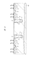
- 主面に形成された複数の第1集積回路素子と、前記主面および裏面を貫通するように形成された複数の第1貫通孔と、前記複数の第1貫通孔のそれぞれの内部に形成され、前記複数の集積回路素子のいずれかに電気的に接続された第1導電膜とを有する第1半導体基板を備えた半導体装置であって、
前記主面における前記複数の第1貫通孔のそれぞれの開口形状は、長方形であり、
前記複数の第1貫通孔は、その長辺が前記主面の第1方向に沿って配向された第1群の貫通孔と、前記長辺が前記主面の第1方向とは異なる第2方向に沿って配向された第2群の貫通孔とを含み、
前記主面における前記第1群の貫通孔の数と前記第2群の貫通孔の数は、等しく、
前記第1群の貫通孔と前記第2群の貫通孔は、電気的に分離されており、
前記第1群の貫通孔の開口形状と前記第2群の貫通孔の開口形状は、等しいことを特徴とする半導体装置。 - 前記主面における前記第1方向と前記第2方向とのなす角は、90度であることを特徴とする請求項1記載の半導体装置。
- 前記主面における前記第1方向と前記第2方向とのなす角は、45度であることを特徴とする請求項1記載の半導体装置。
- 前記複数の第1貫通孔は、それぞれの長辺が同一方向に配向され、かつそれぞれの短辺方向に沿って一列に配列された2個の第1貫通孔を一組とする複数組の貫通孔によって構成されることを特徴とする請求項1記載の半導体装置。
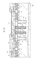
- 主面に複数の第2集積回路素子が形成された第2半導体基板をさらに備え、前記第2半導体基板上に前記第1半導体基板が積層され、前記第1半導体基板の主面に形成された前記第1集積回路素子のいずれかと、前記第2半導体基板の主面に形成された前記第2集積回路素子のいずれかとが、前記複数の第1貫通孔を介して互いに電気的に接続されていることを特徴とする請求項1記載の半導体装置。
- 前記第1半導体基板の厚さと前記第2半導体基板の厚さは異なることを特徴とする請求項5記載の半導体装置。
- 前記第2半導体基板は、その主面および裏面を貫通するように形成された複数の第2貫通孔と、前記複数の第2貫通孔のそれぞれの内部に形成され、前記複数の第2集積回路素子のいずれかに電気的に接続された第2導電膜とをさらに有することを特徴とする請求項5記載の半導体装置。
- 前記第1貫通孔は、短辺の長さが1μm以上であり、深さは短辺の長さの1/2よりも深いことを特徴とする請求項5記載の半導体装置。
- 前記第1導電膜は、タングステンを主成分とする導電膜であることを特徴とする請求項1記載の半導体装置。
Priority Applications (1)
| Application Number | Priority Date | Filing Date | Title |
|---|---|---|---|
| JP2007532208A JP4828537B2 (ja) | 2005-08-26 | 2006-08-25 | 半導体装置 |
Applications Claiming Priority (4)
| Application Number | Priority Date | Filing Date | Title |
|---|---|---|---|
| JP2005245553 | 2005-08-26 | ||
| JP2005245553 | 2005-08-26 | ||
| PCT/JP2006/316770 WO2007023963A1 (ja) | 2005-08-26 | 2006-08-25 | 半導体装置 |
| JP2007532208A JP4828537B2 (ja) | 2005-08-26 | 2006-08-25 | 半導体装置 |
Publications (2)
| Publication Number | Publication Date |
|---|---|
| JPWO2007023963A1 JPWO2007023963A1 (ja) | 2009-03-05 |
| JP4828537B2 true JP4828537B2 (ja) | 2011-11-30 |
Family
ID=37771701
Family Applications (1)
| Application Number | Title | Priority Date | Filing Date |
|---|---|---|---|
| JP2007532208A Expired - Fee Related JP4828537B2 (ja) | 2005-08-26 | 2006-08-25 | 半導体装置 |
Country Status (4)
| Country | Link |
|---|---|
| US (1) | US7948088B2 (ja) |
| JP (1) | JP4828537B2 (ja) |
| TW (1) | TWI407539B (ja) |
| WO (1) | WO2007023963A1 (ja) |
Families Citing this family (11)
| Publication number | Priority date | Publication date | Assignee | Title |
|---|---|---|---|---|
| JP4389227B2 (ja) * | 2006-09-28 | 2009-12-24 | エルピーダメモリ株式会社 | 半導体装置の製造方法 |
| JP2008244187A (ja) * | 2007-03-28 | 2008-10-09 | Elpida Memory Inc | 貫通電極および半導体装置 |
| JP5563186B2 (ja) * | 2007-03-30 | 2014-07-30 | ピーエスフォー ルクスコ エスエイアールエル | 半導体装置及びその製造方法 |
| US8710629B2 (en) | 2009-12-17 | 2014-04-29 | Qualcomm Incorporated | Apparatus and method for controlling semiconductor die warpage |
| CN103378030B (zh) * | 2012-04-18 | 2016-04-20 | 中芯国际集成电路制造(上海)有限公司 | 硅通孔结构 |
| EP2793254B1 (en) * | 2013-04-16 | 2015-10-21 | Ams Ag | Semiconductor device with through-substrate via of enhanced conductivity and corresponding fabrication method |
| JP2016174101A (ja) * | 2015-03-17 | 2016-09-29 | 株式会社東芝 | 半導体装置およびその製造方法 |
| US9543192B2 (en) * | 2015-05-18 | 2017-01-10 | Globalfoundries Singapore Pte. Ltd. | Stitched devices |
| CN106783674B (zh) * | 2016-12-05 | 2019-12-06 | 河北昂扬微电子科技有限公司 | 超薄晶圆翘曲的控制方法 |
| CN113053804B (zh) * | 2021-03-10 | 2023-02-21 | 中国科学院微电子研究所 | 一种钨复合膜层及其生长方法、单片3dic |
| JP7717651B2 (ja) * | 2022-03-21 | 2025-08-04 | 株式会社東芝 | 半導体チップ及び半導体装置 |
Citations (4)
| Publication number | Priority date | Publication date | Assignee | Title |
|---|---|---|---|---|
| JP2002043502A (ja) * | 2000-07-25 | 2002-02-08 | Toshiba Corp | マルチチップ半導体装置、ならびにマルチチップ半導体装置用チップ及びその製造方法 |
| JP2004179673A (ja) * | 2001-05-30 | 2004-06-24 | Sharp Corp | 半導体装置の製造方法 |
| JP2004221430A (ja) * | 2003-01-16 | 2004-08-05 | Nec Electronics Corp | 半導体装置およびそのマスクパターン |
| JP2006165025A (ja) * | 2004-12-02 | 2006-06-22 | Nec Electronics Corp | 半導体装置およびそれを用いた半導体モジュール、ならびに半導体装置の製造方法 |
Family Cites Families (8)
| Publication number | Priority date | Publication date | Assignee | Title |
|---|---|---|---|---|
| JPH11261000A (ja) | 1998-03-13 | 1999-09-24 | Japan Science & Technology Corp | 3次元半導体集積回路装置の製造方法 |
| JP2002124517A (ja) * | 2000-10-13 | 2002-04-26 | Sharp Corp | 半導体装置およびその製造方法 |
| JP2002151796A (ja) * | 2000-11-13 | 2002-05-24 | Sharp Corp | 窒化物半導体発光素子とこれを含む装置 |
| JP2002334967A (ja) | 2001-05-07 | 2002-11-22 | Sony Corp | 3次元半導体チップ |
| US7095114B2 (en) * | 2001-05-30 | 2006-08-22 | Sharp Kabushiki Kaisha | Semiconductor device with via hole group generating high frequency electromagnetic bonding, manufacturing method thereof, and monolithic microwave integrated circuit |
| JP4190211B2 (ja) * | 2002-06-05 | 2008-12-03 | 株式会社東京精密 | 基板加工方法および基板加工装置 |
| JP2005085963A (ja) * | 2003-09-08 | 2005-03-31 | Sharp Corp | 半導体装置およびその製造方法 |
| US7767493B2 (en) * | 2005-06-14 | 2010-08-03 | John Trezza | Post & penetration interconnection |
-
2006
- 2006-08-25 US US12/063,606 patent/US7948088B2/en not_active Expired - Fee Related
- 2006-08-25 TW TW095131381A patent/TWI407539B/zh not_active IP Right Cessation
- 2006-08-25 JP JP2007532208A patent/JP4828537B2/ja not_active Expired - Fee Related
- 2006-08-25 WO PCT/JP2006/316770 patent/WO2007023963A1/ja not_active Ceased
Patent Citations (4)
| Publication number | Priority date | Publication date | Assignee | Title |
|---|---|---|---|---|
| JP2002043502A (ja) * | 2000-07-25 | 2002-02-08 | Toshiba Corp | マルチチップ半導体装置、ならびにマルチチップ半導体装置用チップ及びその製造方法 |
| JP2004179673A (ja) * | 2001-05-30 | 2004-06-24 | Sharp Corp | 半導体装置の製造方法 |
| JP2004221430A (ja) * | 2003-01-16 | 2004-08-05 | Nec Electronics Corp | 半導体装置およびそのマスクパターン |
| JP2006165025A (ja) * | 2004-12-02 | 2006-06-22 | Nec Electronics Corp | 半導体装置およびそれを用いた半導体モジュール、ならびに半導体装置の製造方法 |
Also Published As
| Publication number | Publication date |
|---|---|
| US20090174080A1 (en) | 2009-07-09 |
| TWI407539B (zh) | 2013-09-01 |
| US7948088B2 (en) | 2011-05-24 |
| TW200725865A (en) | 2007-07-01 |
| WO2007023963A1 (ja) | 2007-03-01 |
| JPWO2007023963A1 (ja) | 2009-03-05 |
Similar Documents
| Publication | Publication Date | Title |
|---|---|---|
| JP4916444B2 (ja) | 半導体装置の製造方法 | |
| CN102790017B (zh) | 半导体部件和制造半导体部件的方法 | |
| US11521937B2 (en) | Package structures with built-in EMI shielding | |
| US7812457B2 (en) | Semiconductor device and semiconductor wafer and a method for manufacturing the same | |
| JP2008091852A (ja) | 積層パッケージおよびその製造方法 | |
| CN210805772U (zh) | 半导体装置 | |
| JP2009152583A (ja) | 半導体素子及びその製造方法 | |
| US11309249B2 (en) | Semiconductor package with air gap and manufacturing method thereof | |
| JP2009055004A (ja) | 貫通配線構造 | |
| CN103137566B (zh) | 用于形成集成电路的方法 | |
| WO2010035375A1 (ja) | 半導体装置及びその製造方法 | |
| KR102804065B1 (ko) | 반도체 패키지 및 반도체 패키지의 제조 방법 | |
| US8354730B2 (en) | Manufacturing method of semiconductor device and semiconductor device | |
| JP4828537B2 (ja) | 半導体装置 | |
| JP4945545B2 (ja) | 半導体装置の製造方法 | |
| JP2015099827A (ja) | 半導体装置および半導体装置の製造方法 | |
| US7535062B2 (en) | Semiconductor device having SOI structure | |
| JP5271562B2 (ja) | 半導体装置および半導体装置の製造方法 | |
| CN108807197A (zh) | 具有侧壁金属化部的芯片封装 | |
| JP2018088487A (ja) | 半導体装置及びその製造方法 | |
| JP4696152B2 (ja) | 半導体装置の製造方法および半導体装置 | |
| WO2010082248A1 (ja) | 半導体装置およびそれを用いた電子機器ならびに半導体装置の製造方法 | |
| WO2011148444A1 (ja) | 半導体装置及びその製造方法 |
Legal Events
| Date | Code | Title | Description |
|---|---|---|---|
| A131 | Notification of reasons for refusal |
Free format text: JAPANESE INTERMEDIATE CODE: A131 Effective date: 20100921 |
|
| A521 | Request for written amendment filed |
Free format text: JAPANESE INTERMEDIATE CODE: A523 Effective date: 20101119 |
|
| TRDD | Decision of grant or rejection written | ||
| A01 | Written decision to grant a patent or to grant a registration (utility model) |
Free format text: JAPANESE INTERMEDIATE CODE: A01 Effective date: 20110823 |
|
| A01 | Written decision to grant a patent or to grant a registration (utility model) |
Free format text: JAPANESE INTERMEDIATE CODE: A01 |
|
| A61 | First payment of annual fees (during grant procedure) |
Free format text: JAPANESE INTERMEDIATE CODE: A61 Effective date: 20110914 |
|
| FPAY | Renewal fee payment (event date is renewal date of database) |
Free format text: PAYMENT UNTIL: 20140922 Year of fee payment: 3 |
|
| R150 | Certificate of patent or registration of utility model |
Free format text: JAPANESE INTERMEDIATE CODE: R150 |
|
| LAPS | Cancellation because of no payment of annual fees |