JP4832477B2 - リソグラフィ投影装置及び偏光器デバイス - Google Patents
リソグラフィ投影装置及び偏光器デバイス Download PDFInfo
- Publication number
- JP4832477B2 JP4832477B2 JP2008188601A JP2008188601A JP4832477B2 JP 4832477 B2 JP4832477 B2 JP 4832477B2 JP 2008188601 A JP2008188601 A JP 2008188601A JP 2008188601 A JP2008188601 A JP 2008188601A JP 4832477 B2 JP4832477 B2 JP 4832477B2
- Authority
- JP
- Japan
- Prior art keywords
- polarization
- radiation
- polarizer
- polarizer device
- absorber
- Prior art date
- Legal status (The legal status is an assumption and is not a legal conclusion. Google has not performed a legal analysis and makes no representation as to the accuracy of the status listed.)
- Expired - Fee Related
Links
- 230000010287 polarization Effects 0.000 claims description 171
- 230000005855 radiation Effects 0.000 claims description 60
- 239000000758 substrate Substances 0.000 claims description 51
- 239000000463 material Substances 0.000 claims description 42
- 239000006096 absorbing agent Substances 0.000 claims description 41
- 238000000034 method Methods 0.000 claims description 36
- 238000000059 patterning Methods 0.000 claims description 18
- 230000008569 process Effects 0.000 claims description 14
- 230000003287 optical effect Effects 0.000 claims description 13
- 230000005670 electromagnetic radiation Effects 0.000 claims description 12
- 230000002745 absorbent Effects 0.000 claims description 6
- 239000002250 absorbent Substances 0.000 claims description 6
- 239000011358 absorbing material Substances 0.000 claims description 5
- 230000005540 biological transmission Effects 0.000 claims description 4
- 239000010410 layer Substances 0.000 description 44
- 238000001459 lithography Methods 0.000 description 24
- 238000005516 engineering process Methods 0.000 description 14
- 238000003384 imaging method Methods 0.000 description 14
- 238000005286 illumination Methods 0.000 description 13
- 238000004519 manufacturing process Methods 0.000 description 12
- VYPSYNLAJGMNEJ-UHFFFAOYSA-N silicon dioxide Inorganic materials O=[Si]=O VYPSYNLAJGMNEJ-UHFFFAOYSA-N 0.000 description 11
- 238000010586 diagram Methods 0.000 description 9
- 210000001747 pupil Anatomy 0.000 description 9
- 230000000694 effects Effects 0.000 description 8
- 230000006870 function Effects 0.000 description 7
- 238000000671 immersion lithography Methods 0.000 description 7
- 238000007654 immersion Methods 0.000 description 6
- 230000010363 phase shift Effects 0.000 description 6
- 239000010409 thin film Substances 0.000 description 6
- 230000008033 biological extinction Effects 0.000 description 5
- 239000010408 film Substances 0.000 description 5
- 239000007788 liquid Substances 0.000 description 5
- 238000010791 quenching Methods 0.000 description 5
- 230000000171 quenching effect Effects 0.000 description 5
- VYZAMTAEIAYCRO-UHFFFAOYSA-N Chromium Chemical compound [Cr] VYZAMTAEIAYCRO-UHFFFAOYSA-N 0.000 description 4
- XUIMIQQOPSSXEZ-UHFFFAOYSA-N Silicon Chemical compound [Si] XUIMIQQOPSSXEZ-UHFFFAOYSA-N 0.000 description 4
- 229910052782 aluminium Inorganic materials 0.000 description 4
- XAGFODPZIPBFFR-UHFFFAOYSA-N aluminium Chemical compound [Al] XAGFODPZIPBFFR-UHFFFAOYSA-N 0.000 description 4
- 230000000052 comparative effect Effects 0.000 description 4
- 238000009826 distribution Methods 0.000 description 4
- 229920002120 photoresistant polymer Polymers 0.000 description 4
- 229920000642 polymer Polymers 0.000 description 4
- 229910052710 silicon Inorganic materials 0.000 description 4
- 239000010703 silicon Substances 0.000 description 4
- 235000012239 silicon dioxide Nutrition 0.000 description 4
- 229910052709 silver Inorganic materials 0.000 description 4
- 239000004332 silver Substances 0.000 description 4
- 238000001429 visible spectrum Methods 0.000 description 4
- JBRZTFJDHDCESZ-UHFFFAOYSA-N AsGa Chemical compound [As]#[Ga] JBRZTFJDHDCESZ-UHFFFAOYSA-N 0.000 description 3
- 229910001218 Gallium arsenide Inorganic materials 0.000 description 3
- BQCADISMDOOEFD-UHFFFAOYSA-N Silver Chemical compound [Ag] BQCADISMDOOEFD-UHFFFAOYSA-N 0.000 description 3
- 230000008859 change Effects 0.000 description 3
- 239000011248 coating agent Substances 0.000 description 3
- 238000000576 coating method Methods 0.000 description 3
- 150000001875 compounds Chemical class 0.000 description 3
- 238000013461 design Methods 0.000 description 3
- 238000011161 development Methods 0.000 description 3
- 238000010894 electron beam technology Methods 0.000 description 3
- 239000005350 fused silica glass Substances 0.000 description 3
- 239000011521 glass Substances 0.000 description 3
- PCHJSUWPFVWCPO-UHFFFAOYSA-N gold Chemical compound [Au] PCHJSUWPFVWCPO-UHFFFAOYSA-N 0.000 description 3
- 229910052737 gold Inorganic materials 0.000 description 3
- 239000010931 gold Substances 0.000 description 3
- 239000011159 matrix material Substances 0.000 description 3
- 230000000737 periodic effect Effects 0.000 description 3
- 238000000206 photolithography Methods 0.000 description 3
- 238000007639 printing Methods 0.000 description 3
- 239000000126 substance Substances 0.000 description 3
- 229910052581 Si3N4 Inorganic materials 0.000 description 2
- 229910004298 SiO 2 Inorganic materials 0.000 description 2
- 238000003491 array Methods 0.000 description 2
- 229910052804 chromium Inorganic materials 0.000 description 2
- 239000011651 chromium Substances 0.000 description 2
- 230000001427 coherent effect Effects 0.000 description 2
- 239000004020 conductor Substances 0.000 description 2
- 239000003989 dielectric material Substances 0.000 description 2
- 230000005684 electric field Effects 0.000 description 2
- 230000007613 environmental effect Effects 0.000 description 2
- 230000006872 improvement Effects 0.000 description 2
- 230000007246 mechanism Effects 0.000 description 2
- 238000012986 modification Methods 0.000 description 2
- 230000004048 modification Effects 0.000 description 2
- 239000010453 quartz Substances 0.000 description 2
- 238000002310 reflectometry Methods 0.000 description 2
- 239000000377 silicon dioxide Substances 0.000 description 2
- HQVNEWCFYHHQES-UHFFFAOYSA-N silicon nitride Chemical compound N12[Si]34N5[Si]62N3[Si]51N64 HQVNEWCFYHHQES-UHFFFAOYSA-N 0.000 description 2
- 238000004088 simulation Methods 0.000 description 2
- 239000002356 single layer Substances 0.000 description 2
- 239000007787 solid Substances 0.000 description 2
- 238000001228 spectrum Methods 0.000 description 2
- XLYOFNOQVPJJNP-UHFFFAOYSA-N water Substances O XLYOFNOQVPJJNP-UHFFFAOYSA-N 0.000 description 2
- ZCYVEMRRCGMTRW-UHFFFAOYSA-N 7553-56-2 Chemical compound [I] ZCYVEMRRCGMTRW-UHFFFAOYSA-N 0.000 description 1
- 229910018072 Al 2 O 3 Inorganic materials 0.000 description 1
- 238000010521 absorption reaction Methods 0.000 description 1
- 230000004075 alteration Effects 0.000 description 1
- 230000002238 attenuated effect Effects 0.000 description 1
- 239000002131 composite material Substances 0.000 description 1
- 238000005094 computer simulation Methods 0.000 description 1
- 238000010276 construction Methods 0.000 description 1
- 230000008878 coupling Effects 0.000 description 1
- 238000010168 coupling process Methods 0.000 description 1
- 238000005859 coupling reaction Methods 0.000 description 1
- 239000013078 crystal Substances 0.000 description 1
- 238000005520 cutting process Methods 0.000 description 1
- 230000007423 decrease Effects 0.000 description 1
- 230000007547 defect Effects 0.000 description 1
- 230000001419 dependent effect Effects 0.000 description 1
- 238000001514 detection method Methods 0.000 description 1
- 230000009977 dual effect Effects 0.000 description 1
- 230000008030 elimination Effects 0.000 description 1
- 238000003379 elimination reaction Methods 0.000 description 1
- 238000005530 etching Methods 0.000 description 1
- 238000001900 extreme ultraviolet lithography Methods 0.000 description 1
- 238000007689 inspection Methods 0.000 description 1
- 230000010354 integration Effects 0.000 description 1
- 229910052740 iodine Inorganic materials 0.000 description 1
- 239000011630 iodine Substances 0.000 description 1
- 238000005468 ion implantation Methods 0.000 description 1
- 238000010884 ion-beam technique Methods 0.000 description 1
- 239000002346 layers by function Substances 0.000 description 1
- 239000004973 liquid crystal related substance Substances 0.000 description 1
- 230000005381 magnetic domain Effects 0.000 description 1
- 238000005259 measurement Methods 0.000 description 1
- 238000000691 measurement method Methods 0.000 description 1
- QSHDDOUJBYECFT-UHFFFAOYSA-N mercury Chemical compound [Hg] QSHDDOUJBYECFT-UHFFFAOYSA-N 0.000 description 1
- 229910052753 mercury Inorganic materials 0.000 description 1
- 229910052751 metal Inorganic materials 0.000 description 1
- 239000002184 metal Substances 0.000 description 1
- 238000001465 metallisation Methods 0.000 description 1
- 238000001393 microlithography Methods 0.000 description 1
- 239000000203 mixture Substances 0.000 description 1
- 238000012634 optical imaging Methods 0.000 description 1
- 230000003647 oxidation Effects 0.000 description 1
- 238000007254 oxidation reaction Methods 0.000 description 1
- 239000002245 particle Substances 0.000 description 1
- 238000001020 plasma etching Methods 0.000 description 1
- 238000005498 polishing Methods 0.000 description 1
- 229920006254 polymer film Polymers 0.000 description 1
- 239000002861 polymer material Substances 0.000 description 1
- 230000037452 priming Effects 0.000 description 1
- 238000012545 processing Methods 0.000 description 1
- 239000004065 semiconductor Substances 0.000 description 1
- 230000035945 sensitivity Effects 0.000 description 1
- 229910052814 silicon oxide Inorganic materials 0.000 description 1
- 230000009897 systematic effect Effects 0.000 description 1
- 230000007704 transition Effects 0.000 description 1
Images





Classifications
-
- G—PHYSICS
- G03—PHOTOGRAPHY; CINEMATOGRAPHY; ANALOGOUS TECHNIQUES USING WAVES OTHER THAN OPTICAL WAVES; ELECTROGRAPHY; HOLOGRAPHY
- G03F—PHOTOMECHANICAL PRODUCTION OF TEXTURED OR PATTERNED SURFACES, e.g. FOR PRINTING, FOR PROCESSING OF SEMICONDUCTOR DEVICES; MATERIALS THEREFOR; ORIGINALS THEREFOR; APPARATUS SPECIALLY ADAPTED THEREFOR
- G03F7/00—Photomechanical, e.g. photolithographic, production of textured or patterned surfaces, e.g. printing surfaces; Materials therefor, e.g. comprising photoresists; Apparatus specially adapted therefor
- G03F7/70—Microphotolithographic exposure; Apparatus therefor
- G03F7/70483—Information management; Active and passive control; Testing; Wafer monitoring, e.g. pattern monitoring
- G03F7/7055—Exposure light control in all parts of the microlithographic apparatus, e.g. pulse length control or light interruption
- G03F7/70566—Polarisation control
-
- G—PHYSICS
- G02—OPTICS
- G02B—OPTICAL ELEMENTS, SYSTEMS OR APPARATUS
- G02B5/00—Optical elements other than lenses
- G02B5/30—Polarising elements
- G02B5/3025—Polarisers, i.e. arrangements capable of producing a definite output polarisation state from an unpolarised input state
- G02B5/3058—Polarisers, i.e. arrangements capable of producing a definite output polarisation state from an unpolarised input state comprising electrically conductive elements, e.g. wire grids, conductive particles
Landscapes
- Physics & Mathematics (AREA)
- General Physics & Mathematics (AREA)
- Optics & Photonics (AREA)
- Exposure And Positioning Against Photoresist Photosensitive Materials (AREA)
- Polarising Elements (AREA)
- Exposure Of Semiconductors, Excluding Electron Or Ion Beam Exposure (AREA)
Description
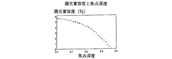
解像度=k1(λ/NA)
及び
DOF=k2(λ/NA2)
ここでλは照明ソースの波長であり、k1及びk2は、特定のリソグラフィ・プロセスの定数である。

ATE=cosθ及びATM=ejφsinθ
Claims (13)
- 横方向磁気偏光及び横方向電気偏光を有する放射線の投影ビームを提供するよう構成された放射線システムと、
パターニング・デバイスを支持するように構成された支持構造であって、前記パターニング・デバイスは、所望のパターンに従って投影ビームにパターン形成するように構成された支持構造と、
基板を保持するよう構成された基板テーブルと、
パターン形成した投影ビームを基板の標的部分に投影するよう構成された投影システムと、
前記投影ビームの光路に配置された偏光器デバイスと、
前記偏光器デバイスを被覆する吸収体と、を備え、
前記偏光器デバイスは、方位角で配向された複数の細長い要素を備え、前記複数の細長い要素は、周期的に隔置されて複数のギャップを形成しており、
前記偏光器デバイスは、前記投影ビームと相互作用して横方向磁気偏光の放射線をほぼ全て反射し、横方向電気偏光の放射線をほぼ全て透過し、
前記吸収体は、前記偏光器デバイスから前記パターニング・デバイスに戻って反射する過程で横方向電気偏光に変化した横方向磁気偏光を吸収する、リソグラフィ投影装置。 - 偏光器デバイスであって、
第1屈折率を有する基板材料と、
前記基板材料に結合され、方位角で配向された、第2屈折率を有する複数の細長い要素と、
前記複数の細長い要素を被覆する吸収性材料の薄い層と、を備え、
前記複数の細長い要素は、周期的に隔置されて複数のギャップを形成し、
前記偏光器デバイスは、第1及び第2偏光を備えた電磁放射線と相互作用して第1偏光の放射線をほぼ全て反射し、第2偏光の放射線をほぼ全て透過し、
前記吸収性材料の薄い層は、前記第2偏光に変化した前記第1偏光の反射放射線を吸収する、偏光器デバイス。 - 前記第2偏光に変化した前記第1偏光の放射線の一部は、前記吸収性材料の薄い層によってほぼ吸収される、請求項2に記載の偏光器デバイス。
- 前記第2偏光に変化した前記第1偏光の放射線は、前記吸収性材料の薄い層によって最少量だけ吸収される、請求項2又は請求項3に記載の偏光器デバイス。
- 前記吸収性材料の薄い層は、前記第2偏光の透過放射線にある偏光のフレアをほぼ解消する、請求項2乃至請求項4のうち何れか1項に記載の偏光器デバイス。
- リソグラフィ投影装置であって、
前記電磁放射線の投影ビームを提供するよう構成された放射線システムと、
パターニング・デバイスを支持するように構成された支持構造であって、前記パターニング・デバイスは、所望のパターンに従って投影ビームにパターン形成するように構成された支持構造と、
基板を保持するよう構成された基板テーブルと、
パターン形成した投影ビームを基板の標的部分に投影するよう構成された投影システムと、
前記投影ビームを前記第2偏光の方向で偏光するよう構築され、配置された請求項2乃至請求項5のうち何れか1項に記載の偏光器デバイスと、
を備えるリソグラフィ投影装置。 - 偏光器デバイスであって、
偏光コンポーネントと、
前記偏光コンポーネントの後方に配置された吸収体と、を備え、
前記偏光コンポーネントは、方位角で配向された複数の細長い要素を備え、前記複数の細長い要素は、周期的に隔置されて複数のギャップを形成しており、
前記偏光コンポーネントは、第1及び第2偏光を備えた電磁放射線と相互作用して第1偏光の放射線をほぼ全て反射し、第2偏光の放射線をほぼ全て透過し、
前記吸収体は、前記第2偏光に変化した前記第1偏光の放射線をほぼ全て吸収する、偏光器デバイス。 - 前記複数の細長い要素は、電磁放射線の波長で導電性である、請求項7に記載の偏光器デバイス。
- 前記第1偏光は、横方向磁気偏光であり、前記第2偏光が横方向電気偏光である、請求項7乃至請求項8のうち何れか1項に記載の偏光器デバイス。
- 前記偏光コンポーネントは、同心円上に配置された複数のリングを備え、
前記リングが周期的に隔置される、請求項7乃至請求項9のうち何れか1項に記載の偏光器デバイス。 - 前記第2偏光の放射線は、前記吸収体によって最少量だけ吸収される、請求項7乃至請求項10のうち何れか1項に記載の偏光器デバイス。
- 前記吸収体は、前記第2偏光の透過放射線にある偏光のフレアをほぼ解消する、請求項7乃至請求項11のうち何れか1項に記載の偏光器デバイス。
- 前記吸収体の厚さは、前記第2偏光に変化した前記第1偏光の放射線を吸収できるように調節されている、請求項7乃至請求項12のうち何れか1項に記載の偏光器デバイス。
Applications Claiming Priority (2)
| Application Number | Priority Date | Filing Date | Title |
|---|---|---|---|
| US374509 | 2003-02-27 | ||
| US10/374,509 US6943941B2 (en) | 2003-02-27 | 2003-02-27 | Stationary and dynamic radial transverse electric polarizer for high numerical aperture systems |
Related Parent Applications (1)
| Application Number | Title | Priority Date | Filing Date |
|---|---|---|---|
| JP2004090530A Division JP2004258670A (ja) | 2003-02-27 | 2004-02-27 | 高開口数システムの固定および動的ラジアル横方向電気偏光器 |
Publications (2)
| Publication Number | Publication Date |
|---|---|
| JP2009009143A JP2009009143A (ja) | 2009-01-15 |
| JP4832477B2 true JP4832477B2 (ja) | 2011-12-07 |
Family
ID=32907741
Family Applications (2)
| Application Number | Title | Priority Date | Filing Date |
|---|---|---|---|
| JP2004090530A Pending JP2004258670A (ja) | 2003-02-27 | 2004-02-27 | 高開口数システムの固定および動的ラジアル横方向電気偏光器 |
| JP2008188601A Expired - Fee Related JP4832477B2 (ja) | 2003-02-27 | 2008-07-22 | リソグラフィ投影装置及び偏光器デバイス |
Family Applications Before (1)
| Application Number | Title | Priority Date | Filing Date |
|---|---|---|---|
| JP2004090530A Pending JP2004258670A (ja) | 2003-02-27 | 2004-02-27 | 高開口数システムの固定および動的ラジアル横方向電気偏光器 |
Country Status (2)
| Country | Link |
|---|---|
| US (3) | US6943941B2 (ja) |
| JP (2) | JP2004258670A (ja) |
Families Citing this family (163)
| Publication number | Priority date | Publication date | Assignee | Title |
|---|---|---|---|---|
| US20050134825A1 (en) * | 2002-02-08 | 2005-06-23 | Carl Zeiss Smt Ag | Polarization-optimized illumination system |
| US9482966B2 (en) | 2002-11-12 | 2016-11-01 | Asml Netherlands B.V. | Lithographic apparatus and device manufacturing method |
| US10503084B2 (en) | 2002-11-12 | 2019-12-10 | Asml Netherlands B.V. | Lithographic apparatus and device manufacturing method |
| TWI251127B (en) | 2002-11-12 | 2006-03-11 | Asml Netherlands Bv | Lithographic apparatus and device manufacturing method |
| SG2010050110A (en) * | 2002-11-12 | 2014-06-27 | Asml Netherlands Bv | Lithographic apparatus and device manufacturing method |
| US7372541B2 (en) * | 2002-11-12 | 2008-05-13 | Asml Netherlands B.V. | Lithographic apparatus and device manufacturing method |
| CN1723541B (zh) * | 2002-12-10 | 2010-06-02 | 株式会社尼康 | 曝光装置和器件制造方法 |
| SG171468A1 (en) * | 2002-12-10 | 2011-06-29 | Nikon Corp | Exposure apparatus and method for producing device |
| US7242455B2 (en) * | 2002-12-10 | 2007-07-10 | Nikon Corporation | Exposure apparatus and method for producing device |
| EP1571698A4 (en) * | 2002-12-10 | 2006-06-21 | Nikon Corp | EXPOSURE DEVICE, EXPOSURE METHOD AND METHOD FOR PRODUCING COMPONENTS |
| CN101872135B (zh) * | 2002-12-10 | 2013-07-31 | 株式会社尼康 | 曝光设备和器件制造法 |
| JP4352874B2 (ja) * | 2002-12-10 | 2009-10-28 | 株式会社ニコン | 露光装置及びデバイス製造方法 |
| US7948604B2 (en) * | 2002-12-10 | 2011-05-24 | Nikon Corporation | Exposure apparatus and method for producing device |
| DE10261775A1 (de) | 2002-12-20 | 2004-07-01 | Carl Zeiss Smt Ag | Vorrichtung zur optischen Vermessung eines Abbildungssystems |
| KR101506408B1 (ko) | 2003-02-26 | 2015-03-26 | 가부시키가이샤 니콘 | 노광 장치, 노광 방법 및 디바이스 제조 방법 |
| US6943941B2 (en) * | 2003-02-27 | 2005-09-13 | Asml Netherlands B.V. | Stationary and dynamic radial transverse electric polarizer for high numerical aperture systems |
| US7206059B2 (en) * | 2003-02-27 | 2007-04-17 | Asml Netherlands B.V. | Stationary and dynamic radial transverse electric polarizer for high numerical aperture systems |
| EP1610361B1 (en) | 2003-03-25 | 2014-05-21 | Nikon Corporation | Exposure system and device production method |
| KR101176817B1 (ko) | 2003-04-07 | 2012-08-24 | 가부시키가이샤 니콘 | 노광장치 및 디바이스 제조방법 |
| KR20170018113A (ko) | 2003-04-09 | 2017-02-15 | 가부시키가이샤 니콘 | 노광 방법 및 장치, 그리고 디바이스 제조 방법 |
| WO2004093159A2 (en) * | 2003-04-09 | 2004-10-28 | Nikon Corporation | Immersion lithography fluid control system |
| WO2004093160A2 (en) | 2003-04-10 | 2004-10-28 | Nikon Corporation | Run-off path to collect liquid for an immersion lithography apparatus |
| EP3062152B1 (en) | 2003-04-10 | 2017-12-20 | Nikon Corporation | Environmental system including vaccum scavenge for an immersion lithography apparatus |
| JP4656057B2 (ja) * | 2003-04-10 | 2011-03-23 | 株式会社ニコン | 液浸リソグラフィ装置用電気浸透素子 |
| KR20180089562A (ko) * | 2003-04-10 | 2018-08-08 | 가부시키가이샤 니콘 | 액침 리소그래피 장치용 진공 배출을 포함하는 환경 시스템 |
| JP4582089B2 (ja) | 2003-04-11 | 2010-11-17 | 株式会社ニコン | 液浸リソグラフィ用の液体噴射回収システム |
| JP4315198B2 (ja) | 2003-04-11 | 2009-08-19 | 株式会社ニコン | 液浸液体を光学アセンブリ下に維持するリソグラフィ装置及び液浸液体維持方法並びにそれらを用いるデバイス製造方法 |
| KR101324818B1 (ko) | 2003-04-11 | 2013-11-01 | 가부시키가이샤 니콘 | 액침 리소그래피에 의한 광학기기의 세정방법 |
| CN1774667A (zh) | 2003-04-17 | 2006-05-17 | 株式会社尼康 | 用在浸没式平版印刷方法中自动聚焦部件的光学配置 |
| TWI295414B (en) * | 2003-05-13 | 2008-04-01 | Asml Netherlands Bv | Lithographic apparatus and device manufacturing method |
| WO2004102646A1 (ja) * | 2003-05-15 | 2004-11-25 | Nikon Corporation | 露光装置及びデバイス製造方法 |
| TWI518742B (zh) * | 2003-05-23 | 2016-01-21 | 尼康股份有限公司 | A method of manufacturing an exposure apparatus and an element |
| TWI511181B (zh) * | 2003-05-23 | 2015-12-01 | 尼康股份有限公司 | Exposure method and exposure apparatus, and device manufacturing method |
| KR20180122033A (ko) * | 2003-05-28 | 2018-11-09 | 가부시키가이샤 니콘 | 노광 방법, 노광 장치, 및 디바이스 제조 방법 |
| DE10324477A1 (de) * | 2003-05-30 | 2004-12-30 | Carl Zeiss Smt Ag | Mikrolithographische Projektionsbelichtungsanlage |
| DE10324468B4 (de) * | 2003-05-30 | 2006-11-09 | Carl Zeiss Smt Ag | Mikrolithografische Projektionsbelichtungsanlage, Projektionsobjektiv hierfür sowie darin enthaltenes optisches Element |
| US7213963B2 (en) | 2003-06-09 | 2007-05-08 | Asml Netherlands B.V. | Lithographic apparatus and device manufacturing method |
| US7317504B2 (en) * | 2004-04-08 | 2008-01-08 | Asml Netherlands B.V. | Lithographic apparatus and device manufacturing method |
| EP2261742A3 (en) | 2003-06-11 | 2011-05-25 | ASML Netherlands BV | Lithographic apparatus and device manufacturing method. |
| TWI409853B (zh) | 2003-06-13 | 2013-09-21 | 尼康股份有限公司 | An exposure method, a substrate stage, an exposure apparatus, and an element manufacturing method |
| DE602004024782D1 (de) * | 2003-06-19 | 2010-02-04 | Nippon Kogaku Kk | Belichtungseinrichtung und bauelementeherstellungsverfahren |
| WO2005006026A2 (en) * | 2003-07-01 | 2005-01-20 | Nikon Corporation | Using isotopically specified fluids as optical elements |
| EP3179309A1 (en) * | 2003-07-08 | 2017-06-14 | Nikon Corporation | Wafer table for immersion lithography |
| DE602004030247D1 (de) * | 2003-07-09 | 2011-01-05 | Nippon Kogaku Kk | Belichtungsvorrichtung und verfahren zur bauelementherstellung |
| WO2005006415A1 (ja) | 2003-07-09 | 2005-01-20 | Nikon Corporation | 露光装置及びデバイス製造方法 |
| WO2005006418A1 (ja) | 2003-07-09 | 2005-01-20 | Nikon Corporation | 露光装置及びデバイス製造方法 |
| EP1650787A4 (en) * | 2003-07-25 | 2007-09-19 | Nikon Corp | INVESTIGATION METHOD AND INVESTIGATION DEVICE FOR AN OPTICAL PROJECTION SYSTEM AND METHOD OF MANUFACTURING AN OPTICAL PROJECTION SYSTEM |
| KR101641011B1 (ko) * | 2003-07-28 | 2016-07-19 | 가부시키가이샤 니콘 | 노광 장치 및 디바이스 제조 방법, 그리고 노광 장치의 제어 방법 |
| US7326522B2 (en) * | 2004-02-11 | 2008-02-05 | Asml Netherlands B.V. | Device manufacturing method and a substrate |
| EP1503244A1 (en) * | 2003-07-28 | 2005-02-02 | ASML Netherlands B.V. | Lithographic projection apparatus and device manufacturing method |
| US7175968B2 (en) * | 2003-07-28 | 2007-02-13 | Asml Netherlands B.V. | Lithographic apparatus, device manufacturing method and a substrate |
| US7779781B2 (en) | 2003-07-31 | 2010-08-24 | Asml Netherlands B.V. | Lithographic apparatus and device manufacturing method |
| US7370659B2 (en) * | 2003-08-06 | 2008-05-13 | Micron Technology, Inc. | Photolithographic stepper and/or scanner machines including cleaning devices and methods of cleaning photolithographic stepper and/or scanner machines |
| AU2003255441A1 (en) * | 2003-08-14 | 2005-03-29 | Carl Zeiss Smt Ag | Illuminating device for a microlithographic projection illumination system |
| KR101419192B1 (ko) * | 2003-08-29 | 2014-07-15 | 가부시키가이샤 니콘 | 노광 장치 및 디바이스 제조 방법 |
| TWI263859B (en) | 2003-08-29 | 2006-10-11 | Asml Netherlands Bv | Lithographic apparatus and device manufacturing method |
| KR101288140B1 (ko) * | 2003-09-03 | 2013-07-19 | 가부시키가이샤 니콘 | 액침 리소그래피용 유체를 제공하기 위한 장치 및 방법 |
| WO2005029559A1 (ja) * | 2003-09-19 | 2005-03-31 | Nikon Corporation | 露光装置及びデバイス製造方法 |
| KR101743378B1 (ko) | 2003-09-29 | 2017-06-15 | 가부시키가이샤 니콘 | 노광장치, 노광방법 및 디바이스 제조방법 |
| JP2005136364A (ja) * | 2003-10-08 | 2005-05-26 | Zao Nikon Co Ltd | 基板搬送装置、露光装置、並びにデバイス製造方法 |
| KR101111364B1 (ko) | 2003-10-08 | 2012-02-27 | 가부시키가이샤 자오 니콘 | 기판 반송 장치 및 기판 반송 방법, 노광 장치 및 노광방법, 디바이스 제조 방법 |
| WO2005036623A1 (ja) | 2003-10-08 | 2005-04-21 | Zao Nikon Co., Ltd. | 基板搬送装置及び基板搬送方法、露光装置及び露光方法、デバイス製造方法 |
| TWI553701B (zh) | 2003-10-09 | 2016-10-11 | 尼康股份有限公司 | Exposure apparatus and exposure method, component manufacturing method |
| US7352433B2 (en) | 2003-10-28 | 2008-04-01 | Asml Netherlands B.V. | Lithographic apparatus and device manufacturing method |
| US7411653B2 (en) * | 2003-10-28 | 2008-08-12 | Asml Netherlands B.V. | Lithographic apparatus |
| TWI569308B (zh) | 2003-10-28 | 2017-02-01 | 尼康股份有限公司 | 照明光學裝置、曝光裝置、曝光方法以及元件製造 方法 |
| JP4295712B2 (ja) | 2003-11-14 | 2009-07-15 | エーエスエムエル ネザーランズ ビー.ブイ. | リソグラフィ装置及び装置製造方法 |
| TWI512335B (zh) | 2003-11-20 | 2015-12-11 | 尼康股份有限公司 | 光束變換元件、光學照明裝置、曝光裝置、以及曝光方法 |
| TWI605315B (zh) | 2003-12-03 | 2017-11-11 | 尼康股份有限公司 | Exposure device, exposure method, and device manufacturing method |
| US20070081133A1 (en) * | 2004-12-14 | 2007-04-12 | Niikon Corporation | Projection exposure apparatus and stage unit, and exposure method |
| KR101941351B1 (ko) | 2003-12-15 | 2019-01-22 | 가부시키가이샤 니콘 | 스테이지 장치, 노광 장치, 및 노광 방법 |
| KR101111363B1 (ko) * | 2003-12-15 | 2012-04-12 | 가부시키가이샤 니콘 | 투영노광장치 및 스테이지 장치, 그리고 노광방법 |
| US7394521B2 (en) * | 2003-12-23 | 2008-07-01 | Asml Netherlands B.V. | Lithographic apparatus and device manufacturing method |
| US20070019179A1 (en) * | 2004-01-16 | 2007-01-25 | Damian Fiolka | Polarization-modulating optical element |
| US8270077B2 (en) * | 2004-01-16 | 2012-09-18 | Carl Zeiss Smt Gmbh | Polarization-modulating optical element |
| KR101230757B1 (ko) | 2004-01-16 | 2013-02-06 | 칼 짜이스 에스엠티 게엠베하 | 편광변조 광학소자 |
| WO2005071491A2 (en) * | 2004-01-20 | 2005-08-04 | Carl Zeiss Smt Ag | Exposure apparatus and measuring device for a projection lens |
| TWI395068B (zh) * | 2004-01-27 | 2013-05-01 | 尼康股份有限公司 | 光學系統、曝光裝置以及曝光方法 |
| US7589822B2 (en) | 2004-02-02 | 2009-09-15 | Nikon Corporation | Stage drive method and stage unit, exposure apparatus, and device manufacturing method |
| KR101276392B1 (ko) | 2004-02-03 | 2013-06-19 | 가부시키가이샤 니콘 | 노광 장치 및 디바이스 제조 방법 |
| TWI505329B (zh) | 2004-02-06 | 2015-10-21 | 尼康股份有限公司 | 光學照明裝置、曝光裝置、曝光方法以及元件製造方法 |
| JP4451268B2 (ja) * | 2004-03-04 | 2010-04-14 | 株式会社リコー | 光学素子及びその製造方法と、これを用いた光学製品、光ピックアップ及び光情報処理装置 |
| JP4497968B2 (ja) * | 2004-03-18 | 2010-07-07 | キヤノン株式会社 | 照明装置、露光装置及びデバイス製造方法 |
| KR101504445B1 (ko) | 2004-03-25 | 2015-03-19 | 가부시키가이샤 니콘 | 노광 장치 및 디바이스 제조 방법 |
| US7304719B2 (en) * | 2004-03-31 | 2007-12-04 | Asml Holding N.V. | Patterned grid element polarizer |
| US7898642B2 (en) | 2004-04-14 | 2011-03-01 | Asml Netherlands B.V. | Lithographic apparatus and device manufacturing method |
| EP1586946A3 (en) * | 2004-04-14 | 2007-01-17 | Carl Zeiss SMT AG | Optical system of a microlithographic projection exposure apparatus |
| US8054448B2 (en) * | 2004-05-04 | 2011-11-08 | Nikon Corporation | Apparatus and method for providing fluid for immersion lithography |
| US7616383B2 (en) * | 2004-05-18 | 2009-11-10 | Asml Netherlands B.V. | Lithographic apparatus and device manufacturing method |
| US7324280B2 (en) * | 2004-05-25 | 2008-01-29 | Asml Holding N.V. | Apparatus for providing a pattern of polarization |
| US7796274B2 (en) | 2004-06-04 | 2010-09-14 | Carl Zeiss Smt Ag | System for measuring the image quality of an optical imaging system |
| KR101162128B1 (ko) | 2004-06-09 | 2012-07-03 | 가부시키가이샤 니콘 | 노광 장치 및 디바이스 제조 방법 |
| US7548370B2 (en) * | 2004-06-29 | 2009-06-16 | Asml Holding N.V. | Layered structure for a tile wave plate assembly |
| US7463330B2 (en) | 2004-07-07 | 2008-12-09 | Asml Netherlands B.V. | Lithographic apparatus and device manufacturing method |
| US8384874B2 (en) | 2004-07-12 | 2013-02-26 | Nikon Corporation | Immersion exposure apparatus and device manufacturing method to detect if liquid on base member |
| DE102004037346B4 (de) * | 2004-08-02 | 2006-11-23 | Infineon Technologies Ag | Lithographie-Anordnung und Verfahren zum Herstellen einer Lithographie-Anordnung |
| US8305553B2 (en) * | 2004-08-18 | 2012-11-06 | Nikon Corporation | Exposure apparatus and device manufacturing method |
| US7701550B2 (en) | 2004-08-19 | 2010-04-20 | Asml Netherlands B.V. | Lithographic apparatus and device manufacturing method |
| US20060072207A1 (en) * | 2004-09-30 | 2006-04-06 | Williams David L | Method and apparatus for polarizing electromagnetic radiation |
| US7961393B2 (en) | 2004-12-06 | 2011-06-14 | Moxtek, Inc. | Selectively absorptive wire-grid polarizer |
| US7800823B2 (en) | 2004-12-06 | 2010-09-21 | Moxtek, Inc. | Polarization device to polarize and further control light |
| US20080055719A1 (en) * | 2006-08-31 | 2008-03-06 | Perkins Raymond T | Inorganic, Dielectric Grid Polarizer |
| US7570424B2 (en) | 2004-12-06 | 2009-08-04 | Moxtek, Inc. | Multilayer wire-grid polarizer |
| US7630133B2 (en) | 2004-12-06 | 2009-12-08 | Moxtek, Inc. | Inorganic, dielectric, grid polarizer and non-zero order diffraction grating |
| US7397533B2 (en) | 2004-12-07 | 2008-07-08 | Asml Netherlands B.V. | Lithographic apparatus and device manufacturing method |
| US7880860B2 (en) | 2004-12-20 | 2011-02-01 | Asml Netherlands B.V. | Lithographic apparatus and device manufacturing method |
| DE602006012746D1 (de) | 2005-01-14 | 2010-04-22 | Asml Netherlands Bv | Lithografische Vorrichtung und Herstellungsverfahren |
| SG124351A1 (en) | 2005-01-14 | 2006-08-30 | Asml Netherlands Bv | Lithographic apparatus and device manufacturing method |
| US7423727B2 (en) * | 2005-01-25 | 2008-09-09 | Asml Netherlands B.V. | Lithographic apparatus and device manufacturing method |
| US8692973B2 (en) | 2005-01-31 | 2014-04-08 | Nikon Corporation | Exposure apparatus and method for producing device |
| EP3079164A1 (en) | 2005-01-31 | 2016-10-12 | Nikon Corporation | Exposure apparatus and method for producing device |
| US7282701B2 (en) | 2005-02-28 | 2007-10-16 | Asml Netherlands B.V. | Sensor for use in a lithographic apparatus |
| USRE43576E1 (en) | 2005-04-08 | 2012-08-14 | Asml Netherlands B.V. | Dual stage lithographic apparatus and device manufacturing method |
| US8582094B1 (en) | 2005-04-20 | 2013-11-12 | Kla-Tencor Technologies Corp. | Systems and methods for inspecting specimens including specimens that have a substantially rough uppermost layer |
| JP5436853B2 (ja) | 2005-04-20 | 2014-03-05 | カール・ツァイス・エスエムティー・ゲーエムベーハー | 投影露光系及び偏光光学素子 |
| EP1744187A1 (en) * | 2005-07-15 | 2007-01-17 | Vrije Universiteit Brussel | Folded radial brewster polariser |
| US7583358B2 (en) * | 2005-07-25 | 2009-09-01 | Micron Technology, Inc. | Systems and methods for retrieving residual liquid during immersion lens photolithography |
| US7456928B2 (en) * | 2005-08-29 | 2008-11-25 | Micron Technology, Inc. | Systems and methods for controlling ambient pressure during processing of microfeature workpieces, including during immersion lithography |
| US7357768B2 (en) * | 2005-09-22 | 2008-04-15 | William Marshall | Recliner exerciser |
| WO2007053579A2 (en) * | 2005-10-31 | 2007-05-10 | Kabushiki Kaisha Toshiba | Short-wavelength polarizing elements and the manufacture and use thereof |
| US20070124987A1 (en) * | 2005-12-05 | 2007-06-07 | Brown Jeffrey K | Electronic pest control apparatus |
| KR100768849B1 (ko) * | 2005-12-06 | 2007-10-22 | 엘지전자 주식회사 | 계통 연계형 연료전지 시스템의 전원공급장치 및 방법 |
| US7649611B2 (en) | 2005-12-30 | 2010-01-19 | Asml Netherlands B.V. | Lithographic apparatus and device manufacturing method |
| JP2007183524A (ja) * | 2006-01-06 | 2007-07-19 | Cheil Industries Inc | 偏光光学素子及びそれを用いた液晶表示装置 |
| US8472004B2 (en) * | 2006-01-18 | 2013-06-25 | Micron Technology, Inc. | Immersion photolithography scanner |
| US7480050B2 (en) * | 2006-02-09 | 2009-01-20 | Asml Netherlands B.V. | Lithographic system, sensor, and method of measuring properties of a substrate |
| US7436505B2 (en) * | 2006-04-04 | 2008-10-14 | Kla-Tencor Technologies Corp. | Computer-implemented methods and systems for determining a configuration for a light scattering inspection system |
| DE102006021797A1 (de) | 2006-05-09 | 2007-11-15 | Carl Zeiss Smt Ag | Optische Abbildungseinrichtung mit thermischer Dämpfung |
| US20070264581A1 (en) * | 2006-05-09 | 2007-11-15 | Schwarz Christian J | Patterning masks and methods |
| JP5021645B2 (ja) * | 2006-07-17 | 2012-09-12 | 株式会社フォトニックラティス | 偏光子,及び偏光子を用いた顕微鏡 |
| US8755113B2 (en) | 2006-08-31 | 2014-06-17 | Moxtek, Inc. | Durable, inorganic, absorptive, ultra-violet, grid polarizer |
| US7799486B2 (en) * | 2006-11-21 | 2010-09-21 | Infineon Technologies Ag | Lithography masks and methods of manufacture thereof |
| US7715099B2 (en) * | 2006-12-12 | 2010-05-11 | Northrop Grumman Space & Mission Systems Corporation | Optical birefringence coronagraph |
| US20080137189A1 (en) * | 2006-12-12 | 2008-06-12 | Northrop Grumman Space & Mission Systems Corporation | Conversion of the polarization of light via a composite half-wave plate |
| US8817226B2 (en) | 2007-02-15 | 2014-08-26 | Asml Holding N.V. | Systems and methods for insitu lens cleaning using ozone in immersion lithography |
| US8654305B2 (en) | 2007-02-15 | 2014-02-18 | Asml Holding N.V. | Systems and methods for insitu lens cleaning in immersion lithography |
| US8237911B2 (en) | 2007-03-15 | 2012-08-07 | Nikon Corporation | Apparatus and methods for keeping immersion fluid adjacent to an optical assembly during wafer exchange in an immersion lithography machine |
| DE102007031691A1 (de) * | 2007-07-06 | 2009-01-08 | Carl Zeiss Smt Ag | Verfahren zum Betreiben einer Mikrolithographischen Projektionsbelichtunganlagen |
| TWI389551B (zh) * | 2007-08-09 | 2013-03-11 | 晨星半導體股份有限公司 | 迦瑪校正裝置 |
| DE102007055063A1 (de) * | 2007-11-16 | 2009-05-28 | Carl Zeiss Smt Ag | Beleuchtungseinrichtung einer mikrolithographischen Projektionsbelichtungsanlage |
| KR101448152B1 (ko) * | 2008-03-26 | 2014-10-07 | 삼성전자주식회사 | 수직 포토게이트를 구비한 거리측정 센서 및 그를 구비한입체 컬러 이미지 센서 |
| US20090250637A1 (en) * | 2008-04-02 | 2009-10-08 | Cymer, Inc. | System and methods for filtering out-of-band radiation in EUV exposure tools |
| US20090265148A1 (en) * | 2008-04-16 | 2009-10-22 | Synopsys, Inc. | Modeling a sector-polarized-illumination source in an optical lithography system |
| US9176393B2 (en) | 2008-05-28 | 2015-11-03 | Asml Netherlands B.V. | Lithographic apparatus and a method of operating the apparatus |
| US8536551B2 (en) | 2008-06-12 | 2013-09-17 | Gigaphoton Inc. | Extreme ultra violet light source apparatus |
| US8169613B1 (en) * | 2008-11-21 | 2012-05-01 | Kla-Tencor Corp. | Segmented polarizer for optimizing performance of a surface inspection system |
| US8248696B2 (en) | 2009-06-25 | 2012-08-21 | Moxtek, Inc. | Nano fractal diffuser |
| US9257141B2 (en) * | 2010-02-26 | 2016-02-09 | Citizen Holdings Co., Ltd. | Polarization conversion element |
| EP2381310B1 (en) | 2010-04-22 | 2015-05-06 | ASML Netherlands BV | Fluid handling structure and lithographic apparatus |
| JP5424154B2 (ja) * | 2010-04-28 | 2014-02-26 | 公立大学法人大阪府立大学 | 光学部品 |
| US8913321B2 (en) | 2010-09-21 | 2014-12-16 | Moxtek, Inc. | Fine pitch grid polarizer |
| US8611007B2 (en) | 2010-09-21 | 2013-12-17 | Moxtek, Inc. | Fine pitch wire grid polarizer |
| US20120170701A1 (en) * | 2010-12-30 | 2012-07-05 | Owen Venmore Ross | Proton engine |
| US8913320B2 (en) | 2011-05-17 | 2014-12-16 | Moxtek, Inc. | Wire grid polarizer with bordered sections |
| US8873144B2 (en) | 2011-05-17 | 2014-10-28 | Moxtek, Inc. | Wire grid polarizer with multiple functionality sections |
| TWI454755B (zh) * | 2011-11-23 | 2014-10-01 | Univ Nat Cheng Kung | 金屬性結構與光電裝置 |
| US8922890B2 (en) | 2012-03-21 | 2014-12-30 | Moxtek, Inc. | Polarizer edge rib modification |
| TWI533035B (zh) * | 2013-05-13 | 2016-05-11 | 首源科技股份有限公司 | 具有金屬性結構的光電裝置 |
| US9632223B2 (en) | 2013-10-24 | 2017-04-25 | Moxtek, Inc. | Wire grid polarizer with side region |
| US10983389B2 (en) | 2016-03-04 | 2021-04-20 | Applied Materials, Inc. | Wire grid polarizer manufacturing method |
| CN106684099A (zh) * | 2017-01-10 | 2017-05-17 | 京东方科技集团股份有限公司 | 显示基板及其制作方法、显示面板、显示装置 |
| KR20200003295A (ko) | 2017-05-16 | 2020-01-08 | 어플라이드 머티어리얼스, 인코포레이티드 | 주파수 배가 간섭 리소그래피를 이용하는 와이어 그리드 편광자 제조 방법들 |
| US12613367B2 (en) | 2019-01-31 | 2026-04-28 | King Abdullah University Of Science And Technology | Light processing device based on multilayer nano-elements |
Family Cites Families (44)
| Publication number | Priority date | Publication date | Assignee | Title |
|---|---|---|---|---|
| US2535781A (en) * | 1946-04-12 | 1950-12-26 | Burchell Holloway Corp | Changeable image and color display device |
| US2473857A (en) * | 1946-12-05 | 1949-06-21 | Burchell Holloway Corp | Apparatus for insertion in color display devices utilizing polarized light for securing changing saturation of specific hues in fixed zones as vewed by observers |
| US3601469A (en) * | 1969-08-11 | 1971-08-24 | Anthony Siksai | Rotary polarizer |
| US3653741A (en) * | 1970-02-16 | 1972-04-04 | Alvin M Marks | Electro-optical dipolar material |
| US3719415A (en) * | 1971-09-22 | 1973-03-06 | Bell Telephone Labor Inc | Radial and tangential polarizers |
| US3969545A (en) * | 1973-03-01 | 1976-07-13 | Texas Instruments Incorporated | Light polarizing material method and apparatus |
| US3998524A (en) | 1975-08-20 | 1976-12-21 | Hewlett-Packard Company | Birefringent polarization prism with a large angular aperture |
| US4286843A (en) * | 1979-05-14 | 1981-09-01 | Reytblatt Zinovy V | Polariscope and filter therefor |
| US4384760A (en) | 1980-12-15 | 1983-05-24 | Bell Telephone Laboratories, Incorporated | Polarization transformer |
| US4512638A (en) * | 1982-08-31 | 1985-04-23 | Westinghouse Electric Corp. | Wire grid polarizer |
| US4902112A (en) * | 1986-04-17 | 1990-02-20 | Lowe Gregory E | Variable density light transmitting device |
| US5523193A (en) | 1988-05-31 | 1996-06-04 | Texas Instruments Incorporated | Method and apparatus for patterning and imaging member |
| DE59105735D1 (de) | 1990-05-02 | 1995-07-20 | Fraunhofer Ges Forschung | Belichtungsvorrichtung. |
| US5164856A (en) * | 1991-02-19 | 1992-11-17 | Yongfeng Zhang | Transmittance-adjustable window |
| JPH0590128A (ja) * | 1991-06-13 | 1993-04-09 | Nikon Corp | 露光装置 |
| US5229872A (en) | 1992-01-21 | 1993-07-20 | Hughes Aircraft Company | Exposure device including an electrically aligned electronic mask for micropatterning |
| JP2796005B2 (ja) * | 1992-02-10 | 1998-09-10 | 三菱電機株式会社 | 投影露光装置及び偏光子 |
| US5383053A (en) | 1992-04-07 | 1995-01-17 | Hughes Aircraft Company | Virtual image display having a high efficiency grid beamsplitter |
| US5367403A (en) * | 1992-04-08 | 1994-11-22 | Matsushita Electric Industrial Co., Ltd. | Optical element and method of fabricating the same |
| JP3246615B2 (ja) * | 1992-07-27 | 2002-01-15 | 株式会社ニコン | 照明光学装置、露光装置、及び露光方法 |
| JP2698521B2 (ja) | 1992-12-14 | 1998-01-19 | キヤノン株式会社 | 反射屈折型光学系及び該光学系を備える投影露光装置 |
| KR0173168B1 (ko) | 1994-02-24 | 1999-03-20 | 가네꼬 히사시 | 웨이퍼상의 레지스트막을 노광하기 위한 노광계와 그에 사용되는 조명계 및 방법 |
| JPH09500459A (ja) * | 1994-05-02 | 1997-01-14 | フィリップス エレクトロニクス ネムローゼ フェンノートシャップ | 反射防止回折格子を有する光透過性光学素子 |
| DE19535392A1 (de) | 1995-09-23 | 1997-03-27 | Zeiss Carl Fa | Radial polarisationsdrehende optische Anordnung und Mikrolithographie-Projektionsbelichtungsanlage damit |
| EP0824722B1 (en) | 1996-03-06 | 2001-07-25 | Asm Lithography B.V. | Differential interferometer system and lithographic step-and-scan apparatus provided with such a system |
| JPH09243825A (ja) * | 1996-03-12 | 1997-09-19 | Fujitsu Ltd | 偏光板、その製造方法、及び、液晶表示装置 |
| DE19621512A1 (de) | 1996-05-29 | 1997-12-04 | Univ Schiller Jena | Verfahren und Anordnung zur Auswertung des wellenlängenabhängigen Polarisationszustandes einer Strahlung |
| JP2850878B2 (ja) * | 1996-09-06 | 1999-01-27 | 日本電気株式会社 | 偏光ビームスプリッタおよびその製造方法 |
| DE69717975T2 (de) | 1996-12-24 | 2003-05-28 | Asml Netherlands B.V., Veldhoven | In zwei richtungen ausgewogenes positioniergerät, sowie lithographisches gerät mit einem solchen positioniergerät |
| ATE216091T1 (de) | 1997-01-29 | 2002-04-15 | Micronic Laser Systems Ab | Verfahren und gerät zur erzeugung eines musters auf einem mit fotoresist beschichteten substrat mittels fokusiertem laserstrahl |
| SE509062C2 (sv) | 1997-02-28 | 1998-11-30 | Micronic Laser Systems Ab | Dataomvandlingsmetod för en laserskrivare med flera strålar för mycket komplexa mikrokolitografiska mönster |
| EP0900412B1 (en) | 1997-03-10 | 2005-04-06 | ASML Netherlands B.V. | Lithographic apparatus comprising a positioning device having two object holders |
| US6108131A (en) * | 1998-05-14 | 2000-08-22 | Moxtek | Polarizer apparatus for producing a generally polarized beam of light |
| US6081376A (en) * | 1998-07-16 | 2000-06-27 | Moxtek | Reflective optical polarizer device with controlled light distribution and liquid crystal display incorporating the same |
| US6381068B1 (en) | 1999-03-19 | 2002-04-30 | 3M Innovative Properties Company | Reflective projection screen and projection system |
| US6122103A (en) | 1999-06-22 | 2000-09-19 | Moxtech | Broadband wire grid polarizer for the visible spectrum |
| US6288840B1 (en) | 1999-06-22 | 2001-09-11 | Moxtek | Imbedded wire grid polarizer for the visible spectrum |
| DE10010131A1 (de) * | 2000-03-03 | 2001-09-06 | Zeiss Carl | Mikrolithographie - Projektionsbelichtung mit tangentialer Polarisartion |
| US20020167727A1 (en) * | 2001-03-27 | 2002-11-14 | Hansen Douglas P. | Patterned wire grid polarizer and method of use |
| DE10124803A1 (de) | 2001-05-22 | 2002-11-28 | Zeiss Carl | Polarisator und Mikrolithographie-Projektionsanlage mit Polarisator |
| US6950235B2 (en) | 2002-05-02 | 2005-09-27 | Corning Incorporated | Optical isolators and methods of manufacture |
| US6665119B1 (en) * | 2002-10-15 | 2003-12-16 | Eastman Kodak Company | Wire grid polarizer |
| US6943941B2 (en) * | 2003-02-27 | 2005-09-13 | Asml Netherlands B.V. | Stationary and dynamic radial transverse electric polarizer for high numerical aperture systems |
| US7206059B2 (en) * | 2003-02-27 | 2007-04-17 | Asml Netherlands B.V. | Stationary and dynamic radial transverse electric polarizer for high numerical aperture systems |
-
2003
- 2003-02-27 US US10/374,509 patent/US6943941B2/en not_active Expired - Fee Related
-
2004
- 2004-02-27 JP JP2004090530A patent/JP2004258670A/ja active Pending
-
2005
- 2005-04-15 US US11/106,480 patent/US7221501B2/en not_active Expired - Fee Related
- 2005-07-25 US US11/187,848 patent/US7511884B2/en not_active Expired - Fee Related
-
2008
- 2008-07-22 JP JP2008188601A patent/JP4832477B2/ja not_active Expired - Fee Related
Also Published As
| Publication number | Publication date |
|---|---|
| US20040169924A1 (en) | 2004-09-02 |
| US7221501B2 (en) | 2007-05-22 |
| US7511884B2 (en) | 2009-03-31 |
| JP2004258670A (ja) | 2004-09-16 |
| US20050180008A1 (en) | 2005-08-18 |
| US6943941B2 (en) | 2005-09-13 |
| JP2009009143A (ja) | 2009-01-15 |
| US20050259324A1 (en) | 2005-11-24 |
Similar Documents
| Publication | Publication Date | Title |
|---|---|---|
| US7206059B2 (en) | Stationary and dynamic radial transverse electric polarizer for high numerical aperture systems | |
| US7221501B2 (en) | Stationary and dynamic radial transverse electric polarizer for high numerical aperture systems | |
| KR100869390B1 (ko) | 조명 광학 장치, 투영 노광 장치, 노광 방법 및 디바이스 제조 방법 | |
| EP0602923B1 (en) | Exposure apparatus using a catadioptric projection system | |
| KR100597039B1 (ko) | 높은 개구수 시스템을 위한 정적 및 동적 방사상 횡단 전자 편광기 디바이스, 리소그래피 투영장치 및 그 제조방법 | |
| EP1574904B1 (en) | Lithographic apparatus with a radial polarizer | |
| JP2006135330A (ja) | リソグラフィ装置の半径方向偏光 | |
| HK1189096A (en) | Illumination optical apparatus and projection exposure apparatus | |
| HK1189095B (en) | Illumination optical apparatus and projection exposure apparatus |
Legal Events
| Date | Code | Title | Description |
|---|---|---|---|
| A131 | Notification of reasons for refusal |
Free format text: JAPANESE INTERMEDIATE CODE: A131 Effective date: 20110210 |
|
| A521 | Written amendment |
Free format text: JAPANESE INTERMEDIATE CODE: A523 Effective date: 20110510 |
|
| A131 | Notification of reasons for refusal |
Free format text: JAPANESE INTERMEDIATE CODE: A131 Effective date: 20110606 |
|
| A521 | Written amendment |
Free format text: JAPANESE INTERMEDIATE CODE: A523 Effective date: 20110804 |
|
| TRDD | Decision of grant or rejection written | ||
| A01 | Written decision to grant a patent or to grant a registration (utility model) |
Free format text: JAPANESE INTERMEDIATE CODE: A01 Effective date: 20110824 |
|
| A01 | Written decision to grant a patent or to grant a registration (utility model) |
Free format text: JAPANESE INTERMEDIATE CODE: A01 |
|
| A61 | First payment of annual fees (during grant procedure) |
Free format text: JAPANESE INTERMEDIATE CODE: A61 Effective date: 20110920 |
|
| R150 | Certificate of patent or registration of utility model |
Free format text: JAPANESE INTERMEDIATE CODE: R150 |
|
| FPAY | Renewal fee payment (event date is renewal date of database) |
Free format text: PAYMENT UNTIL: 20140930 Year of fee payment: 3 |
|
| R250 | Receipt of annual fees |
Free format text: JAPANESE INTERMEDIATE CODE: R250 |
|
| R250 | Receipt of annual fees |
Free format text: JAPANESE INTERMEDIATE CODE: R250 |
|
| LAPS | Cancellation because of no payment of annual fees |