JP4833665B2 - フォトニック結晶半導体デバイスの製造方法 - Google Patents
フォトニック結晶半導体デバイスの製造方法 Download PDFInfo
- Publication number
- JP4833665B2 JP4833665B2 JP2005518034A JP2005518034A JP4833665B2 JP 4833665 B2 JP4833665 B2 JP 4833665B2 JP 2005518034 A JP2005518034 A JP 2005518034A JP 2005518034 A JP2005518034 A JP 2005518034A JP 4833665 B2 JP4833665 B2 JP 4833665B2
- Authority
- JP
- Japan
- Prior art keywords
- photonic crystal
- layer
- semiconductor
- multilayer film
- semiconductor device
- Prior art date
- Legal status (The legal status is an assumption and is not a legal conclusion. Google has not performed a legal analysis and makes no representation as to the accuracy of the status listed.)
- Expired - Fee Related
Links
Images






Classifications
-
- B—PERFORMING OPERATIONS; TRANSPORTING
- B82—NANOTECHNOLOGY
- B82Y—SPECIFIC USES OR APPLICATIONS OF NANOSTRUCTURES; MEASUREMENT OR ANALYSIS OF NANOSTRUCTURES; MANUFACTURE OR TREATMENT OF NANOSTRUCTURES
- B82Y20/00—Nanooptics, e.g. quantum optics or photonic crystals
-
- G—PHYSICS
- G02—OPTICS
- G02B—OPTICAL ELEMENTS, SYSTEMS OR APPARATUS
- G02B6/00—Light guides; Structural details of arrangements comprising light guides and other optical elements, e.g. couplings
- G02B6/10—Light guides; Structural details of arrangements comprising light guides and other optical elements, e.g. couplings of the optical waveguide type
- G02B6/12—Light guides; Structural details of arrangements comprising light guides and other optical elements, e.g. couplings of the optical waveguide type of the integrated circuit kind
- G02B6/122—Basic optical elements, e.g. light-guiding paths
- G02B6/1225—Basic optical elements, e.g. light-guiding paths comprising photonic band-gap structures or photonic lattices
-
- G—PHYSICS
- G02—OPTICS
- G02F—OPTICAL DEVICES OR ARRANGEMENTS FOR THE CONTROL OF LIGHT BY MODIFICATION OF THE OPTICAL PROPERTIES OF THE MEDIA OF THE ELEMENTS INVOLVED THEREIN; NON-LINEAR OPTICS; FREQUENCY-CHANGING OF LIGHT; OPTICAL LOGIC ELEMENTS; OPTICAL ANALOGUE/DIGITAL CONVERTERS
- G02F1/00—Devices or arrangements for the control of the intensity, colour, phase, polarisation or direction of light arriving from an independent light source, e.g. switching, gating or modulating; Non-linear optics
- G02F1/01—Devices or arrangements for the control of the intensity, colour, phase, polarisation or direction of light arriving from an independent light source, e.g. switching, gating or modulating; Non-linear optics for the control of the intensity, phase, polarisation or colour
- G02F1/015—Devices or arrangements for the control of the intensity, colour, phase, polarisation or direction of light arriving from an independent light source, e.g. switching, gating or modulating; Non-linear optics for the control of the intensity, phase, polarisation or colour based on semiconductor elements having potential barriers, e.g. having a PN or PIN junction
- G02F1/025—Devices or arrangements for the control of the intensity, colour, phase, polarisation or direction of light arriving from an independent light source, e.g. switching, gating or modulating; Non-linear optics for the control of the intensity, phase, polarisation or colour based on semiconductor elements having potential barriers, e.g. having a PN or PIN junction in an optical waveguide structure
-
- G—PHYSICS
- G02—OPTICS
- G02F—OPTICAL DEVICES OR ARRANGEMENTS FOR THE CONTROL OF LIGHT BY MODIFICATION OF THE OPTICAL PROPERTIES OF THE MEDIA OF THE ELEMENTS INVOLVED THEREIN; NON-LINEAR OPTICS; FREQUENCY-CHANGING OF LIGHT; OPTICAL LOGIC ELEMENTS; OPTICAL ANALOGUE/DIGITAL CONVERTERS
- G02F1/00—Devices or arrangements for the control of the intensity, colour, phase, polarisation or direction of light arriving from an independent light source, e.g. switching, gating or modulating; Non-linear optics
- G02F1/01—Devices or arrangements for the control of the intensity, colour, phase, polarisation or direction of light arriving from an independent light source, e.g. switching, gating or modulating; Non-linear optics for the control of the intensity, phase, polarisation or colour
- G02F1/015—Devices or arrangements for the control of the intensity, colour, phase, polarisation or direction of light arriving from an independent light source, e.g. switching, gating or modulating; Non-linear optics for the control of the intensity, phase, polarisation or colour based on semiconductor elements having potential barriers, e.g. having a PN or PIN junction
- G02F1/017—Structures with periodic or quasi periodic potential variation, e.g. superlattices, quantum wells
- G02F1/01708—Structures with periodic or quasi periodic potential variation, e.g. superlattices, quantum wells in an optical wavequide structure
-
- G—PHYSICS
- G02—OPTICS
- G02F—OPTICAL DEVICES OR ARRANGEMENTS FOR THE CONTROL OF LIGHT BY MODIFICATION OF THE OPTICAL PROPERTIES OF THE MEDIA OF THE ELEMENTS INVOLVED THEREIN; NON-LINEAR OPTICS; FREQUENCY-CHANGING OF LIGHT; OPTICAL LOGIC ELEMENTS; OPTICAL ANALOGUE/DIGITAL CONVERTERS
- G02F2201/00—Constructional arrangements not provided for in groups G02F1/00 - G02F7/00
- G02F2201/34—Constructional arrangements not provided for in groups G02F1/00 - G02F7/00 reflector
- G02F2201/346—Constructional arrangements not provided for in groups G02F1/00 - G02F7/00 reflector distributed (Bragg) reflector
-
- G—PHYSICS
- G02—OPTICS
- G02F—OPTICAL DEVICES OR ARRANGEMENTS FOR THE CONTROL OF LIGHT BY MODIFICATION OF THE OPTICAL PROPERTIES OF THE MEDIA OF THE ELEMENTS INVOLVED THEREIN; NON-LINEAR OPTICS; FREQUENCY-CHANGING OF LIGHT; OPTICAL LOGIC ELEMENTS; OPTICAL ANALOGUE/DIGITAL CONVERTERS
- G02F2202/00—Materials and properties
- G02F2202/32—Photonic crystals
-
- G—PHYSICS
- G02—OPTICS
- G02F—OPTICAL DEVICES OR ARRANGEMENTS FOR THE CONTROL OF LIGHT BY MODIFICATION OF THE OPTICAL PROPERTIES OF THE MEDIA OF THE ELEMENTS INVOLVED THEREIN; NON-LINEAR OPTICS; FREQUENCY-CHANGING OF LIGHT; OPTICAL LOGIC ELEMENTS; OPTICAL ANALOGUE/DIGITAL CONVERTERS
- G02F2203/00—Function characteristic
- G02F2203/05—Function characteristic wavelength dependent
- G02F2203/055—Function characteristic wavelength dependent wavelength filtering
-
- H—ELECTRICITY
- H01—ELECTRIC ELEMENTS
- H01S—DEVICES USING THE PROCESS OF LIGHT AMPLIFICATION BY STIMULATED EMISSION OF RADIATION [LASER] TO AMPLIFY OR GENERATE LIGHT; DEVICES USING STIMULATED EMISSION OF ELECTROMAGNETIC RADIATION IN WAVE RANGES OTHER THAN OPTICAL
- H01S5/00—Semiconductor lasers
- H01S5/02—Structural details or components not essential to laser action
- H01S5/026—Monolithically integrated components, e.g. waveguides, monitoring photo-detectors, drivers
- H01S5/0265—Intensity modulators
-
- H—ELECTRICITY
- H01—ELECTRIC ELEMENTS
- H01S—DEVICES USING THE PROCESS OF LIGHT AMPLIFICATION BY STIMULATED EMISSION OF RADIATION [LASER] TO AMPLIFY OR GENERATE LIGHT; DEVICES USING STIMULATED EMISSION OF ELECTROMAGNETIC RADIATION IN WAVE RANGES OTHER THAN OPTICAL
- H01S5/00—Semiconductor lasers
- H01S5/10—Construction or shape of the optical resonator, e.g. extended or external cavity, coupled cavities, bent-guide, varying width, thickness or composition of the active region
- H01S5/11—Comprising a photonic bandgap structure
-
- H—ELECTRICITY
- H01—ELECTRIC ELEMENTS
- H01S—DEVICES USING THE PROCESS OF LIGHT AMPLIFICATION BY STIMULATED EMISSION OF RADIATION [LASER] TO AMPLIFY OR GENERATE LIGHT; DEVICES USING STIMULATED EMISSION OF ELECTROMAGNETIC RADIATION IN WAVE RANGES OTHER THAN OPTICAL
- H01S5/00—Semiconductor lasers
- H01S5/10—Construction or shape of the optical resonator, e.g. extended or external cavity, coupled cavities, bent-guide, varying width, thickness or composition of the active region
- H01S5/18—Surface-emitting [SE] lasers, e.g. having both horizontal and vertical cavities
- H01S5/183—Surface-emitting [SE] lasers, e.g. having both horizontal and vertical cavities having only vertical cavities, e.g. vertical cavity surface-emitting lasers [VCSEL]
- H01S5/18308—Surface-emitting [SE] lasers, e.g. having both horizontal and vertical cavities having only vertical cavities, e.g. vertical cavity surface-emitting lasers [VCSEL] having a special structure for lateral current or light confinement
- H01S5/18311—Surface-emitting [SE] lasers, e.g. having both horizontal and vertical cavities having only vertical cavities, e.g. vertical cavity surface-emitting lasers [VCSEL] having a special structure for lateral current or light confinement using selective oxidation
-
- H—ELECTRICITY
- H01—ELECTRIC ELEMENTS
- H01S—DEVICES USING THE PROCESS OF LIGHT AMPLIFICATION BY STIMULATED EMISSION OF RADIATION [LASER] TO AMPLIFY OR GENERATE LIGHT; DEVICES USING STIMULATED EMISSION OF ELECTROMAGNETIC RADIATION IN WAVE RANGES OTHER THAN OPTICAL
- H01S5/00—Semiconductor lasers
- H01S5/10—Construction or shape of the optical resonator, e.g. extended or external cavity, coupled cavities, bent-guide, varying width, thickness or composition of the active region
- H01S5/18—Surface-emitting [SE] lasers, e.g. having both horizontal and vertical cavities
- H01S5/183—Surface-emitting [SE] lasers, e.g. having both horizontal and vertical cavities having only vertical cavities, e.g. vertical cavity surface-emitting lasers [VCSEL]
- H01S5/18308—Surface-emitting [SE] lasers, e.g. having both horizontal and vertical cavities having only vertical cavities, e.g. vertical cavity surface-emitting lasers [VCSEL] having a special structure for lateral current or light confinement
- H01S5/18319—Surface-emitting [SE] lasers, e.g. having both horizontal and vertical cavities having only vertical cavities, e.g. vertical cavity surface-emitting lasers [VCSEL] having a special structure for lateral current or light confinement comprising a periodical structure in lateral directions
-
- H—ELECTRICITY
- H01—ELECTRIC ELEMENTS
- H01S—DEVICES USING THE PROCESS OF LIGHT AMPLIFICATION BY STIMULATED EMISSION OF RADIATION [LASER] TO AMPLIFY OR GENERATE LIGHT; DEVICES USING STIMULATED EMISSION OF ELECTROMAGNETIC RADIATION IN WAVE RANGES OTHER THAN OPTICAL
- H01S5/00—Semiconductor lasers
- H01S5/10—Construction or shape of the optical resonator, e.g. extended or external cavity, coupled cavities, bent-guide, varying width, thickness or composition of the active region
- H01S5/18—Surface-emitting [SE] lasers, e.g. having both horizontal and vertical cavities
- H01S5/183—Surface-emitting [SE] lasers, e.g. having both horizontal and vertical cavities having only vertical cavities, e.g. vertical cavity surface-emitting lasers [VCSEL]
- H01S5/18361—Structure of the reflectors, e.g. hybrid mirrors
- H01S5/18369—Structure of the reflectors, e.g. hybrid mirrors based on dielectric materials
-
- H—ELECTRICITY
- H01—ELECTRIC ELEMENTS
- H01S—DEVICES USING THE PROCESS OF LIGHT AMPLIFICATION BY STIMULATED EMISSION OF RADIATION [LASER] TO AMPLIFY OR GENERATE LIGHT; DEVICES USING STIMULATED EMISSION OF ELECTROMAGNETIC RADIATION IN WAVE RANGES OTHER THAN OPTICAL
- H01S5/00—Semiconductor lasers
- H01S5/20—Structure or shape of the semiconductor body to guide the optical wave ; Confining structures perpendicular to the optical axis, e.g. index or gain guiding, stripe geometry, broad area lasers, gain tailoring, transverse or lateral reflectors, special cladding structures, MQW barrier reflection layers
- H01S5/2004—Confining in the direction perpendicular to the layer structure
- H01S5/2018—Optical confinement, e.g. absorbing-, reflecting- or waveguide-layers
- H01S5/2027—Reflecting region or layer, parallel to the active layer, e.g. to modify propagation of the mode in the laser or to influence transverse modes
Landscapes
- Physics & Mathematics (AREA)
- Optics & Photonics (AREA)
- Engineering & Computer Science (AREA)
- Chemical & Material Sciences (AREA)
- Nonlinear Science (AREA)
- General Physics & Mathematics (AREA)
- Nanotechnology (AREA)
- Life Sciences & Earth Sciences (AREA)
- Biophysics (AREA)
- Crystallography & Structural Chemistry (AREA)
- Microelectronics & Electronic Packaging (AREA)
- Optical Integrated Circuits (AREA)
- Semiconductor Lasers (AREA)
- Optical Modulation, Optical Deflection, Nonlinear Optics, Optical Demodulation, Optical Logic Elements (AREA)
Description
気クラッドで挟んだエアブリッジ型などがある。
。
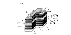
2,32 コア層
2a,2b クラッド層
32a 活性層
3,6,36 多層膜
4,34 選択酸化層
4a,34a 酸化部
5,35 コンタクト層
7,37,18 p側電極
8,38 n側電極
9,39 空孔
10 線欠陥部
11 n−InP基板
12,23,42 電源
14,16 クラッド層
15 活性層
17 コンタクト層
20 半導体レーザ
24 スイッチ
25 制御部
30 点欠陥部
まず、実施の形態1にかかるフォトニック結晶半導体デバイスである可変波長フィルタについて説明する。
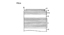
まず、MOCVD(Metal-Organic Chemical Vapor Deposition)結晶成長装置を用いて、n−InP半導体基板11上に下部DBR層1、コア層2、上部DBR層3、選択酸化層4、コンタクト層5を順次形成する。その後、フォトリソグラフィおよびドライエッチング装置によって、コンタクト層5および選択酸化層4の一部の領域21を除去する(図4)。
つぎに、この発明の第2の実施の形態について説明する。上述した実施の形態では、線欠陥部10を有したフォトニック結晶構造を有するフォトニック結晶半導体デバイスであったが、この実施の形態2では、点欠陥部を有したフォトニック結晶構造を有するフォトニック結晶半導体デバイスを実現している。
なお、図12における空孔39の深さは、図8に示した空孔9と同様に、下部DBR層1に到達しない深さにしてもよい。
図14は、本発明の第3の実施の形態を示すスーパープリズムとして使用されるフォトニクス結晶半導体デバイスを示す斜視図であり、また、図15は、図14に示すフォトニクス結晶半導体デバイスのコア層を示す平面図である。なお、これらの図において、図1、図11と同じ符合は同じ要素を示している。
図16は、本発明の第4の実施の形態に係る半導体レーザ集積型フォトニック結晶光デバイスを示す斜視断面図、図17は図16のI−I線断面図、図18は図16のII−II線断面図である。なお、図16、図17において、図1と同じ符合は同じ要素を示している。
ストライプ状の活性層15の一端は可変波長フィルタ40の線欠陥部10のコア層2の端部に接続されている。
Claims (9)
- 光の波長に近い2次元的な屈折率の周期構造に欠陥部を設けたフォトニック結晶構造を用いたフォトニック結晶半導体デバイスの製造方法において、
半導体基板上に下部半導体分布ブラッグ反射多層膜、前記フォトニック結晶が形成される半導体コア層、上部半導体分布ブラッグ反射多層膜、選択酸化層、コンタクト層を順次積層する積層工程と、
前記選択酸化層の一部に酸化した電流狭窄用の酸化部を形成する酸化処理工程と、
前記コンタクト層、前記選択酸化層、前記上部半導体分布ブラッグ反射多層膜および前記半導体コア層を貫通する複数の空孔を形成する空孔形成工程と、
前記上部半導体ブラッグ反射多層膜の上部に誘電体多層膜を形成する誘電体多層膜形成工程と、を有することを特徴とするフォトニック結晶半導体デバイスの製造方法。 - 前記空孔形成工程により、前記空孔に挟まれかつ空孔が存在しない線状の欠陥部を形成することを特徴とする請求項1に記載のフォトニック結晶半導体デバイスの製造方法。
- 前記空孔形成工程は、前記下部半導体分布ブラッグ反射多層膜の一部、あるいは前記下部半導体分布ブラッグ反射多層膜の全層を貫通する複数の空孔を形成することを含むことを特徴とする請求項1又は2に記載のフォトニック結晶半導体デバイスの製造方法。
- 前記コンタクト層の一部上面および前記半導体基板の下部に電極を形成する電極形成工程をさらに含むことを特徴とする請求項1〜3のいずれか一つに記載のフォトニック結晶半導体デバイスの製造方法。
- 前記半導体コア層は、活性層を有することを特徴とする請求項1〜4のいずれか一つに記載のフォトニック結晶半導体デバイスの製造方法。
- 前記半導体コア層は、多重量子井戸構造を有することを特徴とする請求項1〜5のいずれか一つに記載のフォトニック結晶半導体デバイスの製造方法。
- 前記半導体コア層は、InGaAsPを含むことを特徴とする請求項1〜6のいずれか一つに記載のフォトニック結晶半導体デバイスの製造方法。
- 前記半導体コア層は、GaInNAsSbを含むことを特徴とする請求項1〜6のいずれか一つに記載のフォトニック結晶半導体デバイスの製造方法。
- 前記半導体コア層は、AlGaInAsを含むことを特徴とする請求項1〜6のいずれか一つに記載のフォトニック結晶半導体デバイスの製造方法。
Priority Applications (1)
| Application Number | Priority Date | Filing Date | Title |
|---|---|---|---|
| JP2005518034A JP4833665B2 (ja) | 2004-02-17 | 2005-02-16 | フォトニック結晶半導体デバイスの製造方法 |
Applications Claiming Priority (4)
| Application Number | Priority Date | Filing Date | Title |
|---|---|---|---|
| JP2004040122 | 2004-02-17 | ||
| JP2004040122 | 2004-02-17 | ||
| PCT/JP2005/002342 WO2005078512A1 (ja) | 2004-02-17 | 2005-02-16 | フォトニック結晶半導体デバイスおよびその製造方法 |
| JP2005518034A JP4833665B2 (ja) | 2004-02-17 | 2005-02-16 | フォトニック結晶半導体デバイスの製造方法 |
Related Child Applications (1)
| Application Number | Title | Priority Date | Filing Date |
|---|---|---|---|
| JP2011034888A Division JP2011138156A (ja) | 2004-02-17 | 2011-02-21 | フォトニック結晶半導体デバイスおよびその製造方法 |
Publications (2)
| Publication Number | Publication Date |
|---|---|
| JPWO2005078512A1 JPWO2005078512A1 (ja) | 2008-01-17 |
| JP4833665B2 true JP4833665B2 (ja) | 2011-12-07 |
Family
ID=34857867
Family Applications (2)
| Application Number | Title | Priority Date | Filing Date |
|---|---|---|---|
| JP2005518034A Expired - Fee Related JP4833665B2 (ja) | 2004-02-17 | 2005-02-16 | フォトニック結晶半導体デバイスの製造方法 |
| JP2011034888A Pending JP2011138156A (ja) | 2004-02-17 | 2011-02-21 | フォトニック結晶半導体デバイスおよびその製造方法 |
Family Applications After (1)
| Application Number | Title | Priority Date | Filing Date |
|---|---|---|---|
| JP2011034888A Pending JP2011138156A (ja) | 2004-02-17 | 2011-02-21 | フォトニック結晶半導体デバイスおよびその製造方法 |
Country Status (4)
| Country | Link |
|---|---|
| US (1) | US7525726B2 (ja) |
| EP (1) | EP1722265A4 (ja) |
| JP (2) | JP4833665B2 (ja) |
| WO (1) | WO2005078512A1 (ja) |
Families Citing this family (25)
| Publication number | Priority date | Publication date | Assignee | Title |
|---|---|---|---|---|
| JP5008874B2 (ja) * | 2005-02-23 | 2012-08-22 | 住友電気工業株式会社 | 受光素子と受光素子を用いた光通信用受信モジュールおよび受光素子を用いた計測器 |
| US7412144B2 (en) * | 2005-07-22 | 2008-08-12 | The United States Of America As Represented By The Secretary Of The Army | Photonic crystal-based optical waveguide modulator |
| JP2007147934A (ja) * | 2005-11-28 | 2007-06-14 | Rohm Co Ltd | 光制御装置およびそれを用いた光制御システム |
| JP2007173353A (ja) * | 2005-12-20 | 2007-07-05 | Kyoto Univ | フォトニック結晶発光ダイオード及びその製造方法 |
| WO2008055409A1 (en) * | 2006-11-09 | 2008-05-15 | Yiquan Li | A vertical surface light emitting device with multiple active layers |
| JP2009170508A (ja) * | 2008-01-11 | 2009-07-30 | Furukawa Electric Co Ltd:The | 面発光半導体レーザ及びその製造方法 |
| JP5188259B2 (ja) * | 2008-05-02 | 2013-04-24 | キヤノン株式会社 | 3次元フォトニック結晶を用いた発光素子 |
| KR101799521B1 (ko) * | 2011-05-24 | 2017-11-20 | 삼성전자 주식회사 | 광결정형 광변조기 및 이를 구비하는 3차원 영상 획득 장치 |
| CN204258035U (zh) | 2012-05-31 | 2015-04-08 | 古河电气工业株式会社 | 半导体激光器模块 |
| US9042418B2 (en) * | 2013-02-11 | 2015-05-26 | California Institute Of Technology | III-V photonic crystal microlaser bonded on silicon-on-insulator |
| EP3521920B1 (en) * | 2016-09-29 | 2021-09-29 | Panasonic Intellectual Property Management Co., Ltd. | Optical scan device, light receiving device, and optical detection system |
| DE102016014938B4 (de) * | 2016-12-14 | 2019-06-27 | Forschungsverbund Berlin E.V. | Lichtemittervorrichtung, basierend auf einem photonischen Kristall mit säulen- oder wandförmigen Halbleiterelementen, und Verfahren zu deren Betrieb und Herstellung |
| JP7090861B2 (ja) * | 2017-02-28 | 2022-06-27 | 学校法人上智学院 | 光デバイスおよび光デバイスの製造方法 |
| JP7333666B2 (ja) * | 2017-02-28 | 2023-08-25 | 学校法人上智学院 | 光デバイスおよび光デバイスの製造方法 |
| SG11202005786SA (en) * | 2018-01-18 | 2020-08-28 | Iqe Plc | Porous distributed bragg reflectors for laser applications |
| DE102020200468A1 (de) * | 2020-01-16 | 2021-07-22 | OSRAM Opto Semiconductors Gesellschaft mit beschränkter Haftung | Halbleiterlaserdiode und verfahren zur herstellung einer halbleiterlaserdiode |
| CN111916999B (zh) * | 2020-07-13 | 2022-04-19 | 清华大学 | 具有槽结构的分布式反馈激光器及制备方法 |
| CN111916998A (zh) * | 2020-07-13 | 2020-11-10 | 清华大学 | 基于w3光子晶体缺陷波导的分布式反馈激光器及制备方法 |
| CN111917000A (zh) * | 2020-07-13 | 2020-11-10 | 清华大学 | 具有微腔结构的分布式反馈激光器及制备方法 |
| CN111916997B (zh) * | 2020-07-13 | 2023-11-28 | 清华大学 | 基于空气孔的分布式反馈激光器及制备方法 |
| JP7485284B2 (ja) * | 2020-07-14 | 2024-05-16 | 国立大学法人京都大学 | フォトニック結晶面発光レーザ素子 |
| GB2612040B (en) | 2021-10-19 | 2025-02-12 | Iqe Plc | Porous distributed Bragg reflector apparatuses, systems, and methods |
| JP2023066877A (ja) * | 2021-10-29 | 2023-05-16 | ローム株式会社 | 光センサ及び光センサに備わるバンドパスフィルタ |
| JP7546120B1 (ja) * | 2023-07-31 | 2024-09-05 | Nttイノベーティブデバイス株式会社 | 平面光波回路 |
| CN118981065B (zh) * | 2024-08-06 | 2025-10-03 | 中国计量大学 | 一种基于一维缺陷光子晶体堆叠的太赫兹吸收谱器件及其制备方法 |
Citations (4)
| Publication number | Priority date | Publication date | Assignee | Title |
|---|---|---|---|---|
| JPH0750443A (ja) * | 1993-08-04 | 1995-02-21 | Hitachi Ltd | 半導体光集積素子及びその製造方法 |
| JPH10284806A (ja) * | 1997-04-10 | 1998-10-23 | Canon Inc | フォトニックバンド構造を有する垂直共振器レーザ |
| GB2366666A (en) * | 2000-09-11 | 2002-03-13 | Toshiba Res Europ Ltd | Optical device |
| JP2002303836A (ja) * | 2001-04-04 | 2002-10-18 | Nec Corp | フォトニック結晶構造を有する光スイッチ |
Family Cites Families (19)
| Publication number | Priority date | Publication date | Assignee | Title |
|---|---|---|---|---|
| FR2734097B1 (fr) * | 1995-05-12 | 1997-06-06 | Thomson Csf | Laser a semiconducteurs |
| US6134043A (en) | 1998-08-11 | 2000-10-17 | Massachusetts Institute Of Technology | Composite photonic crystals |
| US6468823B1 (en) * | 1999-09-30 | 2002-10-22 | California Institute Of Technology | Fabrication of optical devices based on two dimensional photonic crystal structures and apparatus made thereby |
| US6499888B1 (en) * | 1999-12-20 | 2002-12-31 | Corning Lasertron, Inc. | Wide ridge pump laser |
| JP2001257425A (ja) * | 2000-03-13 | 2001-09-21 | Matsushita Electric Ind Co Ltd | 半導体レーザ素子及びその製造方法 |
| JP2002064244A (ja) * | 2000-06-06 | 2002-02-28 | Furukawa Electric Co Ltd:The | 分布帰還型半導体レーザ素子 |
| US6674949B2 (en) * | 2000-08-15 | 2004-01-06 | Corning Incorporated | Active photonic crystal waveguide device and method |
| DK1371120T3 (da) * | 2001-03-09 | 2013-07-22 | Alight Photonics Aps | Bølgetypekontrol ved anvendelse af transversal båndgabsstruktur i vcsels |
| US6574383B1 (en) * | 2001-04-30 | 2003-06-03 | Massachusetts Institute Of Technology | Input light coupler using a pattern of dielectric contrast distributed in at least two dimensions |
| US6560006B2 (en) * | 2001-04-30 | 2003-05-06 | Agilent Technologies, Inc. | Two-dimensional photonic crystal slab waveguide |
| JP2003131028A (ja) * | 2001-08-14 | 2003-05-08 | Autocloning Technology:Kk | 光回路 |
| JP3729134B2 (ja) | 2002-01-29 | 2005-12-21 | 松下電器産業株式会社 | 光ピックアップ用2波長半導体レーザ光源 |
| US6829281B2 (en) * | 2002-06-19 | 2004-12-07 | Finisar Corporation | Vertical cavity surface emitting laser using photonic crystals |
| JP2004037938A (ja) * | 2002-07-04 | 2004-02-05 | Furukawa Electric Co Ltd:The | 光素子 |
| JP4569942B2 (ja) * | 2002-09-26 | 2010-10-27 | 三菱電機株式会社 | 光アクティブデバイス |
| US6943377B2 (en) * | 2002-11-21 | 2005-09-13 | Sensor Electronic Technology, Inc. | Light emitting heterostructure |
| US7136561B2 (en) * | 2003-03-26 | 2006-11-14 | Tdk Corporation | Two-dimensional photonic crystal, and waveguide and resonator using the same |
| US7250635B2 (en) * | 2004-02-06 | 2007-07-31 | Dicon Fiberoptics, Inc. | Light emitting system with high extraction efficency |
| JP2005274927A (ja) * | 2004-03-24 | 2005-10-06 | Furukawa Electric Co Ltd:The | フォトニック結晶デバイス |
-
2005
- 2005-02-16 EP EP05719194A patent/EP1722265A4/en not_active Withdrawn
- 2005-02-16 WO PCT/JP2005/002342 patent/WO2005078512A1/ja not_active Ceased
- 2005-02-16 JP JP2005518034A patent/JP4833665B2/ja not_active Expired - Fee Related
-
2006
- 2006-08-17 US US11/505,428 patent/US7525726B2/en not_active Expired - Fee Related
-
2011
- 2011-02-21 JP JP2011034888A patent/JP2011138156A/ja active Pending
Patent Citations (4)
| Publication number | Priority date | Publication date | Assignee | Title |
|---|---|---|---|---|
| JPH0750443A (ja) * | 1993-08-04 | 1995-02-21 | Hitachi Ltd | 半導体光集積素子及びその製造方法 |
| JPH10284806A (ja) * | 1997-04-10 | 1998-10-23 | Canon Inc | フォトニックバンド構造を有する垂直共振器レーザ |
| GB2366666A (en) * | 2000-09-11 | 2002-03-13 | Toshiba Res Europ Ltd | Optical device |
| JP2002303836A (ja) * | 2001-04-04 | 2002-10-18 | Nec Corp | フォトニック結晶構造を有する光スイッチ |
Also Published As
| Publication number | Publication date |
|---|---|
| US20070013991A1 (en) | 2007-01-18 |
| EP1722265A1 (en) | 2006-11-15 |
| EP1722265A4 (en) | 2008-07-02 |
| JP2011138156A (ja) | 2011-07-14 |
| EP1722265A8 (en) | 2007-03-21 |
| US7525726B2 (en) | 2009-04-28 |
| WO2005078512A1 (ja) | 2005-08-25 |
| JPWO2005078512A1 (ja) | 2008-01-17 |
Similar Documents
| Publication | Publication Date | Title |
|---|---|---|
| JP4833665B2 (ja) | フォトニック結晶半導体デバイスの製造方法 | |
| US7697586B2 (en) | Surface-emitting laser | |
| KR100759603B1 (ko) | 수직 공진기형 면발광 레이저 장치 | |
| JP4569942B2 (ja) | 光アクティブデバイス | |
| US20070201527A1 (en) | Vertical cavity surface emitting laser | |
| JP4761426B2 (ja) | 光デバイスおよび半導体レーザ発振器 | |
| JP4954992B2 (ja) | 半導体光反射素子及び該半導体光反射素子を用いる半導体レーザ及び該半導体レーザを用いる光トランスポンダ | |
| KR102368946B1 (ko) | 파장 가변 레이저 장치 및 이를 제조하는 방법 | |
| JP2005538532A (ja) | 傾斜型共振器半導体レーザー(tcsl)及びその製造方法 | |
| US20080107145A1 (en) | Structure having photonic crystal and surface-emitting laser using the same | |
| KR20110126661A (ko) | 하이브리드 수직공진 레이저 | |
| KR20140059762A (ko) | 반사율이 조절된 격자 미러 | |
| JP2010140967A (ja) | 光モジュール | |
| JPWO2009116152A1 (ja) | 光素子及びその製造方法 | |
| JP2008218975A (ja) | 構造体、面発光レーザ、及び面発光レーザを備えた発光装置 | |
| JP2015175902A (ja) | 光導波路、スポットサイズ変換器、偏光フィルタ、光結合器、光検出器、光合分波器、および、レーザ素子 | |
| JP5979897B2 (ja) | スーパールミネッセントダイオード、スーパールミネッセントダイオードを備えたsd−octシステム | |
| US10243330B2 (en) | Optoelectronic device with resonant suppression of high order optical modes and method of making same | |
| JP4103558B2 (ja) | 面発光レーザ | |
| JP2008098379A (ja) | 2次元フォトニック結晶面発光レーザおよびその製造方法 | |
| KR101466703B1 (ko) | 광대역 파장조절 표면방출 레이저 | |
| JP2024547119A (ja) | 分布帰還型レーザおよびそのようなレーザを製造する方法 | |
| JP4982838B2 (ja) | 光制御素子 | |
| JP2010045066A (ja) | 半導体レーザ装置 | |
| JP2017139341A (ja) | 光素子、集積型光素子および光素子モジュール |
Legal Events
| Date | Code | Title | Description |
|---|---|---|---|
| A621 | Written request for application examination |
Free format text: JAPANESE INTERMEDIATE CODE: A621 Effective date: 20080201 |
|
| RD03 | Notification of appointment of power of attorney |
Free format text: JAPANESE INTERMEDIATE CODE: A7423 Effective date: 20081027 |
|
| RD04 | Notification of resignation of power of attorney |
Free format text: JAPANESE INTERMEDIATE CODE: A7424 Effective date: 20100818 |
|
| RD02 | Notification of acceptance of power of attorney |
Free format text: JAPANESE INTERMEDIATE CODE: A7422 Effective date: 20100909 |
|
| RD04 | Notification of resignation of power of attorney |
Free format text: JAPANESE INTERMEDIATE CODE: A7424 Effective date: 20100909 |
|
| A131 | Notification of reasons for refusal |
Free format text: JAPANESE INTERMEDIATE CODE: A131 Effective date: 20100915 |
|
| RD03 | Notification of appointment of power of attorney |
Free format text: JAPANESE INTERMEDIATE CODE: A7423 Effective date: 20100921 |
|
| RD03 | Notification of appointment of power of attorney |
Free format text: JAPANESE INTERMEDIATE CODE: A7423 Effective date: 20101005 |
|
| A521 | Request for written amendment filed |
Free format text: JAPANESE INTERMEDIATE CODE: A821 Effective date: 20101005 |
|
| AA92 | Notification that decision to refuse application was cancelled |
Free format text: JAPANESE INTERMEDIATE CODE: A971092 Effective date: 20101130 |
|
| A131 | Notification of reasons for refusal |
Free format text: JAPANESE INTERMEDIATE CODE: A131 Effective date: 20101221 |
|
| RD04 | Notification of resignation of power of attorney |
Free format text: JAPANESE INTERMEDIATE CODE: A7424 Effective date: 20101228 |
|
| RD03 | Notification of appointment of power of attorney |
Free format text: JAPANESE INTERMEDIATE CODE: A7423 Effective date: 20110217 |
|
| A521 | Request for written amendment filed |
Free format text: JAPANESE INTERMEDIATE CODE: A523 Effective date: 20110221 |
|
| RD04 | Notification of resignation of power of attorney |
Free format text: JAPANESE INTERMEDIATE CODE: A7424 Effective date: 20110815 |
|
| TRDD | Decision of grant or rejection written | ||
| A01 | Written decision to grant a patent or to grant a registration (utility model) |
Free format text: JAPANESE INTERMEDIATE CODE: A01 Effective date: 20110906 |
|
| A01 | Written decision to grant a patent or to grant a registration (utility model) |
Free format text: JAPANESE INTERMEDIATE CODE: A01 |
|
| A61 | First payment of annual fees (during grant procedure) |
Free format text: JAPANESE INTERMEDIATE CODE: A61 Effective date: 20110922 |
|
| FPAY | Renewal fee payment (event date is renewal date of database) |
Free format text: PAYMENT UNTIL: 20140930 Year of fee payment: 3 |
|
| LAPS | Cancellation because of no payment of annual fees |