JP4834883B2 - Substrate processing equipment - Google Patents
Substrate processing equipment Download PDFInfo
- Publication number
- JP4834883B2 JP4834883B2 JP2008005913A JP2008005913A JP4834883B2 JP 4834883 B2 JP4834883 B2 JP 4834883B2 JP 2008005913 A JP2008005913 A JP 2008005913A JP 2008005913 A JP2008005913 A JP 2008005913A JP 4834883 B2 JP4834883 B2 JP 4834883B2
- Authority
- JP
- Japan
- Prior art keywords
- substrate
- gas
- process chamber
- space
- plasma
- Prior art date
- Legal status (The legal status is an assumption and is not a legal conclusion. Google has not performed a legal analysis and makes no representation as to the accuracy of the status listed.)
- Expired - Fee Related
Links
- 239000000758 substrate Substances 0.000 title claims description 161
- 238000000034 method Methods 0.000 claims description 152
- 238000005192 partition Methods 0.000 claims description 63
- 238000002347 injection Methods 0.000 claims description 31
- 239000007924 injection Substances 0.000 claims description 31
- 238000004380 ashing Methods 0.000 claims description 16
- 238000000638 solvent extraction Methods 0.000 claims description 2
- 239000007789 gas Substances 0.000 description 100
- 239000004065 semiconductor Substances 0.000 description 5
- 230000006837 decompression Effects 0.000 description 4
- 238000012986 modification Methods 0.000 description 3
- 230000004048 modification Effects 0.000 description 3
- 239000004973 liquid crystal related substance Substances 0.000 description 2
- 238000004519 manufacturing process Methods 0.000 description 2
- 239000012495 reaction gas Substances 0.000 description 2
- 239000006227 byproduct Substances 0.000 description 1
- 239000003795 chemical substances by application Substances 0.000 description 1
- 238000010586 diagram Methods 0.000 description 1
- 238000007599 discharging Methods 0.000 description 1
- 239000010419 fine particle Substances 0.000 description 1
- 238000010438 heat treatment Methods 0.000 description 1
- 238000009434 installation Methods 0.000 description 1
- 239000012212 insulator Substances 0.000 description 1
- 239000000463 material Substances 0.000 description 1
- 238000000206 photolithography Methods 0.000 description 1
- 229920002120 photoresistant polymer Polymers 0.000 description 1
- 238000000926 separation method Methods 0.000 description 1
Images




Classifications
-
- A—HUMAN NECESSITIES
- A47—FURNITURE; DOMESTIC ARTICLES OR APPLIANCES; COFFEE MILLS; SPICE MILLS; SUCTION CLEANERS IN GENERAL
- A47L—DOMESTIC WASHING OR CLEANING; SUCTION CLEANERS IN GENERAL
- A47L17/00—Apparatus or implements used in manual washing or cleaning of crockery, table-ware, cooking-ware or the like
- A47L17/04—Pan or pot cleaning utensils
- A47L17/08—Pads; Balls of steel wool, wire, or plastic meshes
-
- D—TEXTILES; PAPER
- D06—TREATMENT OF TEXTILES OR THE LIKE; LAUNDERING; FLEXIBLE MATERIALS NOT OTHERWISE PROVIDED FOR
- D06M—TREATMENT, NOT PROVIDED FOR ELSEWHERE IN CLASS D06, OF FIBRES, THREADS, YARNS, FABRICS, FEATHERS OR FIBROUS GOODS MADE FROM SUCH MATERIALS
- D06M15/00—Treating fibres, threads, yarns, fabrics, or fibrous goods made from such materials, with macromolecular compounds; Such treatment combined with mechanical treatment
- D06M15/19—Treating fibres, threads, yarns, fabrics, or fibrous goods made from such materials, with macromolecular compounds; Such treatment combined with mechanical treatment with synthetic macromolecular compounds
- D06M15/37—Macromolecular compounds obtained otherwise than by reactions only involving carbon-to-carbon unsaturated bonds
- D06M15/564—Polyureas, polyurethanes or other polymers having ureide or urethane links; Precondensation products forming them
Landscapes
- Chemical & Material Sciences (AREA)
- Chemical Kinetics & Catalysis (AREA)
- Engineering & Computer Science (AREA)
- Textile Engineering (AREA)
- Drying Of Semiconductors (AREA)
Description
本発明は、基板処理装置に関し、特に、基板が工程チャンバーでローディング/アンローディングされるとき、開き、閉められる基板出入口を有する基板処理装置及び方法に関する。 The present invention relates to a substrate processing apparatus, and more particularly, to a substrate processing apparatus and method having a substrate entrance that is opened and closed when the substrate is loaded / unloaded in a process chamber.
通常に、半導体ウエハまたは液晶基板を処理するための装置において、半導体ウエハまたは液晶基板は、工程チャンバーに備わる基板移送通路である基板出入口を通して出し入れされるが、このような基板出入口には、この通路を開閉するゲートバルブが備わる。 Usually, in an apparatus for processing a semiconductor wafer or a liquid crystal substrate, the semiconductor wafer or the liquid crystal substrate is taken in and out through a substrate inlet / outlet which is a substrate transfer passage provided in a process chamber. It has a gate valve that opens and closes.
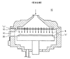
図1に示すように、ゲートバルブ20は、工程チャンバー10の一側壁13に設けられて、工程チャンバー10の基板移送通路である基板出入口12を開閉する。前記のような構造で、基板Wは、工程チャンバー10一側面に形成された基板出入口12を通して工程チャンバー10内に搬入または搬出される。
As shown in FIG. 1, the
以上のような従来の工程チャンバーでは、次のような問題点が発生する。 In the conventional process chamber as described above, the following problems occur.
従来のゲートバルブ20は、工程チャンバー10外部に結合されて選択的に工程チャンバー10の一側面に形成された基板出入口12を開閉するので、工程チャンバー10内部の空間的な非対称が発生して、基板Wに対するプラズマ処理などを行う場合、不均一が発生する。即ち、工程チャンバー10、一側面13に形成された基板出入口12によってチャンバー隔壁の厚さほどの空間的な不均一が発生し、これに従って工程チャンバー10内部でプラズマ処理などを行う場合に均一な処理が難しくなる問題点が発生する。特に、基板の左右エッジ部分(a部分とb部分)でプラズマ密度差が存在し、これによって基板処理の均一度が低くなる。
Since the
一方、このような問題を改善させるために、ドア内側だけスリットを共に作動してこのような問題を防ぐ方法も使用する。しかしながら、この方法では、エラーを引き起こしたり微粒子の発生を招く可動部材を工程チャンバーに設ける必要がある。 On the other hand, in order to improve such a problem, a method of preventing such a problem by operating the slits only inside the door is also used. However, in this method, it is necessary to provide a movable member in the process chamber that causes an error or causes generation of fine particles.
本発明の目的は、工程チャンバー内部空間の空間的な不均衡によるプラズマ及びガスの密度差を最低化できる基板処理装置及び方法を提供することにある。 An object of the present invention is to provide a substrate processing apparatus and method capable of minimizing a plasma and gas density difference due to a spatial imbalance in a process chamber internal space.
本発明の目的は、工程チャンバー内部でプラズマ処理などを行う場合に均一なプラズマ密度を提供して均一な基板処理が可能な基板処理装置及び方法を提供することにある。 An object of the present invention is to provide a substrate processing apparatus and method capable of providing a uniform plasma density and performing uniform substrate processing when performing plasma processing or the like inside a process chamber.
前記の目的を達成するための本発明の特徴によれば、基板処理装置は、基板処理工程が行われたプロセス空間を提供し、かつ一側面に基板の入出のための基板出入口が設けられており、内部に排気口が設けられており、前記基板出入口を開閉するゲートバルブを有する工程チャンバーと、前記工程チャンバー内部の底部に設けられ、前記基板出入口を通して入ってきた基板が置かれる基板支持部材と、前記工程チャンバーの上側に設けられており、かつ、前記プロセス空間でプラズマ及び工程ガスを分配するための多数のガス噴射流路を有するガス分配プレートとを含む。
そして、前記前記基板出入口と隣接した領域に形成されたガス噴射流路の直径の大きさは、前記基板出入口と隣接した領域以外に形成されたガス噴射流路の直径の大きさよりも大きい。
According to a feature of the present invention for achieving the above object, the substrate processing apparatus provides a process space in which a substrate processing step is performed, and a substrate entrance for entering and exiting the substrate is provided on one side surface. A process chamber having a gate valve that opens and closes the substrate entrance and exit, and a substrate support member that is provided at the bottom of the process chamber and on which the substrate that has entered through the substrate entrance is placed. And a gas distribution plate provided on the upper side of the process chamber and having a plurality of gas injection channels for distributing plasma and process gas in the process space.
The diameter of the gas injection channel formed in the region adjacent to the substrate inlet / outlet is larger than the diameter of the gas injection channel formed in a region other than the region adjacent to the substrate inlet / outlet.
本発明の一実施形態によれば、前記基板処理装置は、前記ガス分配プレートの上側にプラズマ生成のためのプラズマ源をさらに含む。 According to an embodiment of the present invention, the substrate processing apparatus further includes a plasma source for generating plasma on the gas distribution plate.
本発明の一実施形態によれば、前記基板出入口と隣接した領域に形成されたガス噴射流路の大きさは、他の領域に形成されたガス噴射流路の大きさより1%から1000%大きい。 According to an embodiment of the present invention, the size of the gas injection flow path formed in the region adjacent to the substrate inlet / outlet is 1% to 1000% larger than the size of the gas injection flow channel formed in the other region. .
前記の目的を達成するための本発明の特徴によれば、基板上にアッシング工程を行う装置において、内部に基板処理工程が行われるプロセス空間を提供し、かつ一側面に基板の入出のための基板出入口を有する工程チャンバーと、前記工程チャンバー内部に設けられて、工程時基板を支持する複数の基板支持部材と、前記基板支持部材各々に電力を印加する電力印加機と、プラズマを発生させて、前記工程チャンバー内部でプラズマを供給するプラズマ生成部材と、前記工程チャンバー内のガスを排気させる排気部材と、前記基板支持部材が設けられる前記工程チャンバー内のプロセス空間及び前記排気部材の排気空間を区画する区画部材と、前記工程チャンバー内のプロセス空間上部に設けられて、前記基板支持部材各々に置かれた基板側でプラズマ及び工程ガスを分配するためのガス分配プレートとを含む。ガス分配プレートは、基板出入口と隣接した領域を有している。基板出入口と隣接した領域に形成されたガス噴射流路の直径は、基板出入口と隣接した領域以外の領域に形成されたガス噴射流路の直径よりも大きい。 According to a feature of the present invention for achieving the above object, in an apparatus for performing an ashing process on a substrate, a process space in which the substrate processing process is performed is provided, and a substrate is placed on one side for entering and exiting. A process chamber having a substrate inlet / outlet; a plurality of substrate support members provided inside the process chamber for supporting the substrate during the process; a power application device for applying power to each of the substrate support members; and generating plasma. A plasma generating member that supplies plasma inside the process chamber, an exhaust member that exhausts gas in the process chamber, a process space in the process chamber in which the substrate support member is provided, and an exhaust space of the exhaust member A partition member to be partitioned, and a substrate side provided on each of the substrate support members, which is provided above the process space in the process chamber And a gas distribution plate for distributing plasma and process gases. The gas distribution plate has a region adjacent to the substrate inlet / outlet. The diameter of the gas injection channel formed in the region adjacent to the substrate inlet / outlet is larger than the diameter of the gas injection channel formed in the region other than the region adjacent to the substrate inlet / outlet.
本発明の一実施形態によれば、前記ガス分配プレートは、前記排気部材と隣接した領域に形成されたガス噴射流路の大きさが他の領域に形成されたガス噴射流路の大きさより大きい。 According to an embodiment of the present invention, in the gas distribution plate, the size of the gas injection channel formed in the region adjacent to the exhaust member is larger than the size of the gas injection channel formed in the other region. .
本発明の一実施形態によれば、前記排気部材は、前記工程チャンバーの下部壁で前記基板支持部材各々の中心を基準として環状で形成される排気口を通して前記プロセス空間内のガスを排出させる共通排気管を含み、前記区画部材は、前記工程チャンバー内部で前記プロセス空間を区画する区画壁と、前記プロセス空間各々から排気されるガスが独立的に排気されるように前記共通排気管内の排気空間を区画する隔壁とを含む。 According to an embodiment of the present invention, the exhaust member discharges the gas in the process space through an exhaust port formed in an annular shape with respect to the center of each of the substrate support members on the lower wall of the process chamber. The partition member includes an exhaust pipe, and the partition member partitions the process space inside the process chamber, and an exhaust space in the common exhaust pipe so that gas exhausted from each of the process spaces is independently exhausted. And partition walls.
本発明の一実施形態によれば 前記区画壁は、前記支持部材の中心を通して前記区画壁と平行する線を中心で左右対称になるように前記工程空間を区画し、前記隔壁は、前記隔壁を中心で左右対称になるように前記排気空間を区画する。 According to an embodiment of the present invention, the partition wall partitions the process space so as to be symmetrical about a line parallel to the partition wall through the center of the support member, and the partition wall includes the partition wall. The exhaust space is partitioned so as to be symmetrical at the center.
本発明によれば、工程チャンバー内部空間の空間的な不均衡によるプラズマ及びガスの分布差を最低化できる。本発明は、工程チャンバー内部でプラズマ処理などを行う場合に均一なプラズマ密度を提供して均一な基板処理が可能である。 According to the present invention, the difference in plasma and gas distribution due to the spatial imbalance of the process chamber internal space can be minimized. The present invention provides a uniform plasma density when performing plasma processing or the like inside a process chamber, and enables uniform substrate processing.
以下、本発明によるアッシング装置を添付した図面を参照して、詳細に説明する。 Hereinafter, an ashing device according to the present invention will be described in detail with reference to the accompanying drawings.
本発明は、ここで説明される一実施形態に限定されず、他の形態で具現されることができる。ここで紹介される一実施形態は開示された内容が徹底かつ完全になるように、また当業者に本発明の思想と特徴が十分に伝達できるようにするために提供されるものである。図面において、各々の装置は、本発明の明確性を期するために概略的に示されたものである。また、各々の装置には本明細書で詳細に説明されない各種の多様な付加装置が備わっている場合がある。明細書全体にわたって、同一な図面符号は同一な構成要素を表す。 The present invention is not limited to one embodiment described herein, and may be embodied in other forms. Rather, these embodiments are provided so that this disclosure will be thorough and complete, and will fully convey the spirit and characteristics of the invention to those skilled in the art. In the drawings, each device is schematically illustrated for clarity of the invention. In addition, each device may include various various additional devices not described in detail in this specification. Throughout the specification, the same reference numerals represent the same components.
(一実施形態)
本実施形態において、プラズマを用いてフォトリソグラフィー工程の後、基板上に残っている不要な感光剤を除去するプラズマアッシング装置を挙げて説明する。しかしながら、本発明の技術的思想は、これに限定されず、プラズマを用いて半導体基板を処理する他の種類の全ての装置にも適用されることができる。
(One embodiment)
In this embodiment, a plasma ashing apparatus that removes unnecessary photosensitive agent remaining on a substrate after a photolithography process using plasma will be described. However, the technical idea of the present invention is not limited to this, and can be applied to all other types of apparatuses that process a semiconductor substrate using plasma.
また、本実施形態においては、プラズマを生成させるためのエネルギー源で、マイクロ波を挙げて説明するが、その他にも高周波電源など多様なエネルギー源が使用されることができる。 In the present embodiment, the microwave is used as an energy source for generating plasma, but various other energy sources such as a high-frequency power source can be used.
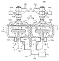
図2〜図6に示すように、本発明の一実施形態による基板処理装置100は、プラズマ源で生成されるラジカル(radical)を用いて半導体素子製造用基板(以下、基板と称する)の表面をアッシングするための半導体製造装置である。
As shown in FIGS. 2 to 6, a
図2〜図4に示すように、基板処理装置100は、所定の密閉された雰囲気を提供する工程チャンバー110、基板支持部材120、排気部材150、区画部材160、プラズマ生成部材140、そして第1、2ガス分配プレート170a、170bを有するガス供給部材130を含む。
As shown in FIGS. 2 to 4, the
工程チャンバー110は、内部にアッシング工程(ashing process)を行うプロセス空間を提供する。工程チャンバー110は、二つの基板を同時に処理できる構造を有する。即ち、工程チャンバー110のプロセス空間は、第1空間aと第2空間bで区画される。第1空間aと第2空間bの各々は、工程の時受容された一枚の基板上にアッシング工程が行われる空間である。工程チャンバー110の一側壁には、第1空間aと第2空間bで各々基板出入がなされる基板出入口112が形成される。基板出入口112は、ゲートバルブのような開閉ドア114により開閉される。
The
そして、工程チャンバー110の下部壁には、工程チャンバー110内ガスが排気される排気口116が提供される。排気口116は、各々の基板支持部材120を中心で環状で形成される。本一実施形態においては、二つの空間を有する工程チャンバー110を挙げて説明しているが、工程チャンバー110内区画空間は三つ以上でもよい。
The lower wall of the
前記工程チャンバー110の第1空間aと第2空間bには、工程の時、基板を支持する基板支持部材120が各々設けられる。基板支持部材120としては、静電チャックが使用されることができる。また、基板支持部材120は,工程の時、基板Wを固着させて予め設定された工程温度で加熱する。このために、基板支持部材120は、基板を一定温度で加熱するためのヒーター及び前記ロボットによって基板の移送が容易に基板を支持する形態で昇下降駆動するリフトアセンブリー(図示せず)などが備わった通常の構成を有する。基板支持部材120は、基板W上のフォトレジスターが除去できる適正温度200-400℃で維持される。図示されていないが、通常のリフトアセンブリーは、基板出入口112の開放によってロボット(図示せず)によって投入位置になる基板Wの底面を支えて支持するリフトピンと、リフトピンを上昇(アップ位置)/下降(ダウン位置)させるための駆動部を含むことができる。基板Wは、リフトピンによって基板支持部材上面から離隔されたアップ位置と、基板支持部材上面に置かれるダウン位置で移動される。そして、基板支持部材120には、電力印加機122が連結される。電力印加機122は、基板支持部材120に予め設定されたバイアス電力を印加する。
The first space a and the second space b of the
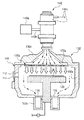
図3に示すように、排気部材150は、工程チャンバー110の内部を真空状態で形成し、アッシング工程が行われる間に発生する反応副産物などを排出させるためのものである。
As shown in FIG. 3, the
排気部材150は、共通排気管152、メーン排気管154、そして減圧部材156を含む。共通排気管152は、工程チャンバー110内部ガスを外部で排気させる。共通排気管152は、第1及び第2空間a、b内のガスを全て排気するように工程チャンバー110の排気口116と連結される。ここで、より効果的な分離排気のために排気部材150は、単一排気管152aをさらに備えることができる。単一排気管152aは、排気口116から下方向で環状に延びる。単一排気管152aは、工程時第1及び第2空間a、bから排気口116を通して排気されるガスが均一な流れを有し、共通排気管152へ移動されるようにする。単一排気管152aは、排気口116を通して排気されるガスの逆流及び流れの不均一を防止する。共通排気管152は、単一排気管152aの間で単一各々の第1及び第2空間a、bと連結される排気管152aから排気されるガスを排気させる。メーン排気管154は、共通排気管152と連結される。減圧部材156は、メーン排気管154に設けられる。減圧部材156は、工程チャンバー110内部圧力を減圧するように第1及び第2空間a、b内のガスを強制に吸入する。減圧部材156としては、真空ポンプが使用されることができる。
The
区画部材160は、区画壁162及び隔壁164を含む。区画壁162は、第1空間a及び第2空間bが同等な構造を有するように工程チャンバー110内部を区画する。区画壁162は、工程チャンバー110内部中央で上下に垂直に設けられる。この際、区画壁162は、第1空間a及び第2空間b各々が線X2、X3を基準として左右対称になるように工程チャンバー110内部を区画する。線X2は、第1空間aの基板支持部材120中心を横切る仮想線で、線X3は、第2空間の基板支持部材120の中心を横切る仮想線である。この際、線X2、X3は、区画壁162を垂直に横切る線X1と平行する。区画壁162の外側面162aは、線X2、X3を基準として工程チャンバー110の内側面111と対称される形状で製作される。
The
隔壁164は、第1空間a及び第2空間bから排気されるガスが分離排気されるように共通排気管152内部の排気空間を区画する。隔壁164は、区画壁162から下方向に垂直に延びる。隔壁164は、共通排気管152とメーン排気管154が連結される部分まで延びることが好ましい。隔壁164は、第1空間a内ガスが排気される第1排気空間cと第2空間b内ガスが排気される第2排気空間dが互いに同等な構造を有するように共通排気管152を区画する。
The
区画部材160は、第1空間a及び第2空間bの分離排気のために提供される。また、区画部材160は、第1空間aの基板支持部材120に印加される電力と第2空間bの基板支持部材120に印加される電力が互いに影響を受けないように第1空間a及び第2空間bを区画する。従って、区画部材160の材質は、絶縁体であることが好ましい。
The
本一実施形態においては、区画部材160が一体型の区画壁162及び隔壁164を備えて工程チャンバー110及び共通排気管152を区画することを挙げて説明しているが、区画部材の構造及び形状、そして設置方式は、多様に変更及び変形できる。例えば、区画部材160は、区画壁162と隔壁164が互い分離可能な構造からなることができ、区画壁162と隔壁164は、複数個からなることができる。又は、区画部材160の区画壁162は、工程チャンバー110に固定設けられ、隔壁166は、共通排気管152に固定設けられて基板処理装置100を組み立てる際、区画壁と隔壁が互いに締結される構成である場合もある。
In the present embodiment, the
プラズマ生成部材140は、工程の時、プラズマを発生させて工程チャンバー110で供給する。プラズマ生成部材140としては、遠隔プラズマ発生装置が使用される。プラズマ生成部材140は、第1生成部材142及び第2生成部材144を含む。第1生成部材142は、工程の時、第1供給部材132でプラズマを供給し、第2生成部材144は、工程の時、第2供給部材134でプラズマを供給する。第1及び第2生成部材142、144各々は、マグネトロン142a、144a、導波管142b、144b、そしてガス供給管142c、144cを含む。マグネトロン142a、144aは、工程の時、プラズマ生成のためのマイクロ波を発生させる。導波管142bは、マグネトロン142aで生成されたマイクロ波をガス供給管142cへ誘導し、導波管144bは、マグネトロン144aで生成されたマイクロ波を各々のガス供給管144cへ誘導する。ガス供給管142c、144cは、工程の時、反応ガスを供給する。この時、マグネトロン142a、144bで生成されたマイクロ波によってガス供給管142c、144cを通して供給を受けた反応ガスからプラズマが発生される。プラズマ生成部材140で生成されたプラズマは、アッシング工程の時、ガス供給部材130で供給される。
The
ガス供給部材130の第1供給部材132と第2供給部材134は、工程の時、工程チャンバー110の第1空間aと第2空間bでプラズマとガスを噴射する。第1供給部材132は、工程チャンバー110の第1空間a上部に設けられ、第1生成部材142と連結されるトンネル形状の流路を提供する蓋136aと、蓋136a下部に基板Wに対向されるように設けられる第1ガス分配プレート(Gas Distribution Plate, GDP)170aを有する。第2供給部材134は、工程チャンバー110の第2空間b上部に設けられ、第2生成部材144と連結するトンネル形状の流路を提供する蓋136bと、蓋136b下部に基板Wに対向されるように設けられる第2ガス分配プレート170bを有する。
The
第1供給部材132は、工程の時、第1空間aの基板支持部材120に固着した基板Wに向けてプラズマと工程ガスを噴射し、第2供給部材134は、工程の時、第2空間bの基板支持部材120に固着した基板Wに向けてプラズマと工程ガスを噴射する。
The
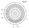
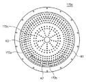
特に、第1及び第2ガス分配プレート170a、170bは、第1及び第2空間a、bで提供される工程ガス及びプラズマの密度が均一に形成されるように非対称に形成される多数のガス噴射流路172a、172bを有する。具体的に、第1及び第2ガス分配プレート170a、170bは、同じ大きさのガス噴射流路172aが形成された第1エッジ部分k1と、基板出入口112と隣接して第1エッジ部分k1に形成されたガス噴射流路172aよりは相対的に大きいガス噴射流路172bが形成された第2エッジ部分k2に区分されることができる非対称のガス噴射流路172a、172bを有する。
In particular, the first and second
図5に示すように、工程チャンバー110は、基板が入り、出ていく基板出入口112によって一側面111aが凹んでいる形態をしている。即ち、基板出入口112によって工程チャンバー110の一側面の厚さほどの空間的な不均一が発生し、これにより、基板出入口112部分では工程チャンバー110内の他の領域とは異なるガス及びプラズマの流れが発生されて基板処理工程の均一な処理が難しくなる問題点が発生する。従って、基板出入口112によるガス及びプラズマの流れ変化による密度不均衡を防止するために、ガス及びプラズマの分配構造を改善する必要性がある。即ち、図5及び図6に示すように、本発明の第1及び第2ガス分配プレート170a、170bは、第2エッジ部分k2に形成されたガス噴射流路172bを通して基板出入口112と隣接した空間では第1エッジ部分k1で提供される量より相対的に多くのプラズマと工程ガスを提供される。このような非対称型のガス噴射流路172a、172bを有する第1及び第2ガス分配プレート170a、170bは、工程チャンバー110の非対称的な空間構造で密度が低い基板出入口112の付近でより多くのプラズマを分配することによって、基板Wエッジに形成されるプラズマ密度を均一化してアッシング均一度を向上させる。第2エッジ部分k2に形成されたガス噴射流路172bの大きさは、第1エッジ部分k1に形成されたガス噴射流路172aに比べて、小さくは1%で、最も大きくは1000%まで開口面積の差を有することが好ましい。参考に、中央部分k3に形成されたガス噴射流路172cは、対称形でに形成され、その大きさは、第2エッジ部分k2に形成されたガス噴射流路172bより相対的に小さなことが好ましい。一方、図9に示したガス分配プレート170dのように、第2エッジ部分k2に形成されたガス噴射流路172bは、スロット形状でもなされることができる。
As shown in FIG. 5, the
図8は、変形されたガス分配プレートを示す図面であり、図7は、本発明に図8に示めすガス分配プレートが適用された例を示す平断面図である。 FIG. 8 is a view showing a modified gas distribution plate, and FIG. 7 is a plan sectional view showing an example in which the gas distribution plate shown in FIG. 8 is applied to the present invention.
図3に示すように、工程チャンバー110の第1及び第2空間a、bでの排気流れを見れば、共通排気管152とダイレクトに連結した排気口116側(区画壁と隣接した領域)が第1、2空間内の他の領域に比べて、ガス及びプラズマの流れが早くなされるため、ガス及びプラズマ密度差が発生される。従って、共通排気管152の影響によるガス及びプラズマの流れ変化による密度不均衡を防止するためにガス及びプラズマの分配構造を改善する必要性がある。図7及び図8のように、第3ガス分配プレート170cは、第2エッジ部分k2に形成されたガス噴射流路172bを通して基板出入口112と隣接した空間で第1エッジ部分k1で提供される量より相対的に多くのプラズマと工程ガスを提供し、特に、共通排気管152と隣接した第3エッジ部分k4に形成されたガス噴射流路172d等を通して共通排気管152と隣接した空間で第1エッジ部分k1で提供される量より相対的に多くのプラズマとガスを提供するようになる。このような非対称型のガス噴射流路172a、172b、172dを有する第3ガス分配プレート170cは、工程チャンバー110の非対称的な空間構造で密度が低い基板出入口112付近と共通排気管152付近でより多くのプラズマとガスを分配することによって、基板Wエッジに形成されるプラズマ密度を均一化してアッシング均一度を向上させる。
As shown in FIG. 3, when the exhaust flow in the first and second spaces a and b of the
図2に示した基板処理装置でのアッシング工程を詳細に説明する。 The ashing process in the substrate processing apparatus shown in FIG. 2 will be described in detail.
図2及び図3に示すように、基板処理装置100の工程が開示されれば、基板Wは、基板出入口112を通して基板支持部材120に各々ローディング(loading)される。基板Wが基板支持部材120にローディングされれば、基板Wは基板支持部材120に提供されたヒーターによって予め設定された温度でに加熱する。そして、電力印加機122は、基板支持部材120各々にバイアス電力を印加する。また、減圧部材156は、工程チャンバー110内部空気を強制吸入して、工程チャンバー110内部圧力を予め設定された圧力でに減圧する。
As shown in FIGS. 2 and 3, when the process of the
工程チャンバー110内部工程圧力及び温度などの工程条件が予め設定された条件を満たせば、プラズマ生成部材140は、プラズマを生成してガス供給部材130で供給し、排気部材150は、工程チャンバー110内部圧力を一定圧力を維持させる。ガス供給部材130を通して噴射されるプラズマは、基板W表面の不必要なレジストを除去する。そして、排気部材150は、工程チャンバー110内部で供給されたプラズマ及び工程ガスを一定流量で排気させ、工程チャンバー110内部圧力を維持する。基板W表面にレジストが除去されれば、基板Wは、基板支持部材120からアンローディング(unloading)された後、基板出入口112を通して工程チャンバー110から搬出される。
If process conditions such as process pressure and temperature inside the
前記基板W表面のレジスト除去工程(アッシング工程)が行われる過程で第1及び第2空間a、bへのプラズマ及びガスの分配は非対称的になる。即ち、工程チャンバー110の非対称的である空間構造で密度が低くなる基板出入口112付近でより多くのプラズマとガスを分配することによって、基板Wエッジに形成されるプラズマ密度を均一化してアッシング均一度を向上させる。
During the process of removing the resist on the surface of the substrate W (ashing process), the distribution of plasma and gas to the first and second spaces a and b becomes asymmetric. That is, the plasma density formed at the edge of the substrate W is made uniform by distributing more plasma and gas in the vicinity of the substrate inlet /
また、第1空間a及び第2空間b各々の排気は独立的になる。即ち、第1空間a内プラズマ及び工程ガスは、区画部材160によって共通排気管152内第1排気空間cに排気され、第2空間b内プラズマ及び工程ガスは、区画部材160によって共通排気管152内第2排気空間dに排気される。この時、第1及び第2空間a、bから排気されるガスは、単一排気管152aによって逆流が防止される。従って、第1空間aと第2空間bに供給されたガスは、互い独立的に分離排気され、第1空間aと第2空間b内プラズマ及びガスの流れは、互い同じ流れを有する。
Moreover, the exhaust of each of the first space a and the second space b is independent. That is, the plasma and process gas in the first space a are exhausted to the first exhaust space c in the
詳述したように、本発明による基板処理装置100は、基板出入口112による非対称的である空間構造を有する工程チャンバー110で基板を処理する時、基板出入口112付近でより多くのプラズマとガスを分配することによって、基板W上に形成されるプラズマ密度を均一化してアッシング均一度を向上させることができる。また、工程チャンバー110内部に複数の支持部材120を備えて複数の基板を同時に処理する時、各々の基板が処理される工程空間を同等な大きさ及び構造、そして支持部材を中心で左右対称になる構造を有するようにハウジング内部を区画することによって、各々の基板上に均一、同等な工程処理を行うことができる。
As described in detail, the
以上の詳細な説明は本発明を例示するものである。また、前述の内容は本発明の好ましい実施形態を表して説明することに過ぎなく、本発明は多様な他の組合、変更及び環境で使用できる。即ち、本明細書に開示された発明の概念の範囲、著述した開示内容と均等な範囲及び/または当業界の技術または知識の範囲内で変更または修正が可能である。前述した一実施形態は、本発明を実施するに最善の状態を説明するためのものであり、本発明と同じ他の発明を利用するに当業界に知られた他の状態への実施、そして発明の具体的な適用分野及び用途で求められる多様な変更も可能である。従って、以上の発明の詳細な説明は開示された実施状態で本発明を制限しようとする意図ではない。また、添付された請求の範囲は他の実施状態も含むことと解析すべきである。 The above detailed description illustrates the invention. Also, the foregoing is merely illustrative of a preferred embodiment of the present invention and the present invention can be used in a variety of other combinations, modifications and environments. That is, changes or modifications can be made within the scope of the concept of the invention disclosed in the present specification, the scope equivalent to the disclosed disclosure, and / or the skill or knowledge of the industry. The above-described embodiment is for explaining the best state for carrying out the present invention, implementation in other states known in the art to utilize the same other invention as the present invention, and Various modifications required in specific application fields and uses of the invention are also possible. Accordingly, the above detailed description of the invention is not intended to limit the invention to the disclosed embodiments. It should also be analyzed that the appended claims include other implementations.
110 工程チャンバー
120 基板支持部材
130 ガス供給部材
140 プラズマ生成部材
150 排気部材
160 区画部材
170a 第1ガス分配プレート
170b 第2ガス分配プレート
110
Claims (5)
基板処理工程が行われるプロセス空間を提供し、かつ一側面に基板の入出のための基板出入口が設けられており、内部に排気口が設けられており、上記基板出入口を開閉するゲートバルブを有する工程チャンバーと、
上記工程チャンバー内部の底側に設けられ、上記基板出入口を通して入ってきた基板が置かれる基板支持部材と、
上記工程チャンバーの上側に設けられており、かつ、上記プロセス空間でプラズマ及び工程ガスを分配するための多数のガス噴射流路を有するガス分配プレートとを含み、
前記ガス分配プレートは、基板出入口と隣接した領域を有しており、
前記基板出入口と隣接した領域に形成された前記ガス噴射流路の直径は、前記基板出入口と隣接した領域以外の領域に形成されたガス噴射流路の直径よりも大きいことを特徴とする基板処理装置。 In substrate processing equipment,
Provided a process space in which a substrate processing process is performed, and provided with a substrate inlet / outlet for entering / exiting a substrate on one side surface, an exhaust port provided therein, and a gate valve for opening / closing the substrate inlet / outlet A process chamber;
A substrate support member provided on the bottom side inside the process chamber and on which a substrate that has entered through the substrate entrance and exit is placed;
A gas distribution plate provided on the upper side of the process chamber and having a plurality of gas injection channels for distributing plasma and process gas in the process space;
The gas distribution plate has a region adjacent to the substrate port;
The diameter of the gas injection flow path formed in the area adjacent to the substrate inlet / outlet is larger than the diameter of the gas injection flow path formed in an area other than the area adjacent to the substrate inlet / outlet. apparatus.
前記ガス分配プレートの上側にプラズマ生成のためのプラズマ源をさらに含むことを特徴とする請求項1に記載の基板処理装置。 The substrate processing apparatus includes:
The substrate processing apparatus of claim 1, further comprising a plasma source for generating plasma on the gas distribution plate.
内部に基板処理工程が行われるプロセス空間を提供し、かつ一側面に基板の入出のための基板出入口を有する工程チャンバーと、
上記工程チャンバー内部に設けられて、工程時に基板を支持する複数の基板支持部材と、
上記基板支持部各々に電力を印加する電力印加機と、
プラズマを発生させて、上記工程チャンバー内部でプラズマを供給するプラズマ生成部材と、
上記工程チャンバー内のガスを排気させる排気部材と、
上記基板支持部材が設けられる上記工程チャンバー内のプロセス空間及び上記排気部材の排気空間を区画する区画部材と、
上記工程チャンバー内の上記プロセス空間上部に設けられており、上記基板支持部材各々に置かれた基板側でプラズマ及び工程ガスを分配するための多数のガス噴射流路を有するガス分配プレートとを含み、
前記ガス分配プレートは、前記基板出入口と隣接した領域を有しており、
前記基板出入口と隣接した領域に形成された前記ガス噴射流路の直径は、他の領域に形成されたガス噴射流路の直径より大きいことを特徴とする基板処理装置。 In an apparatus that performs an ashing process on a substrate,
A process chamber that provides a process space in which substrate processing steps are performed, and has a substrate inlet / outlet for loading / unloading a substrate on one side surface;
A plurality of substrate support members provided inside the process chamber for supporting the substrate during the process;
A power applicator for applying power to each of the substrate supports,
A plasma generating member for generating plasma and supplying plasma inside the process chamber;
An exhaust member for exhausting the gas in the process chamber;
A partition member that partitions a process space in the process chamber in which the substrate support member is provided and an exhaust space of the exhaust member;
A gas distribution plate provided at an upper part of the process space in the process chamber, and having a plurality of gas injection flow paths for distributing plasma and process gas on the substrate side placed on each of the substrate support members. ,
The gas distribution plate has a region adjacent to the substrate inlet and outlet;
The substrate processing apparatus, wherein a diameter of the gas injection channel formed in a region adjacent to the substrate inlet / outlet is larger than a diameter of a gas injection channel formed in another region.
前記工程チャンバーの下部壁で前記基板支持部材各々の中心を基準として環状で形成される排気口を通して前記プロセス空間内のガスを排出させる共通排気管を含み、
前記区画部材は、
上記工程チャンバー内部で上記プロセス空間を区画する区画壁と、
上記プロセス空間各々から排気されるガスが独立的に排気されるように上記共通排気管内の排気空間を区画する隔壁とを含むことを特徴とする請求項3に記載の基板処理装置。 The exhaust member is
A common exhaust pipe for exhausting the gas in the process space through an exhaust port formed in an annular shape with respect to the center of each of the substrate support members at a lower wall of the process chamber;
The partition member is
A partition wall that partitions the process space inside the process chamber;
The substrate processing apparatus according to claim 3 , further comprising a partition wall that partitions the exhaust space in the common exhaust pipe so that the gas exhausted from each of the process spaces is independently exhausted.
前記支持部材の中心を通して前記区画壁と平行する線を中心で左右対称になるように前記工程空間を区画し、
前記隔壁は、
上記隔壁を中心で左右対称になるように前記排気空間を区画することを特徴とする請求項4に記載の基板処理装置。 The partition wall is
Partitioning the process space so as to be symmetrical about a line parallel to the partition wall through the center of the support member;
The partition is
The substrate processing apparatus according to claim 4 , wherein the exhaust space is partitioned so as to be symmetrical about the partition wall.
Applications Claiming Priority (2)
| Application Number | Priority Date | Filing Date | Title |
|---|---|---|---|
| KR1020070005242A KR100796980B1 (en) | 2007-01-17 | 2007-01-17 | Substrate Processing Apparatus and Method |
| KR10-2007-0005242 | 2007-01-17 |
Publications (2)
| Publication Number | Publication Date |
|---|---|
| JP2008177568A JP2008177568A (en) | 2008-07-31 |
| JP4834883B2 true JP4834883B2 (en) | 2011-12-14 |
Family
ID=39218876
Family Applications (1)
| Application Number | Title | Priority Date | Filing Date |
|---|---|---|---|
| JP2008005913A Expired - Fee Related JP4834883B2 (en) | 2007-01-17 | 2008-01-15 | Substrate processing equipment |
Country Status (4)
| Country | Link |
|---|---|
| JP (1) | JP4834883B2 (en) |
| KR (1) | KR100796980B1 (en) |
| CN (1) | CN100590790C (en) |
| TW (1) | TWI394209B (en) |
Families Citing this family (12)
| Publication number | Priority date | Publication date | Assignee | Title |
|---|---|---|---|---|
| KR100851236B1 (en) * | 2007-03-06 | 2008-08-20 | 피에스케이 주식회사 | Exhaust system, substrate processing apparatus including same, and exhaust method |
| KR101057119B1 (en) * | 2009-04-10 | 2011-08-16 | 피에스케이 주식회사 | Exhaust system and substrate processing apparatus having same |
| KR101205242B1 (en) * | 2010-04-30 | 2012-11-27 | 주식회사 테라세미콘 | Plasma processing apparatus |
| KR20140122548A (en) * | 2013-04-10 | 2014-10-20 | 피에스케이 주식회사 | Apparatus and method for providing power, and apparatus for treating substrate using the same |
| KR101445226B1 (en) * | 2013-04-23 | 2014-09-29 | 피에스케이 주식회사 | Exhaust ring assembly and apparatus for treating including the assembly |
| KR101546447B1 (en) | 2014-03-20 | 2015-08-25 | 피에스케이 주식회사 | Baffle and substrate treating apparatus including the baffle |
| CN106935530B (en) | 2015-12-31 | 2020-04-17 | 中微半导体设备(上海)股份有限公司 | Plasma etching photoresist device |
| US20180185893A1 (en) * | 2016-12-31 | 2018-07-05 | Applied Materials, Inc. | Systems, methods, and apparatus for transfer chamber gas purge of electronic device processing systems |
| KR102187121B1 (en) | 2019-04-30 | 2020-12-07 | 피에스케이 주식회사 | A substrate processing apparatus |
| CN112216586B (en) * | 2019-07-12 | 2023-03-10 | 中微半导体设备(上海)股份有限公司 | Double-station processor for realizing uniform exhaust and plasma processing equipment |
| CN112509903B (en) * | 2020-12-17 | 2025-05-16 | 上海谙邦半导体设备有限公司 | Plasma processing device |
| KR102898045B1 (en) * | 2023-08-09 | 2025-12-09 | 피에스케이 주식회사 | Substrate processing apparatus and substrate processing method |
Family Cites Families (13)
| Publication number | Priority date | Publication date | Assignee | Title |
|---|---|---|---|---|
| JPS58185498A (en) | 1982-04-21 | 1983-10-29 | Clarion Co Ltd | Device for growing thin film in vaper phase |
| JPH0210828A (en) * | 1988-06-29 | 1990-01-16 | Matsushita Electric Ind Co Ltd | Etching device and method thereof |
| JPH02115359A (en) * | 1988-10-25 | 1990-04-27 | Dainippon Printing Co Ltd | Compound thin film production method and device |
| US6077157A (en) * | 1996-11-18 | 2000-06-20 | Applied Materials, Inc. | Process chamber exhaust system |
| JPH10242118A (en) * | 1997-02-27 | 1998-09-11 | Matsushita Electron Corp | Apparatus for manufacturing semiconductor device |
| JP3531466B2 (en) * | 1998-03-26 | 2004-05-31 | 松下電器産業株式会社 | Semiconductor device manufacturing equipment |
| JP2000030894A (en) * | 1998-07-07 | 2000-01-28 | Kokusai Electric Co Ltd | Plasma processing method and apparatus |
| JP3002448B1 (en) * | 1998-07-31 | 2000-01-24 | 国際電気株式会社 | Substrate processing equipment |
| JP2002212786A (en) * | 2001-01-17 | 2002-07-31 | Ebara Corp | Substrate processing equipment |
| KR100442580B1 (en) * | 2001-10-09 | 2004-08-02 | 주성엔지니어링(주) | air exhaust system of chamber for semiconductor manufacture |
| KR100442310B1 (en) * | 2001-11-28 | 2004-07-30 | 최우범 | Wafer bonding machine with plasma treatment and control method thereof |
| US8580076B2 (en) * | 2003-05-22 | 2013-11-12 | Lam Research Corporation | Plasma apparatus, gas distribution assembly for a plasma apparatus and processes therewith |
| KR20040102600A (en) * | 2003-05-28 | 2004-12-08 | 삼성전자주식회사 | Deposition apparatus for manufacturing semiconductor devices |
-
2007
- 2007-01-17 KR KR1020070005242A patent/KR100796980B1/en not_active Expired - Fee Related
-
2008
- 2008-01-04 CN CN200810000424A patent/CN100590790C/en not_active Expired - Fee Related
- 2008-01-15 JP JP2008005913A patent/JP4834883B2/en not_active Expired - Fee Related
- 2008-01-16 TW TW097101627A patent/TWI394209B/en not_active IP Right Cessation
Also Published As
| Publication number | Publication date |
|---|---|
| CN101226875A (en) | 2008-07-23 |
| TWI394209B (en) | 2013-04-21 |
| JP2008177568A (en) | 2008-07-31 |
| TW200834708A (en) | 2008-08-16 |
| KR100796980B1 (en) | 2008-01-22 |
| CN100590790C (en) | 2010-02-17 |
Similar Documents
| Publication | Publication Date | Title |
|---|---|---|
| JP4834883B2 (en) | Substrate processing equipment | |
| US10822695B2 (en) | Thin film deposition apparatus | |
| US10190214B2 (en) | Deposition apparatus and deposition system having the same | |
| TWI760438B (en) | Method and apparatus of remote plasmas flowable cvd chamber | |
| KR101445226B1 (en) | Exhaust ring assembly and apparatus for treating including the assembly | |
| KR100939933B1 (en) | Lift pin assembly and substrate processing apparatus having the same | |
| WO2011125471A1 (en) | Plasma processing device and plasma processing method | |
| KR101477602B1 (en) | Apparatus for treatimg substrate | |
| TWI831846B (en) | Substrate processing apparatus | |
| KR20210022196A (en) | Apparatus for treating substrate | |
| JP6602271B2 (en) | Substrate processing apparatus and substrate processing method | |
| KR102121598B1 (en) | A baffle assembly and an apparatus for treating a substrate with the baffle | |
| JP6954565B2 (en) | Board processing equipment | |
| KR100830850B1 (en) | Substrate processing equipment | |
| KR101905640B1 (en) | Apparatus for treating substrate | |
| CN119061379A (en) | Shower head, substrate processing device and substrate processing method | |
| KR100737749B1 (en) | Remote Plasma Ashing Device and Method | |
| CN119343764A (en) | Cleaning throttle valves and foreline using a microwave source | |
| KR100837625B1 (en) | Substrate Processing Apparatus and Method | |
| KR100810457B1 (en) | Substrate Processing Apparatus and Method | |
| KR100647257B1 (en) | Heating chuck for semiconductor manufacturing with heat transfer gas supply structure | |
| US20060112877A1 (en) | Nozzle and plasma apparatus incorporating the nozzle | |
| KR100444753B1 (en) | Deposition apparatus for manufacturing semiconductor devices | |
| KR101276256B1 (en) | Substrate treating apparatus and method | |
| KR100750828B1 (en) | Substrate Ashing Device |
Legal Events
| Date | Code | Title | Description |
|---|---|---|---|
| A977 | Report on retrieval |
Free format text: JAPANESE INTERMEDIATE CODE: A971007 Effective date: 20101111 |
|
| A131 | Notification of reasons for refusal |
Free format text: JAPANESE INTERMEDIATE CODE: A131 Effective date: 20101124 |
|
| A521 | Written amendment |
Free format text: JAPANESE INTERMEDIATE CODE: A523 Effective date: 20110224 |
|
| A131 | Notification of reasons for refusal |
Free format text: JAPANESE INTERMEDIATE CODE: A131 Effective date: 20110329 |
|
| A521 | Written amendment |
Free format text: JAPANESE INTERMEDIATE CODE: A523 Effective date: 20110629 |
|
| TRDD | Decision of grant or rejection written | ||
| A01 | Written decision to grant a patent or to grant a registration (utility model) |
Free format text: JAPANESE INTERMEDIATE CODE: A01 Effective date: 20110809 |
|
| A01 | Written decision to grant a patent or to grant a registration (utility model) |
Free format text: JAPANESE INTERMEDIATE CODE: A01 |
|
| A61 | First payment of annual fees (during grant procedure) |
Free format text: JAPANESE INTERMEDIATE CODE: A61 Effective date: 20110908 |
|
| FPAY | Renewal fee payment (event date is renewal date of database) |
Free format text: PAYMENT UNTIL: 20141007 Year of fee payment: 3 |
|
| R150 | Certificate of patent or registration of utility model |
Free format text: JAPANESE INTERMEDIATE CODE: R150 |
|
| R250 | Receipt of annual fees |
Free format text: JAPANESE INTERMEDIATE CODE: R250 |
|
| R250 | Receipt of annual fees |
Free format text: JAPANESE INTERMEDIATE CODE: R250 |
|
| R250 | Receipt of annual fees |
Free format text: JAPANESE INTERMEDIATE CODE: R250 |
|
| LAPS | Cancellation because of no payment of annual fees |