JP4866176B2 - 走査型電子顕微鏡を備えたプローバ装置及びプローバ装置の探針クリーニング方法 - Google Patents
走査型電子顕微鏡を備えたプローバ装置及びプローバ装置の探針クリーニング方法 Download PDFInfo
- Publication number
- JP4866176B2 JP4866176B2 JP2006225563A JP2006225563A JP4866176B2 JP 4866176 B2 JP4866176 B2 JP 4866176B2 JP 2006225563 A JP2006225563 A JP 2006225563A JP 2006225563 A JP2006225563 A JP 2006225563A JP 4866176 B2 JP4866176 B2 JP 4866176B2
- Authority
- JP
- Japan
- Prior art keywords
- probe
- integrated circuit
- cleaning
- unit
- electron microscope
- Prior art date
- Legal status (The legal status is an assumption and is not a legal conclusion. Google has not performed a legal analysis and makes no representation as to the accuracy of the status listed.)
- Expired - Fee Related
Links
Images


Landscapes
- Measuring Leads Or Probes (AREA)
- Tests Of Electronic Circuits (AREA)
- Testing Or Measuring Of Semiconductors Or The Like (AREA)
Description
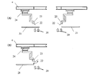
図1は、本発明の第1の実施形態が適用された走査型電子顕微鏡の要部構成図である。走査型電子顕微鏡は、電子線を制御する鏡筒1の試料室2(一部を破断して示し、ゲート弁6が形成されている)において試料を出し入れするための、仕込み室3(一部を破断して示し、試料ウエハ13が配置されている)及びプローブユニット4をクリーニングする真空排気装置7を備えている。
他のクリーニング手段としては、酸素プラズマを利用するドライエッチング(10−1〜10−3Pa)等,真空中での砥粒の細かい砥石やヤスリなどに、探針を押しあてての機械的な研磨,先端部を曲げることにより酸化膜を剥離する方法、切断することにより酸化膜等のない表面を出現させる方法でも良い。
次に、本発明の第2の実施形態について説明する。第2の実施形態である走査型電子顕微鏡の概略構成は、第1の実施形態と同様であるので、説明は省略する。
ここで、実際の半導体集積回路を作製したウエハ上の電極に探針を当てて試験をしている際に、導通がとれなくなってくる探針があったので、金メッキ付の試験ウエハ13を用いて、探針22を接触させて導通チェックをおこなった。
次に、本発明の第3の実施形態について、説明する。図5は、本発明の第3の実施形態である走査型電子顕微鏡の要部構成図である。この第3の実施形態と第1の実施形態との相違点は、第3の実施形態にはクリーニング室5に予備室26が設けられている点である。この予備室26は、探針22を大気に暴露させる機会を、さらに減らすために設けられている。
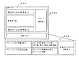
(2)プローブユニット17の行き先及び状態表示
(3)クリーニング室5内のミリングの条件設定(ガス量、電圧、電流、処理時間)とそのモニタ表示
(4)クリーニング周期設定とその表示及びクリーニング回数の記憶
(5)評価サンプルでの結果表示
なお、クリーニング処理及びクリーニング後の探針表面状態の評価を自動で行う場合には、上記の(3)及び(4)の設定を行うレシピを追加して使用する。
Claims (2)
- 走査型電子顕微鏡により観察しながら、真空中で半導体集積回路に接触させる探針を有する探針ユニットを備え、上記半導体集積回路の電気的特性を測定するプローバ装置において、
真空中で、上記探針ユニットの探針を半導体集積回路に接触させる試料室と、
上記試料室に配置された探針ユニットの探針からの信号に基づいて、上記探針の電気的導通状態を判断する判断部と、
上記探針ユニットに設けられ、探針を回動させる探針回動手段と、
不活性ガスイオンを上記探針に照射するイオン源を有し、上記判断部で電気的導通状態が不良と判断された探針を上記探針回動手段により回動し、不活性ガスイオンを照射して、この短針をクリーニングするクリーニング室と、
を備えること特徴とするプローバ装置。 - 走査型電子顕微鏡により観察しながら、真空中で半導体集積回路に探針を接触させ、この探針から得られる電気信号に基づいて、上記半導体集積回路の電気的特性を測定するプローバ装置の探針クリーニング方法において、
真空の試料室内で、上記探針を半導体集積回路に接触させ、
上記試料室内の試験用半導体集積回路に接触された探針からの信号に基づいて、上記探針の電気的導通状態を判断し、
電気的導通状態が不良と判断された探針を真空中で回動させながら、不活性ガスイオンを上記探針に照射してこの探針をクリーニングすることを特徴とするプローバ装置の探針クリーニング方法。
Priority Applications (1)
| Application Number | Priority Date | Filing Date | Title |
|---|---|---|---|
| JP2006225563A JP4866176B2 (ja) | 2006-08-22 | 2006-08-22 | 走査型電子顕微鏡を備えたプローバ装置及びプローバ装置の探針クリーニング方法 |
Applications Claiming Priority (1)
| Application Number | Priority Date | Filing Date | Title |
|---|---|---|---|
| JP2006225563A JP4866176B2 (ja) | 2006-08-22 | 2006-08-22 | 走査型電子顕微鏡を備えたプローバ装置及びプローバ装置の探針クリーニング方法 |
Related Child Applications (1)
| Application Number | Title | Priority Date | Filing Date |
|---|---|---|---|
| JP2010275690A Division JP5133394B2 (ja) | 2010-12-10 | 2010-12-10 | 走査型電子顕微鏡を備えたプローバ装置及びプローバ装置の探針クリーニング方法 |
Publications (2)
| Publication Number | Publication Date |
|---|---|
| JP2008051547A JP2008051547A (ja) | 2008-03-06 |
| JP4866176B2 true JP4866176B2 (ja) | 2012-02-01 |
Family
ID=39235759
Family Applications (1)
| Application Number | Title | Priority Date | Filing Date |
|---|---|---|---|
| JP2006225563A Expired - Fee Related JP4866176B2 (ja) | 2006-08-22 | 2006-08-22 | 走査型電子顕微鏡を備えたプローバ装置及びプローバ装置の探針クリーニング方法 |
Country Status (1)
| Country | Link |
|---|---|
| JP (1) | JP4866176B2 (ja) |
Families Citing this family (4)
| Publication number | Priority date | Publication date | Assignee | Title |
|---|---|---|---|---|
| KR102804323B1 (ko) * | 2018-06-20 | 2025-05-08 | 피직 인스트루멘테 (페 이) 에스 에 운트 코. 카게 | 센서 프로브 조립체 |
| JP7503915B2 (ja) * | 2020-02-28 | 2024-06-21 | 富士紡ホールディングス株式会社 | クリーニングシート |
| CN112349635B (zh) * | 2020-10-23 | 2024-10-18 | 杭州长川科技股份有限公司 | 晶圆与清针片存放装置 |
| JP2023178889A (ja) * | 2022-06-06 | 2023-12-18 | 東京エレクトロン株式会社 | 情報処理装置、表示入力装置およびプログラム |
Family Cites Families (4)
| Publication number | Priority date | Publication date | Assignee | Title |
|---|---|---|---|---|
| JP3577839B2 (ja) * | 1996-06-04 | 2004-10-20 | 株式会社日立製作所 | 不良検査方法および装置 |
| JPH10185953A (ja) * | 1996-12-27 | 1998-07-14 | Mitsubishi Electric Corp | プローブカード探針の洗浄方法およびこの洗浄方法を実施するための装置 |
| JPH10209231A (ja) * | 1997-01-17 | 1998-08-07 | Nippon Steel Corp | プローブ装置及びプローブ装置による検査方法 |
| JP2002181898A (ja) * | 2000-12-11 | 2002-06-26 | Hitachi Ltd | プローブ装置 |
-
2006
- 2006-08-22 JP JP2006225563A patent/JP4866176B2/ja not_active Expired - Fee Related
Also Published As
| Publication number | Publication date |
|---|---|
| JP2008051547A (ja) | 2008-03-06 |
Similar Documents
| Publication | Publication Date | Title |
|---|---|---|
| TWI696219B (zh) | 清理方法及電漿處理方法 | |
| EP0951578B1 (en) | Precision etching and coating system | |
| US7750654B2 (en) | Probe method, prober, and electrode reducing/plasma-etching processing mechanism | |
| EP2916344B1 (en) | Method of cleaning a plasma processing apparatus | |
| JP5133394B2 (ja) | 走査型電子顕微鏡を備えたプローバ装置及びプローバ装置の探針クリーニング方法 | |
| US7875156B2 (en) | Probe storage container, prober apparatus, probe arranging method and manufacturing method of probe storage container | |
| TW202020237A (zh) | 陽極氧化鈦材及其製造方法 | |
| JP4205122B2 (ja) | 荷電粒子線加工装置 | |
| US20050224457A1 (en) | Method and apparatus for repairing shape, and method for manufacturing semiconductor device using those | |
| JP4866176B2 (ja) | 走査型電子顕微鏡を備えたプローバ装置及びプローバ装置の探針クリーニング方法 | |
| Zudhistira et al. | Precision Xe plasma FIB delayering for physical failure analysis of sub-20 nm microprocessor devices | |
| JP2019029593A (ja) | プローブ装置 | |
| JPH10163280A (ja) | 検査方法及び検査装置 | |
| US20190164719A1 (en) | Ion source and electron source having single-atom termination structure, tip having single-atom termination structure, gas field ion source, focused ion beam apparatus, electron source, electron microscope, mask repair apparatus, and method of manufacturing tip having single-atom termination structure | |
| TW466729B (en) | Plating method and device, and plating system | |
| CN1695238B (zh) | 探测方法、探测器和电极还原/等离子体刻蚀处理机构 | |
| JP4792404B2 (ja) | 電子源の製造方法 | |
| JPH1074734A (ja) | プラズマ処理装置と半導体装置の製造方法 | |
| JP2002181898A (ja) | プローブ装置 | |
| TWI380360B (ja) | ||
| Zudhistira et al. | Integration of probing capability into plasma FIB for in-situ Delayering, defect inspection, and EBAC on BEOL defects of sub-20nm FinFET devices | |
| JP3453325B2 (ja) | 半導体装置およびその製造方法 | |
| JP6937941B2 (ja) | 真空インタラプタ | |
| JP2008046324A (ja) | 顕微鏡微細作業用マイクロマニピュレーション装置 | |
| Pupeter et al. | Comparative studies on enhanced field emission from mechanically and chemically polished broad-area Nb, Cu, and Al cathodes |
Legal Events
| Date | Code | Title | Description |
|---|---|---|---|
| A621 | Written request for application examination |
Free format text: JAPANESE INTERMEDIATE CODE: A621 Effective date: 20080513 |
|
| A977 | Report on retrieval |
Free format text: JAPANESE INTERMEDIATE CODE: A971007 Effective date: 20100715 |
|
| A131 | Notification of reasons for refusal |
Free format text: JAPANESE INTERMEDIATE CODE: A131 Effective date: 20100727 |
|
| A521 | Request for written amendment filed |
Free format text: JAPANESE INTERMEDIATE CODE: A523 Effective date: 20100924 |
|
| A131 | Notification of reasons for refusal |
Free format text: JAPANESE INTERMEDIATE CODE: A131 Effective date: 20101012 |
|
| A521 | Request for written amendment filed |
Free format text: JAPANESE INTERMEDIATE CODE: A523 Effective date: 20101210 |
|
| A131 | Notification of reasons for refusal |
Free format text: JAPANESE INTERMEDIATE CODE: A131 Effective date: 20110823 |
|
| A521 | Request for written amendment filed |
Free format text: JAPANESE INTERMEDIATE CODE: A523 Effective date: 20111019 |
|
| TRDD | Decision of grant or rejection written | ||
| A01 | Written decision to grant a patent or to grant a registration (utility model) |
Free format text: JAPANESE INTERMEDIATE CODE: A01 Effective date: 20111108 |
|
| A01 | Written decision to grant a patent or to grant a registration (utility model) |
Free format text: JAPANESE INTERMEDIATE CODE: A01 |
|
| A61 | First payment of annual fees (during grant procedure) |
Free format text: JAPANESE INTERMEDIATE CODE: A61 Effective date: 20111111 |
|
| FPAY | Renewal fee payment (event date is renewal date of database) |
Free format text: PAYMENT UNTIL: 20141118 Year of fee payment: 3 |
|
| R150 | Certificate of patent or registration of utility model |
Ref document number: 4866176 Country of ref document: JP Free format text: JAPANESE INTERMEDIATE CODE: R150 Free format text: JAPANESE INTERMEDIATE CODE: R150 |
|
| S531 | Written request for registration of change of domicile |
Free format text: JAPANESE INTERMEDIATE CODE: R313531 |
|
| S533 | Written request for registration of change of name |
Free format text: JAPANESE INTERMEDIATE CODE: R313533 |
|
| R350 | Written notification of registration of transfer |
Free format text: JAPANESE INTERMEDIATE CODE: R350 |
|
| LAPS | Cancellation because of no payment of annual fees |