JP4905914B2 - 多層反射膜付き基板、その製造方法、反射型マスクブランクおよび反射型マスク - Google Patents
多層反射膜付き基板、その製造方法、反射型マスクブランクおよび反射型マスク Download PDFInfo
- Publication number
- JP4905914B2 JP4905914B2 JP2005300556A JP2005300556A JP4905914B2 JP 4905914 B2 JP4905914 B2 JP 4905914B2 JP 2005300556 A JP2005300556 A JP 2005300556A JP 2005300556 A JP2005300556 A JP 2005300556A JP 4905914 B2 JP4905914 B2 JP 4905914B2
- Authority
- JP
- Japan
- Prior art keywords
- film
- substrate
- multilayer
- multilayer reflective
- reflective film
- Prior art date
- Legal status (The legal status is an assumption and is not a legal conclusion. Google has not performed a legal analysis and makes no representation as to the accuracy of the status listed.)
- Expired - Fee Related
Links
Images


Classifications
-
- G—PHYSICS
- G03—PHOTOGRAPHY; CINEMATOGRAPHY; ANALOGOUS TECHNIQUES USING WAVES OTHER THAN OPTICAL WAVES; ELECTROGRAPHY; HOLOGRAPHY
- G03F—PHOTOMECHANICAL PRODUCTION OF TEXTURED OR PATTERNED SURFACES, e.g. FOR PRINTING, FOR PROCESSING OF SEMICONDUCTOR DEVICES; MATERIALS THEREFOR; ORIGINALS THEREFOR; APPARATUS SPECIALLY ADAPTED THEREFOR
- G03F1/00—Originals for photomechanical production of textured or patterned surfaces, e.g., masks, photo-masks, reticles; Mask blanks or pellicles therefor; Containers specially adapted therefor; Preparation thereof
- G03F1/22—Masks or mask blanks for imaging by radiation of 100nm or shorter wavelength, e.g. X-ray masks, extreme ultraviolet [EUV] masks; Preparation thereof
- G03F1/24—Reflection masks; Preparation thereof
-
- G—PHYSICS
- G02—OPTICS
- G02B—OPTICAL ELEMENTS, SYSTEMS OR APPARATUS
- G02B5/00—Optical elements other than lenses
- G02B5/08—Mirrors
- G02B5/0891—Ultraviolet [UV] mirrors
-
- B—PERFORMING OPERATIONS; TRANSPORTING
- B82—NANOTECHNOLOGY
- B82Y—SPECIFIC USES OR APPLICATIONS OF NANOSTRUCTURES; MEASUREMENT OR ANALYSIS OF NANOSTRUCTURES; MANUFACTURE OR TREATMENT OF NANOSTRUCTURES
- B82Y10/00—Nanotechnology for information processing, storage or transmission, e.g. quantum computing or single electron logic
-
- B—PERFORMING OPERATIONS; TRANSPORTING
- B82—NANOTECHNOLOGY
- B82Y—SPECIFIC USES OR APPLICATIONS OF NANOSTRUCTURES; MEASUREMENT OR ANALYSIS OF NANOSTRUCTURES; MANUFACTURE OR TREATMENT OF NANOSTRUCTURES
- B82Y40/00—Manufacture or treatment of nanostructures
-
- C—CHEMISTRY; METALLURGY
- C03—GLASS; MINERAL OR SLAG WOOL
- C03C—CHEMICAL COMPOSITION OF GLASSES, GLAZES OR VITREOUS ENAMELS; SURFACE TREATMENT OF GLASS; SURFACE TREATMENT OF FIBRES OR FILAMENTS MADE FROM GLASS, MINERALS OR SLAGS; JOINING GLASS TO GLASS OR OTHER MATERIALS
- C03C17/00—Surface treatment of glass, not in the form of fibres or filaments, by coating
- C03C17/34—Surface treatment of glass, not in the form of fibres or filaments, by coating with at least two coatings having different compositions
- C03C17/36—Surface treatment of glass, not in the form of fibres or filaments, by coating with at least two coatings having different compositions at least one coating being a metal
-
- C—CHEMISTRY; METALLURGY
- C03—GLASS; MINERAL OR SLAG WOOL
- C03C—CHEMICAL COMPOSITION OF GLASSES, GLAZES OR VITREOUS ENAMELS; SURFACE TREATMENT OF GLASS; SURFACE TREATMENT OF FIBRES OR FILAMENTS MADE FROM GLASS, MINERALS OR SLAGS; JOINING GLASS TO GLASS OR OTHER MATERIALS
- C03C17/00—Surface treatment of glass, not in the form of fibres or filaments, by coating
- C03C17/34—Surface treatment of glass, not in the form of fibres or filaments, by coating with at least two coatings having different compositions
- C03C17/36—Surface treatment of glass, not in the form of fibres or filaments, by coating with at least two coatings having different compositions at least one coating being a metal
- C03C17/3602—Surface treatment of glass, not in the form of fibres or filaments, by coating with at least two coatings having different compositions at least one coating being a metal the metal being present as a layer
- C03C17/3613—Coatings of type glass/inorganic compound/metal/inorganic compound/metal/other
-
- C—CHEMISTRY; METALLURGY
- C03—GLASS; MINERAL OR SLAG WOOL
- C03C—CHEMICAL COMPOSITION OF GLASSES, GLAZES OR VITREOUS ENAMELS; SURFACE TREATMENT OF GLASS; SURFACE TREATMENT OF FIBRES OR FILAMENTS MADE FROM GLASS, MINERALS OR SLAGS; JOINING GLASS TO GLASS OR OTHER MATERIALS
- C03C17/00—Surface treatment of glass, not in the form of fibres or filaments, by coating
- C03C17/34—Surface treatment of glass, not in the form of fibres or filaments, by coating with at least two coatings having different compositions
- C03C17/36—Surface treatment of glass, not in the form of fibres or filaments, by coating with at least two coatings having different compositions at least one coating being a metal
- C03C17/3602—Surface treatment of glass, not in the form of fibres or filaments, by coating with at least two coatings having different compositions at least one coating being a metal the metal being present as a layer
- C03C17/3615—Coatings of the type glass/metal/other inorganic layers, at least one layer being non-metallic
-
- C—CHEMISTRY; METALLURGY
- C03—GLASS; MINERAL OR SLAG WOOL
- C03C—CHEMICAL COMPOSITION OF GLASSES, GLAZES OR VITREOUS ENAMELS; SURFACE TREATMENT OF GLASS; SURFACE TREATMENT OF FIBRES OR FILAMENTS MADE FROM GLASS, MINERALS OR SLAGS; JOINING GLASS TO GLASS OR OTHER MATERIALS
- C03C17/00—Surface treatment of glass, not in the form of fibres or filaments, by coating
- C03C17/34—Surface treatment of glass, not in the form of fibres or filaments, by coating with at least two coatings having different compositions
- C03C17/36—Surface treatment of glass, not in the form of fibres or filaments, by coating with at least two coatings having different compositions at least one coating being a metal
- C03C17/3602—Surface treatment of glass, not in the form of fibres or filaments, by coating with at least two coatings having different compositions at least one coating being a metal the metal being present as a layer
- C03C17/3636—Surface treatment of glass, not in the form of fibres or filaments, by coating with at least two coatings having different compositions at least one coating being a metal the metal being present as a layer one layer at least containing silicon, hydrogenated silicon or a silicide
-
- C—CHEMISTRY; METALLURGY
- C03—GLASS; MINERAL OR SLAG WOOL
- C03C—CHEMICAL COMPOSITION OF GLASSES, GLAZES OR VITREOUS ENAMELS; SURFACE TREATMENT OF GLASS; SURFACE TREATMENT OF FIBRES OR FILAMENTS MADE FROM GLASS, MINERALS OR SLAGS; JOINING GLASS TO GLASS OR OTHER MATERIALS
- C03C17/00—Surface treatment of glass, not in the form of fibres or filaments, by coating
- C03C17/34—Surface treatment of glass, not in the form of fibres or filaments, by coating with at least two coatings having different compositions
- C03C17/36—Surface treatment of glass, not in the form of fibres or filaments, by coating with at least two coatings having different compositions at least one coating being a metal
- C03C17/3602—Surface treatment of glass, not in the form of fibres or filaments, by coating with at least two coatings having different compositions at least one coating being a metal the metal being present as a layer
- C03C17/3639—Multilayers containing at least two functional metal layers
-
- C—CHEMISTRY; METALLURGY
- C03—GLASS; MINERAL OR SLAG WOOL
- C03C—CHEMICAL COMPOSITION OF GLASSES, GLAZES OR VITREOUS ENAMELS; SURFACE TREATMENT OF GLASS; SURFACE TREATMENT OF FIBRES OR FILAMENTS MADE FROM GLASS, MINERALS OR SLAGS; JOINING GLASS TO GLASS OR OTHER MATERIALS
- C03C17/00—Surface treatment of glass, not in the form of fibres or filaments, by coating
- C03C17/34—Surface treatment of glass, not in the form of fibres or filaments, by coating with at least two coatings having different compositions
- C03C17/36—Surface treatment of glass, not in the form of fibres or filaments, by coating with at least two coatings having different compositions at least one coating being a metal
- C03C17/3602—Surface treatment of glass, not in the form of fibres or filaments, by coating with at least two coatings having different compositions at least one coating being a metal the metal being present as a layer
- C03C17/3649—Surface treatment of glass, not in the form of fibres or filaments, by coating with at least two coatings having different compositions at least one coating being a metal the metal being present as a layer made of metals other than silver
-
- C—CHEMISTRY; METALLURGY
- C03—GLASS; MINERAL OR SLAG WOOL
- C03C—CHEMICAL COMPOSITION OF GLASSES, GLAZES OR VITREOUS ENAMELS; SURFACE TREATMENT OF GLASS; SURFACE TREATMENT OF FIBRES OR FILAMENTS MADE FROM GLASS, MINERALS OR SLAGS; JOINING GLASS TO GLASS OR OTHER MATERIALS
- C03C17/00—Surface treatment of glass, not in the form of fibres or filaments, by coating
- C03C17/34—Surface treatment of glass, not in the form of fibres or filaments, by coating with at least two coatings having different compositions
- C03C17/36—Surface treatment of glass, not in the form of fibres or filaments, by coating with at least two coatings having different compositions at least one coating being a metal
- C03C17/3602—Surface treatment of glass, not in the form of fibres or filaments, by coating with at least two coatings having different compositions at least one coating being a metal the metal being present as a layer
- C03C17/3657—Surface treatment of glass, not in the form of fibres or filaments, by coating with at least two coatings having different compositions at least one coating being a metal the metal being present as a layer the multilayer coating having optical properties
- C03C17/3665—Surface treatment of glass, not in the form of fibres or filaments, by coating with at least two coatings having different compositions at least one coating being a metal the metal being present as a layer the multilayer coating having optical properties specially adapted for use as photomask
-
- C—CHEMISTRY; METALLURGY
- C03—GLASS; MINERAL OR SLAG WOOL
- C03C—CHEMICAL COMPOSITION OF GLASSES, GLAZES OR VITREOUS ENAMELS; SURFACE TREATMENT OF GLASS; SURFACE TREATMENT OF FIBRES OR FILAMENTS MADE FROM GLASS, MINERALS OR SLAGS; JOINING GLASS TO GLASS OR OTHER MATERIALS
- C03C17/00—Surface treatment of glass, not in the form of fibres or filaments, by coating
- C03C17/34—Surface treatment of glass, not in the form of fibres or filaments, by coating with at least two coatings having different compositions
- C03C17/36—Surface treatment of glass, not in the form of fibres or filaments, by coating with at least two coatings having different compositions at least one coating being a metal
- C03C17/40—Surface treatment of glass, not in the form of fibres or filaments, by coating with at least two coatings having different compositions at least one coating being a metal all coatings being metal coatings
-
- G—PHYSICS
- G02—OPTICS
- G02B—OPTICAL ELEMENTS, SYSTEMS OR APPARATUS
- G02B5/00—Optical elements other than lenses
- G02B5/08—Mirrors
- G02B5/0816—Multilayer mirrors, i.e. having two or more reflecting layers
- G02B5/085—Multilayer mirrors, i.e. having two or more reflecting layers at least one of the reflecting layers comprising metal
- G02B5/0875—Multilayer mirrors, i.e. having two or more reflecting layers at least one of the reflecting layers comprising metal the reflecting layers comprising two or more metallic layers
-
- G—PHYSICS
- G21—NUCLEAR PHYSICS; NUCLEAR ENGINEERING
- G21K—HANDLING OF PARTICLES OR IONISING RADIATION NOT OTHERWISE PROVIDED FOR; IRRADIATION DEVICES; GAMMA RAY OR X-RAY MICROSCOPES
- G21K1/00—Arrangements for handling particles or ionising radiation, e.g. focusing or moderating
- G21K1/06—Arrangements for handling particles or ionising radiation, e.g. focusing or moderating using diffraction, refraction or reflection, e.g. monochromators
- G21K1/062—Devices having a multilayer structure
-
- C—CHEMISTRY; METALLURGY
- C03—GLASS; MINERAL OR SLAG WOOL
- C03C—CHEMICAL COMPOSITION OF GLASSES, GLAZES OR VITREOUS ENAMELS; SURFACE TREATMENT OF GLASS; SURFACE TREATMENT OF FIBRES OR FILAMENTS MADE FROM GLASS, MINERALS OR SLAGS; JOINING GLASS TO GLASS OR OTHER MATERIALS
- C03C2217/00—Coatings on glass
- C03C2217/70—Properties of coatings
- C03C2217/73—Anti-reflective coatings with specific characteristics
- C03C2217/734—Anti-reflective coatings with specific characteristics comprising an alternation of high and low refractive indexes
-
- G—PHYSICS
- G21—NUCLEAR PHYSICS; NUCLEAR ENGINEERING
- G21K—HANDLING OF PARTICLES OR IONISING RADIATION NOT OTHERWISE PROVIDED FOR; IRRADIATION DEVICES; GAMMA RAY OR X-RAY MICROSCOPES
- G21K2201/00—Arrangements for handling radiation or particles
- G21K2201/06—Arrangements for handling radiation or particles using diffractive, refractive or reflecting elements
- G21K2201/067—Construction details
Landscapes
- Chemical & Material Sciences (AREA)
- Engineering & Computer Science (AREA)
- Chemical Kinetics & Catalysis (AREA)
- Geochemistry & Mineralogy (AREA)
- Organic Chemistry (AREA)
- Materials Engineering (AREA)
- Life Sciences & Earth Sciences (AREA)
- General Chemical & Material Sciences (AREA)
- Physics & Mathematics (AREA)
- Nanotechnology (AREA)
- General Physics & Mathematics (AREA)
- Crystallography & Structural Chemistry (AREA)
- Optics & Photonics (AREA)
- Mathematical Physics (AREA)
- Condensed Matter Physics & Semiconductors (AREA)
- Theoretical Computer Science (AREA)
- Manufacturing & Machinery (AREA)
- Spectroscopy & Molecular Physics (AREA)
- General Engineering & Computer Science (AREA)
- High Energy & Nuclear Physics (AREA)
- Exposure Of Semiconductors, Excluding Electron Or Ion Beam Exposure (AREA)
- Preparing Plates And Mask In Photomechanical Process (AREA)
- Optical Elements Other Than Lenses (AREA)
- Exposure And Positioning Against Photoresist Photosensitive Materials (AREA)
Description
したがって、基板の表面粗さに対する要求は厳しく、例えば二乗平均平方根粗さ(Rms)で0.10nm以下であることが望ましいとされている。
本発明は、かかる知見に基づいて完成したものである。
(1) 基板上に、Mo膜とSi膜を1周期としてこれを複数周期積層させたMo/Siの交互積層膜からなる多層下地膜および露光光を反射する、Mo膜とSi膜を1周期としてこれを複数周期積層させたMo/Siの交互積層膜からなる多層反射膜を順次設けてなり、EUV光を露光光とするリソグラフィー法で使用される多層反射膜付き基板であって、前記多層下地膜の周期長をdbottom[単位:nm]、多層反射膜の周期長をdtop[単位:nm]とした場合、dbottom>dtopにおいて、式(1)
(n+0.15)×dtop≦dbottom≦(n+0.9)×dtop …(1)
(ただし、nは1以上の自然数である。)
の関係を満たすことを特徴とする多層反射膜付き基板、
(2) 基板上に、Mo膜とSi膜を1周期としてこれを複数周期積層させたMo/Siの交互積層膜からなる多層下地膜および露光光を反射する、Mo膜とSi膜を1周期としてこれを複数周期積層させたMo/Siの交互積層膜からなる多層反射膜を順次設けてなり、EUV光を露光光とするリソグラフィー法で使用される多層反射膜付き基板であって、前記多層下地膜の周期長をdbottom[単位:nm]、多層反射膜の周期長をdtop[単位:nm]とした場合、dbottom<dtopにおいて、式(2)
dbottom≦0.6×dtop …(2)
の関係を満たすことを特徴とする多層反射膜付き基板、
(3) 多層反射膜において、dtopが6.5〜7.5nmで、かつΓMo[見かけのMo層の厚さ/周期長]が0.25〜0.70である上記(1)または(2)項に記載の多層反射膜付き基板、
(4) 基板上に、Mo膜とSi膜を1周期としてこれを複数周期積層させたMo/Siの交互積層膜からなる多層下地膜、Si膜からなる中間層および露光光を反射する、Mo膜とSi膜を1周期としてこれを複数周期積層させたMo/Siの交互積層膜からなる多層反射膜を順次設けてなり、EUV光を露光光とするリソグラフィー法で使用される多層反射膜付き基板であって、
前記多層下地膜の周期長dbottomが8.0〜12.0nmであり、
前記多層反射膜の周期長dtopが6.5nm〜7.5nmであることを特徴とする多層反射膜付き基板、
(5) 多層反射膜におけるΓMo[見かけのMo層の厚さ/周期長]が0.25〜0.70である上記(4)項に記載の多層反射膜付き基板、
(6) 多層下地膜の周期数は、10〜80である上記(1)から(5)項のいずれかに記載の多層反射膜付き基板、
(7) 多層反射膜の周期数は、40〜70である上記(1)から(6)項のいずれかに記載の多層反射膜付き基板、
(8) 多層下地膜と多層反射膜との間に、ケイ素膜からなる中間層を介在させてなる上記(1)〜(7)項のいずれかに記載の多層反射膜付き基板、
(9)基板上に、Mo膜とSi膜を1周期としてこれを複数周期積層させたMo/Siの交互積層膜からなる多層下地膜および露光光を反射する、Mo膜とSi膜を1周期としてこれを複数周期積層させたMo/Siの交互積層膜からなる多層反射膜を、順次成膜する方法であって、
前記多層下地膜の成膜は、前記基板に向ってターゲットからの飛散粒子が、実質上垂直な方向から入射する直入射成膜方式で複数周期の積層を行う工程と、前記基板に向ってターゲットからの飛散粒子が、垂直方向に対し斜め方向から入射する斜入射成膜方式で複数周期の積層を行う工程を組み合わせることにより行われることを特徴とする、上記(1)〜(8)項のいずれかに記載の多層反射膜付き基板の製造方法、
(10) 多層下地膜および多層反射膜の成膜をイオンビームスパッタリング法で行う上記(9)項に記載の方法、
(11) 上記(1)から(8)項のいずれかに記載の多層反射膜付き基板における多層反射膜上に、露光光を吸収する吸収体膜を形成してなることを特徴とする反射型マスクブランク、および
(12) 上記(11)項に記載の反射型マスクブランクにおける吸収体膜に、転写パターンとなる吸収体膜パターンを形成してなることを特徴とする反射型マスク、
を提供するものである。
本発明の多層反射膜付き基板には、基板上に、Mo/Siの交互積層膜からなる多層下地膜および露光光を反射するMo/Siの交互積層膜からなる多層反射膜を順次設けてなる多層反射膜付き基板であって、前記多層下地膜の周期長をdbottom[単位:nm]、多層反射膜の周期長をdtop[単位:nm]とした場合、
(1)dbottom>dtopにおいて、式(1)
(n+0.15)×dtop≦dbottom≦(n+0.9)×dtop …(1)
(ただし、nは1以上の自然数である。)
の関係を満たす多層反射膜付き基板、および
(2)dbottom<dtopにおいて、式(2)
dbottom≦0.6×dtop …(2)
の関係を満たす多層反射膜付き基板、
の2つの態様がある。
(見かけのMo層の厚さ)=(Mo層の厚さ)+(拡散層の厚さ)/2
この多層反射膜の総厚は、通常250〜450nm程度、好ましくは250〜360nmである。
本発明の多層反射膜付き基板の製造方法は、基板上に、Mo/Siの交互積層膜からなる多層下地膜および露光光を反射するMo/Siの交互積層膜からなる多層反射膜を、順次成膜する方法であって、前記基板に向ってターゲットからの飛散粒子が、実質上垂直な方向から入射する直入射成膜方式と、前記基板に向ってターゲットからの飛散粒子が、垂直方向に対し斜め方向から入射する斜入射成膜方式を組み合わせることを特徴とする。
この多層反射膜2は、例えばイオンビームスパッタリング法により、斜入射方式にて成膜することができる。
上述の本発明の多層反射膜付き基板における多層反射膜上に、露光光を吸収する吸収体膜を形成することにより、露光用反射型マスクブランクが得られる。必要に応じて、上記多層反射膜と吸収体膜の間に、吸収体膜へのパターン形成時のエッチング環境に耐性を有し、多層反射膜を保護するためのバッファ膜を有していてもよい。本発明による多層反射膜付き基板を使用し、その多層反射膜上に吸収体膜を形成して反射型マスクブランクを製造するので、とくに最終的にマスクの反射面となる多層反射膜の低欠陥でしかも表面粗さが小さく露光光反射率を高めた反射型マスクブランクを得ることができる。
前述の反射型マスクブランクにおける吸収体膜に、所定の転写パターンを形成することにより、本発明の反射型マスクが得られる。
吸収体膜へのパターン形成には、リソグラフィーの手法を用いることができる。
残存するレジストパターン5aを除去して、図6(b)に示すように所定の吸収体膜パターン4aが形成されたマスク11が得られる。
基板として、外形152mm角、厚さが6.35mmの低熱膨張のSiO2−TiO2系のガラス基板を用意した。このガラス基板は、機械研磨、洗浄により、0.15nmRmsの平滑な表面と100nm以下の平坦度を有している。
得られたガラス基板表面の表面欠陥(凸欠陥、凹欠陥)の有無を、欠陥検査装置(レーザーテック社製 MAGICS M−1350)により測定したところ、基板全体で凸欠陥及び凹欠陥が併せて数百個存在していることが分った。
このようにして成膜された多層下地膜は、周期長:10nm、ΓMo:0.431、周期数:20周期、膜厚:200nmであった。
次に、この中間層のSi膜上に、多層反射膜として、露光波長13〜14nmの領域の反射膜として適したMoとSiからなる交互積層膜を形成した。成膜はイオンビームスパッタリング装置を用いて行ない、ターゲットからの飛散粒子が基板に向かって垂直方向に対して60°斜め方向から入射するように、装置内の基板角度を調整した。まずSiターゲットを用いて、Si膜を4.2nm成膜し、その後、Moターゲットを用いて、Mo膜を2.8nm成膜し、これを1周期として40周期積層した後、最後にSi膜(キャッピング層)を11.0nm成膜することにより、多層反射膜付き基板を作製した。
このようにして成膜された多層反射膜は、周期長:7.0nm、ΓMo:0.431、周期数:40周期、膜厚:280nmであった。
また、多層反射膜の表面の欠陥(凸欠陥、凹欠陥)を、前記欠陥検査装置により測定したところ、数十個であった。
実施例1において、多層反射膜上のキャッピング層として、Si膜を4.0nmおよびRuNb膜を2.5nm成膜した以外は、実施例1と同様にして、多層反射膜付き基板を作製した。
この多層反射膜付き基板の多層反射膜について、実施例1と同様にして反射率を測定したところ、64.4%であった。
また、多層反射膜の表面の欠陥(凸欠陥、凹欠陥)を、前記欠陥検査装置により測定したところ、数十個であった。
実施例1と同じ基板上に、MoとSiの交互積層膜からなる多層下地膜を成膜した。成膜はイオンビームスパッタリング装置を用いて行った。まず、ターゲットからの飛散粒子が基板に向かって垂直方向に対して60°斜め方向から入射するように、装置内の基板角度を調整した。そして、まずSiターゲットを用いて、Si膜を2.0nm成膜し、その後、Moターゲットを用いて、Mo膜を1.5nm成膜し、これを1周期として10周期積層した後、装置内の基板角度を、ターゲットからの飛散粒子が基板に向かって垂直方向から入射するように調整した。そして、Siターゲットを用いて、Si膜を210nm成膜し、その後、Moターゲットを用いて、Mo膜を1.5nm成膜し、これを1周期として10周期積層した。
以下、実施例1と同様に操作して、多層反射膜付き基板を作製した。
前記多層反射膜付き基板の多層反射膜について、実施例1と同様にして反射率を測定したところ、65.5%であった。
また、多層反射膜の表面の欠陥(凸欠陥、凹欠陥)を、前記欠陥検査装置により測定したところ、数十個であった。
実施例1において、多層下地膜および中間層を形成しなかったこと以外は、実施例1と同様にして多層反射膜付き基板を作製した。
前記多層反射膜付き基板の多層反射膜について、実施例1と同様にして反射率を測定したところ、64.3%であった。
また、多層反射膜の表面の欠陥(凸欠陥、凹欠陥)を、前記欠陥検査装置により測定したところ、数百個であった。
実施例2において、多層下地膜および中間層を形成しなかった以外は、実施例2と同様にして多層反射膜付き基板を作製した。
前記多層反射膜付き基板の多層反射膜について、実施例1と同様にして反射率を測定したところ、65.4%であった。
また、多層反射膜の表面の欠陥(凸欠陥、凹欠陥)を、前記欠陥検査装置により測定したところ、数百個であった。
実施例1で得られた多層反射膜付き基板の多層反射膜のキャッピング層上に、窒化クロム(CrN:N=10at%)からなるバッファ膜を形成した。成膜は、DCマグネトロンスパッタリング装置により行い、膜厚は20nmとした。
次いで、上記バッファ膜上に、波長13〜14nmの露光光に対する吸収体膜として、Taを主成分とし、BとNを含む膜を形成した。成膜方法は、Ta及びBを含むターゲットを用いて、アルゴンに窒素を10容量%添加して、DCマグネトロンスパッタリング装置によって行った。膜厚は、露光光を十分に吸収できる厚さとして、70nmとした。成膜されたTaBN膜の組成比は、Taは0.8、Bは0.1、Nは0.1であった。
以上のようにして、反射型マスクブランクを作製した。
まず、上記反射型マスクブランク上にEBレジストを塗布し、EB描画と現像により所定のレジストパターンを形成した。次に、このレジストパターンをマスクとして、吸収体膜であるTaBN膜を塩素を用いてドライエッチングし、吸収体膜パターンを形成した。
実施例4において、実施例1で得られた多層反射膜付き基板を用いる代わりに、比較例1で得られた多層反射膜付き基板を用いた以外は、実施例4と同様にして反射型マスクブランク、次いで反射型マスクを作製した。
この反射型マスクを用いて、実施例4と同様にしてパターン欠陥を測定したところ、数十個のパターン欠陥を検出した。
また、この反射型マスクを用いて、実施例4と同様にして半導体基板上へのパターン転写を行ったところ、多数のパターン欠陥を検出し、実用上使用できなかった。
2 多層反射膜
3 バッファ膜
4 吸収体膜
5a レジストパターン
6 下地膜
9 中間層
10 反射型マスクブランク
20 反射型マスク
30 多層反射膜付き基板
40 ターゲット
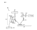
50 パターン転写装置
Claims (12)
- 基板上に、Mo膜とSi膜を1周期としてこれを複数周期積層させたMo/Siの交互積層膜からなる多層下地膜および露光光を反射する、Mo膜とSi膜を1周期としてこれを複数周期積層させたMo/Siの交互積層膜からなる多層反射膜を順次設けてなり、EUV光を露光光とするリソグラフィー法で使用される多層反射膜付き基板であって、前記多層下地膜の周期長をdbottom[単位:nm]、多層反射膜の周期長をdtop[単位:nm]とした場合、dbottom>dtopにおいて、式(1)
(n+0.15)×dtop≦dbottom≦(n+0.9)×dtop …(1)
(ただし、nは1以上の自然数である。)
の関係を満たすことを特徴とする多層反射膜付き基板。 - 基板上に、Mo膜とSi膜を1周期としてこれを複数周期積層させたMo/Siの交互積層膜からなる多層下地膜および露光光を反射する、Mo膜とSi膜を1周期としてこれを複数周期積層させたMo/Siの交互積層膜からなる多層反射膜を順次設けてなり、EUV光を露光光とするリソグラフィー法で使用される多層反射膜付き基板であって、前記多層下地膜の周期長をdbottom[単位:nm]、多層反射膜の周期長をdtop[単位:nm]とした場合、dbottom<dtopにおいて、式(2)
dbottom≦0.6×dtop …(2)
の関係を満たすことを特徴とする多層反射膜付き基板。 - 多層反射膜において、dtopが6.5〜7.5nmで、かつΓMo[見かけのMo層の厚さ/周期長]が0.25〜0.70である請求項1または2に記載の多層反射膜付き基板。
- 基板上に、Mo膜とSi膜を1周期としてこれを複数周期積層させたMo/Siの交互積層膜からなる多層下地膜、Si膜からなる中間層および露光光を反射する、Mo膜とSi膜を1周期としてこれを複数周期積層させたMo/Siの交互積層膜からなる多層反射膜を順次設けてなり、EUV光を露光光とするリソグラフィー法で使用される多層反射膜付き基板であって、
前記多層下地膜の周期長dbottomが8.0〜12.0nmであり、
前記多層反射膜の周期長dtopが6.5nm〜7.5nmであることを特徴とする多層反射膜付き基板。 - 多層反射膜におけるΓMo[見かけのMo層の厚さ/周期長]が0.25〜0.70である請求項4に記載の多層反射膜付き基板。
- 多層下地膜の周期数は、10〜80である請求項1から5のいずれかに記載の多層反射膜付き基板。
- 多層反射膜の周期数は、40〜70である請求項1から6のいずれかに記載の多層反射膜付き基板。
- 多層下地膜と多層反射膜との間に、ケイ素膜からなる中間層を介在させてなる請求項1〜7のいずれかに記載の多層反射膜付き基板。
- 基板上に、Mo膜とSi膜を1周期としてこれを複数周期積層させたMo/Siの交互積層膜からなる多層下地膜および露光光を反射する、Mo膜とSi膜を1周期としてこれを複数周期積層させたMo/Siの交互積層膜からなる多層反射膜を、順次成膜する方法であって、
前記多層下地膜の成膜は、前記基板に向ってターゲットからの飛散粒子が、実質上垂直な方向から入射する直入射成膜方式で複数周期の積層を行う工程と、前記基板に向ってターゲットからの飛散粒子が、垂直方向に対し斜め方向から入射する斜入射成膜方式で複数周期の積層を行う工程を組み合わせることにより行われることを特徴とする、請求項1〜8のいずれかに記載の多層反射膜付き基板の製造方法。 - 多層下地膜および多層反射膜の成膜をイオンビームスパッタリング法で行う請求項9に記載の多層反射膜付き基板の製造方法。
- 請求項1から8のいずれかに記載の多層反射膜付き基板における多層反射膜上に、露光光を吸収する吸収体膜を形成してなることを特徴とする反射型マスクブランク。
- 請求項11に記載の反射型マスクブランクにおける吸収体膜に、転写パターンとなる吸収体膜パターンを形成してなることを特徴とする反射型マスク。
Priority Applications (3)
| Application Number | Priority Date | Filing Date | Title |
|---|---|---|---|
| JP2005300556A JP4905914B2 (ja) | 2005-10-14 | 2005-10-14 | 多層反射膜付き基板、その製造方法、反射型マスクブランクおよび反射型マスク |
| KR1020060099352A KR101219470B1 (ko) | 2005-10-14 | 2006-10-12 | 다층 반사막 코팅 기판, 그 제조 방법, 반사형 마스크블랭크 및 반사형 마스크 |
| US11/580,934 US7804648B2 (en) | 2005-10-14 | 2006-10-16 | Multilayer reflective film coated substrate, manufacturing method thereof, reflective mask blank, and reflective mask |
Applications Claiming Priority (1)
| Application Number | Priority Date | Filing Date | Title |
|---|---|---|---|
| JP2005300556A JP4905914B2 (ja) | 2005-10-14 | 2005-10-14 | 多層反射膜付き基板、その製造方法、反射型マスクブランクおよび反射型マスク |
Publications (2)
| Publication Number | Publication Date |
|---|---|
| JP2007108516A JP2007108516A (ja) | 2007-04-26 |
| JP4905914B2 true JP4905914B2 (ja) | 2012-03-28 |
Family
ID=37985062
Family Applications (1)
| Application Number | Title | Priority Date | Filing Date |
|---|---|---|---|
| JP2005300556A Expired - Fee Related JP4905914B2 (ja) | 2005-10-14 | 2005-10-14 | 多層反射膜付き基板、その製造方法、反射型マスクブランクおよび反射型マスク |
Country Status (3)
| Country | Link |
|---|---|
| US (1) | US7804648B2 (ja) |
| JP (1) | JP4905914B2 (ja) |
| KR (1) | KR101219470B1 (ja) |
Cited By (1)
| Publication number | Priority date | Publication date | Assignee | Title |
|---|---|---|---|---|
| US9261773B2 (en) | 2013-02-20 | 2016-02-16 | Asahi Glass Company, Limited | Reflective mask blank for EUV lithography, and reflective layer-coated substrate for EUV lithography |
Families Citing this family (15)
| Publication number | Priority date | Publication date | Assignee | Title |
|---|---|---|---|---|
| JP4666365B2 (ja) * | 2005-10-14 | 2011-04-06 | Hoya株式会社 | 多層反射膜付き基板、その製造方法、反射型マスクブランクおよび反射型マスク |
| DE102008040964B4 (de) * | 2008-08-04 | 2010-07-15 | Carl Zeiss Smt Ag | Entfernen reflektierender Schichten von EUV-Spiegeln |
| DE102008042212A1 (de) | 2008-09-19 | 2010-04-01 | Carl Zeiss Smt Ag | Reflektives optisches Element und Verfahren zu seiner Herstellung |
| JP5372455B2 (ja) * | 2008-10-04 | 2013-12-18 | Hoya株式会社 | 反射型マスクブランク及び反射型マスク、並びにこれらの製造方法 |
| JP2010109336A (ja) * | 2008-10-04 | 2010-05-13 | Hoya Corp | 反射型マスクの製造方法 |
| DE102009032779A1 (de) * | 2009-07-10 | 2011-01-13 | Carl Zeiss Smt Ag | Spiegel für den EUV-Wellenlängenbereich, Projektionsobjektiv für die Mikrolithographie mit einem solchen Spiegel und Projektionsbelichtungsanlage für die Mikrolithographie mit einem solchen Projektionsobjektiv |
| DE102009029471A1 (de) * | 2009-09-15 | 2011-03-31 | Carl Zeiss Smt Gmbh | Spiegel zur Verwendung in einer Mikrolithographie-Projektionsbelichtungsanlage |
| DE102011005543A1 (de) * | 2011-03-15 | 2012-09-20 | Carl Zeiss Smt Gmbh | Verfahren zur Korrektur der Oberflächenform eines Spiegels |
| US9249501B2 (en) | 2011-05-18 | 2016-02-02 | Carl Zeiss Smt Gmbh | Surface correction on coated mirrors |
| JP5816499B2 (ja) * | 2011-09-12 | 2015-11-18 | ルネサスエレクトロニクス株式会社 | Euvマスクの製造方法 |
| DE102011085358B3 (de) * | 2011-10-28 | 2012-07-12 | Carl Zeiss Smt Gmbh | Optische Anordnung für die EUV-Lithographie und Verfahren zum Konfigurieren einer solchen optischen Anordnung |
| DE102013212462A1 (de) | 2013-06-27 | 2015-01-15 | Carl Zeiss Smt Gmbh | Oberflächenkorrektur von Spiegeln mit Entkopplungsbeschichtung |
| CN104575655A (zh) * | 2013-10-10 | 2015-04-29 | 同济大学 | 一种针对多个工作能点响应的x射线多层膜结构 |
| JP7447812B2 (ja) * | 2019-01-21 | 2024-03-12 | Agc株式会社 | 反射型マスクブランク、反射型マスク、および反射型マスクブランクの製造方法 |
| US12181797B2 (en) * | 2021-05-28 | 2024-12-31 | Taiwan Semiconductor Manufacturing Co., Ltd. | Extreme ultraviolet mask with alloy based absorbers |
Family Cites Families (12)
| Publication number | Priority date | Publication date | Assignee | Title |
|---|---|---|---|---|
| US5485497A (en) * | 1991-11-12 | 1996-01-16 | Hitachi, Ltd. | Optical element and projection exposure apparatus employing the same |
| JPH08213303A (ja) | 1995-02-03 | 1996-08-20 | Nikon Corp | 反射型x線マスク及びその製造法 |
| JPH11305417A (ja) * | 1998-04-24 | 1999-11-05 | Hitachi Ltd | 露光方法および反射型マスク |
| US6319635B1 (en) * | 1999-12-06 | 2001-11-20 | The Regents Of The University Of California | Mitigation of substrate defects in reticles using multilayer buffer layers |
| TW519574B (en) * | 2000-10-20 | 2003-02-01 | Nikon Corp | Multilayer mirror and method for making the same, and EUV optical system comprising the same, and EUV microlithography system comprising the same |
| JP2002313694A (ja) * | 2001-04-11 | 2002-10-25 | Nikon Corp | 反射マスク |
| JP4437290B2 (ja) * | 2003-05-14 | 2010-03-24 | シーワイジー技術研究所株式会社 | スパッタ装置 |
| JP4538254B2 (ja) * | 2004-03-25 | 2010-09-08 | ルネサスエレクトロニクス株式会社 | Euvリソグラフィー用マスク基板及びその製造方法 |
| US7522335B2 (en) * | 2004-03-29 | 2009-04-21 | Intel Corporation | Broad-angle multilayer mirror design |
| JP4532991B2 (ja) * | 2004-05-26 | 2010-08-25 | キヤノン株式会社 | 投影光学系、露光装置及びデバイス製造方法 |
| JP4834205B2 (ja) * | 2005-08-11 | 2011-12-14 | Hoya株式会社 | 多層反射膜付き基板の製造方法、反射型マスクブランクの製造方法、及び反射型マスクの製造方法 |
| JP4666365B2 (ja) * | 2005-10-14 | 2011-04-06 | Hoya株式会社 | 多層反射膜付き基板、その製造方法、反射型マスクブランクおよび反射型マスク |
-
2005
- 2005-10-14 JP JP2005300556A patent/JP4905914B2/ja not_active Expired - Fee Related
-
2006
- 2006-10-12 KR KR1020060099352A patent/KR101219470B1/ko active Active
- 2006-10-16 US US11/580,934 patent/US7804648B2/en not_active Expired - Fee Related
Cited By (1)
| Publication number | Priority date | Publication date | Assignee | Title |
|---|---|---|---|---|
| US9261773B2 (en) | 2013-02-20 | 2016-02-16 | Asahi Glass Company, Limited | Reflective mask blank for EUV lithography, and reflective layer-coated substrate for EUV lithography |
Also Published As
| Publication number | Publication date |
|---|---|
| KR101219470B1 (ko) | 2013-01-11 |
| JP2007108516A (ja) | 2007-04-26 |
| US7804648B2 (en) | 2010-09-28 |
| US20070091420A1 (en) | 2007-04-26 |
| KR20070041357A (ko) | 2007-04-18 |
Similar Documents
| Publication | Publication Date | Title |
|---|---|---|
| JP4666365B2 (ja) | 多層反射膜付き基板、その製造方法、反射型マスクブランクおよび反射型マスク | |
| US20230168575A1 (en) | Reflective mask blank, reflective mask and manufacturing method thereof, and semiconductor device manufacturing method | |
| JP4652946B2 (ja) | 反射型マスクブランク用基板の製造方法、反射型マスクブランクの製造方法、及び反射型マスクの製造方法 | |
| US8709685B2 (en) | Reflective mask blank and method of manufacturing a reflective mask | |
| JP4905914B2 (ja) | 多層反射膜付き基板、その製造方法、反射型マスクブランクおよび反射型マスク | |
| JP7635802B2 (ja) | Euvリソグラフィ用反射型マスクブランク | |
| JP4703354B2 (ja) | 多層反射膜付き基板、その製造方法、反射型マスクブランクおよび反射型マスク | |
| JP6377361B2 (ja) | 多層反射膜付き基板及びその製造方法、反射型マスクブランクの製造方法、反射型マスクの製造方法、並びに半導体装置の製造方法 | |
| JP2005210093A (ja) | 多層反射膜付き基板、露光用反射型マスクブランクス及び露光用反射型マスク、並びにそれらの製造方法 | |
| JP7612408B2 (ja) | 反射型マスクブランク、反射型マスク、反射型マスクの製造方法、及び半導体デバイスの製造方法 | |
| KR20160054458A (ko) | 다층 반사막을 구비한 기판, euv 리소그래피용 반사형 마스크 블랭크, euv 리소그래피용 반사형 마스크 및 그 제조 방법과 반도체 장치의 제조 방법 | |
| JP6441012B2 (ja) | 反射型マスクブランク、反射型マスク及びその製造方法、並びに半導体装置の製造方法 | |
| JP7722380B2 (ja) | 反射型マスク、反射型マスクブランク、および反射型マスクの製造方法 | |
| KR20140104375A (ko) | Euv 리소그래피용 반사형 마스크 블랭크 및 그 마스크 블랭크용 반사층 형성 기판 | |
| JP5258368B2 (ja) | 多層反射膜付基板の製造方法、反射型マスクブランクの製造方法、及び反射型マスクの製造方法 | |
| JP6855190B2 (ja) | 反射型マスク、並びに反射型マスクブランク及び半導体装置の製造方法 | |
| JP4703353B2 (ja) | 多層反射膜付き基板、その製造方法、反射型マスクブランクおよび反射型マスク | |
| JP7363913B2 (ja) | 反射型マスクブランクおよび反射型マスク | |
| JP4834205B2 (ja) | 多層反射膜付き基板の製造方法、反射型マスクブランクの製造方法、及び反射型マスクの製造方法 | |
| KR20250093487A (ko) | 반사형 마스크 블랭크 및 반사형 마스크, 그리고 반사형 마스크 및 반도체 장치의 제조 방법 | |
| JP5568158B2 (ja) | 多層反射膜付基板の製造方法、反射型マスクブランクの製造方法、及び反射型マスクの製造方法 | |
| JP4300930B2 (ja) | 極限紫外線露光用マスク及びブランク並びにパターン転写方法 | |
| TW202443289A (zh) | 反射型遮罩基底及反射型遮罩、以及反射型遮罩及半導體裝置之製造方法 | |
| WO2024176704A1 (ja) | 反射型マスクブランク、反射型マスク及び半導体デバイスの製造方法 | |
| WO2024029409A1 (ja) | 反射型マスクブランク及び反射型マスク |
Legal Events
| Date | Code | Title | Description |
|---|---|---|---|
| A621 | Written request for application examination |
Free format text: JAPANESE INTERMEDIATE CODE: A621 Effective date: 20071113 |
|
| A131 | Notification of reasons for refusal |
Free format text: JAPANESE INTERMEDIATE CODE: A131 Effective date: 20110105 |
|
| A521 | Request for written amendment filed |
Free format text: JAPANESE INTERMEDIATE CODE: A523 Effective date: 20110304 |
|
| TRDD | Decision of grant or rejection written | ||
| A01 | Written decision to grant a patent or to grant a registration (utility model) |
Free format text: JAPANESE INTERMEDIATE CODE: A01 Effective date: 20120105 |
|
| A01 | Written decision to grant a patent or to grant a registration (utility model) |
Free format text: JAPANESE INTERMEDIATE CODE: A01 |
|
| A61 | First payment of annual fees (during grant procedure) |
Free format text: JAPANESE INTERMEDIATE CODE: A61 Effective date: 20120105 |
|
| FPAY | Renewal fee payment (event date is renewal date of database) |
Free format text: PAYMENT UNTIL: 20150120 Year of fee payment: 3 |
|
| R150 | Certificate of patent or registration of utility model |
Free format text: JAPANESE INTERMEDIATE CODE: R150 |
|
| R250 | Receipt of annual fees |
Free format text: JAPANESE INTERMEDIATE CODE: R250 |
|
| R250 | Receipt of annual fees |
Free format text: JAPANESE INTERMEDIATE CODE: R250 |
|
| R250 | Receipt of annual fees |
Free format text: JAPANESE INTERMEDIATE CODE: R250 |
|
| LAPS | Cancellation because of no payment of annual fees |