JP4931348B2 - 半導体ナノクリスタルヘテロ構造体 - Google Patents
半導体ナノクリスタルヘテロ構造体 Download PDFInfo
- Publication number
- JP4931348B2 JP4931348B2 JP2004559043A JP2004559043A JP4931348B2 JP 4931348 B2 JP4931348 B2 JP 4931348B2 JP 2004559043 A JP2004559043 A JP 2004559043A JP 2004559043 A JP2004559043 A JP 2004559043A JP 4931348 B2 JP4931348 B2 JP 4931348B2
- Authority
- JP
- Japan
- Prior art keywords
- semiconductor material
- nanocrystal
- nanocrystals
- band
- core
- Prior art date
- Legal status (The legal status is an assumption and is not a legal conclusion. Google has not performed a legal analysis and makes no representation as to the accuracy of the status listed.)
- Expired - Lifetime
Links
Images



Classifications
-
- G—PHYSICS
- G01—MEASURING; TESTING
- G01N—INVESTIGATING OR ANALYSING MATERIALS BY DETERMINING THEIR CHEMICAL OR PHYSICAL PROPERTIES
- G01N33/00—Investigating or analysing materials by specific methods not covered by groups G01N1/00 - G01N31/00
- G01N33/48—Biological material, e.g. blood, urine; Haemocytometers
- G01N33/50—Chemical analysis of biological material, e.g. blood, urine; Testing involving biospecific ligand binding methods; Immunological testing
- G01N33/58—Chemical analysis of biological material, e.g. blood, urine; Testing involving biospecific ligand binding methods; Immunological testing involving labelled substances
- G01N33/588—Chemical analysis of biological material, e.g. blood, urine; Testing involving biospecific ligand binding methods; Immunological testing involving labelled substances with semiconductor nanocrystal label, e.g. quantum dots
-
- B—PERFORMING OPERATIONS; TRANSPORTING
- B82—NANOTECHNOLOGY
- B82Y—SPECIFIC USES OR APPLICATIONS OF NANOSTRUCTURES; MEASUREMENT OR ANALYSIS OF NANOSTRUCTURES; MANUFACTURE OR TREATMENT OF NANOSTRUCTURES
- B82Y10/00—Nanotechnology for information processing, storage or transmission, e.g. quantum computing or single electron logic
-
- B—PERFORMING OPERATIONS; TRANSPORTING
- B82—NANOTECHNOLOGY
- B82Y—SPECIFIC USES OR APPLICATIONS OF NANOSTRUCTURES; MEASUREMENT OR ANALYSIS OF NANOSTRUCTURES; MANUFACTURE OR TREATMENT OF NANOSTRUCTURES
- B82Y15/00—Nanotechnology for interacting, sensing or actuating, e.g. quantum dots as markers in protein assays or molecular motors
-
- B—PERFORMING OPERATIONS; TRANSPORTING
- B82—NANOTECHNOLOGY
- B82Y—SPECIFIC USES OR APPLICATIONS OF NANOSTRUCTURES; MEASUREMENT OR ANALYSIS OF NANOSTRUCTURES; MANUFACTURE OR TREATMENT OF NANOSTRUCTURES
- B82Y20/00—Nanooptics, e.g. quantum optics or photonic crystals
-
- B—PERFORMING OPERATIONS; TRANSPORTING
- B82—NANOTECHNOLOGY
- B82Y—SPECIFIC USES OR APPLICATIONS OF NANOSTRUCTURES; MEASUREMENT OR ANALYSIS OF NANOSTRUCTURES; MANUFACTURE OR TREATMENT OF NANOSTRUCTURES
- B82Y30/00—Nanotechnology for materials or surface science, e.g. nanocomposites
-
- C—CHEMISTRY; METALLURGY
- C09—DYES; PAINTS; POLISHES; NATURAL RESINS; ADHESIVES; COMPOSITIONS NOT OTHERWISE PROVIDED FOR; APPLICATIONS OF MATERIALS NOT OTHERWISE PROVIDED FOR
- C09K—MATERIALS FOR MISCELLANEOUS APPLICATIONS, NOT PROVIDED FOR ELSEWHERE
- C09K11/00—Luminescent materials, e.g. electroluminescent or chemiluminescent
- C09K11/08—Luminescent materials, e.g. electroluminescent or chemiluminescent containing inorganic luminescent materials
- C09K11/88—Luminescent materials, e.g. electroluminescent or chemiluminescent containing inorganic luminescent materials containing selenium, tellurium or unspecified chalcogen elements
- C09K11/881—Chalcogenides
- C09K11/883—Chalcogenides with zinc or cadmium
-
- C—CHEMISTRY; METALLURGY
- C30—CRYSTAL GROWTH
- C30B—SINGLE-CRYSTAL GROWTH; UNIDIRECTIONAL SOLIDIFICATION OF EUTECTIC MATERIAL OR UNIDIRECTIONAL DEMIXING OF EUTECTOID MATERIAL; REFINING BY ZONE-MELTING OF MATERIAL; PRODUCTION OF A HOMOGENEOUS POLYCRYSTALLINE MATERIAL WITH DEFINED STRUCTURE; SINGLE CRYSTALS OR HOMOGENEOUS POLYCRYSTALLINE MATERIAL WITH DEFINED STRUCTURE; AFTER-TREATMENT OF SINGLE CRYSTALS OR A HOMOGENEOUS POLYCRYSTALLINE MATERIAL WITH DEFINED STRUCTURE; APPARATUS THEREFOR
- C30B29/00—Single crystals or homogeneous polycrystalline material with defined structure characterised by the material or by their shape
- C30B29/60—Single crystals or homogeneous polycrystalline material with defined structure characterised by the material or by their shape characterised by shape
- C30B29/605—Products containing multiple oriented crystallites, e.g. columnar crystallites
-
- C—CHEMISTRY; METALLURGY
- C30—CRYSTAL GROWTH
- C30B—SINGLE-CRYSTAL GROWTH; UNIDIRECTIONAL SOLIDIFICATION OF EUTECTIC MATERIAL OR UNIDIRECTIONAL DEMIXING OF EUTECTOID MATERIAL; REFINING BY ZONE-MELTING OF MATERIAL; PRODUCTION OF A HOMOGENEOUS POLYCRYSTALLINE MATERIAL WITH DEFINED STRUCTURE; SINGLE CRYSTALS OR HOMOGENEOUS POLYCRYSTALLINE MATERIAL WITH DEFINED STRUCTURE; AFTER-TREATMENT OF SINGLE CRYSTALS OR A HOMOGENEOUS POLYCRYSTALLINE MATERIAL WITH DEFINED STRUCTURE; APPARATUS THEREFOR
- C30B33/00—After-treatment of single crystals or homogeneous polycrystalline material with defined structure
-
- C—CHEMISTRY; METALLURGY
- C30—CRYSTAL GROWTH
- C30B—SINGLE-CRYSTAL GROWTH; UNIDIRECTIONAL SOLIDIFICATION OF EUTECTIC MATERIAL OR UNIDIRECTIONAL DEMIXING OF EUTECTOID MATERIAL; REFINING BY ZONE-MELTING OF MATERIAL; PRODUCTION OF A HOMOGENEOUS POLYCRYSTALLINE MATERIAL WITH DEFINED STRUCTURE; SINGLE CRYSTALS OR HOMOGENEOUS POLYCRYSTALLINE MATERIAL WITH DEFINED STRUCTURE; AFTER-TREATMENT OF SINGLE CRYSTALS OR A HOMOGENEOUS POLYCRYSTALLINE MATERIAL WITH DEFINED STRUCTURE; APPARATUS THEREFOR
- C30B7/00—Single-crystal growth from solutions using solvents which are liquid at normal temperature, e.g. aqueous solutions
-
- H—ELECTRICITY
- H10—SEMICONDUCTOR DEVICES; ELECTRIC SOLID-STATE DEVICES NOT OTHERWISE PROVIDED FOR
- H10D—INORGANIC ELECTRIC SEMICONDUCTOR DEVICES
- H10D62/00—Semiconductor bodies, or regions thereof, of devices having potential barriers
- H10D62/10—Shapes, relative sizes or dispositions of the regions of the semiconductor bodies; Shapes of the semiconductor bodies
- H10D62/117—Shapes of semiconductor bodies
- H10D62/118—Nanostructure semiconductor bodies
-
- H—ELECTRICITY
- H10—SEMICONDUCTOR DEVICES; ELECTRIC SOLID-STATE DEVICES NOT OTHERWISE PROVIDED FOR
- H10D—INORGANIC ELECTRIC SEMICONDUCTOR DEVICES
- H10D62/00—Semiconductor bodies, or regions thereof, of devices having potential barriers
- H10D62/10—Shapes, relative sizes or dispositions of the regions of the semiconductor bodies; Shapes of the semiconductor bodies
- H10D62/117—Shapes of semiconductor bodies
- H10D62/118—Nanostructure semiconductor bodies
- H10D62/119—Nanowire, nanosheet or nanotube semiconductor bodies
- H10D62/121—Nanowire, nanosheet or nanotube semiconductor bodies oriented parallel to substrates
-
- H—ELECTRICITY
- H10—SEMICONDUCTOR DEVICES; ELECTRIC SOLID-STATE DEVICES NOT OTHERWISE PROVIDED FOR
- H10D—INORGANIC ELECTRIC SEMICONDUCTOR DEVICES
- H10D62/00—Semiconductor bodies, or regions thereof, of devices having potential barriers
- H10D62/80—Semiconductor bodies, or regions thereof, of devices having potential barriers characterised by the materials
- H10D62/82—Heterojunctions
-
- H—ELECTRICITY
- H10—SEMICONDUCTOR DEVICES; ELECTRIC SOLID-STATE DEVICES NOT OTHERWISE PROVIDED FOR
- H10D—INORGANIC ELECTRIC SEMICONDUCTOR DEVICES
- H10D62/00—Semiconductor bodies, or regions thereof, of devices having potential barriers
- H10D62/80—Semiconductor bodies, or regions thereof, of devices having potential barriers characterised by the materials
- H10D62/82—Heterojunctions
- H10D62/822—Heterojunctions comprising only Group IV materials heterojunctions, e.g. Si/Ge heterojunctions
-
- H—ELECTRICITY
- H10—SEMICONDUCTOR DEVICES; ELECTRIC SOLID-STATE DEVICES NOT OTHERWISE PROVIDED FOR
- H10D—INORGANIC ELECTRIC SEMICONDUCTOR DEVICES
- H10D62/00—Semiconductor bodies, or regions thereof, of devices having potential barriers
- H10D62/80—Semiconductor bodies, or regions thereof, of devices having potential barriers characterised by the materials
- H10D62/82—Heterojunctions
- H10D62/824—Heterojunctions comprising only Group III-V materials heterojunctions, e.g. GaN/AlGaN heterojunctions
-
- H—ELECTRICITY
- H10—SEMICONDUCTOR DEVICES; ELECTRIC SOLID-STATE DEVICES NOT OTHERWISE PROVIDED FOR
- H10D—INORGANIC ELECTRIC SEMICONDUCTOR DEVICES
- H10D62/00—Semiconductor bodies, or regions thereof, of devices having potential barriers
- H10D62/80—Semiconductor bodies, or regions thereof, of devices having potential barriers characterised by the materials
- H10D62/82—Heterojunctions
- H10D62/826—Heterojunctions comprising only Group II-VI materials heterojunctions, e.g. CdTe/HgTe heterojunctions
-
- H—ELECTRICITY
- H10—SEMICONDUCTOR DEVICES; ELECTRIC SOLID-STATE DEVICES NOT OTHERWISE PROVIDED FOR
- H10P—GENERIC PROCESSES OR APPARATUS FOR THE MANUFACTURE OR TREATMENT OF DEVICES COVERED BY CLASS H10
- H10P14/00—Formation of materials, e.g. in the shape of layers or pillars
- H10P14/20—Formation of materials, e.g. in the shape of layers or pillars of semiconductor materials
- H10P14/29—Formation of materials, e.g. in the shape of layers or pillars of semiconductor materials characterised by the substrates
- H10P14/2901—Materials
-
- H—ELECTRICITY
- H10—SEMICONDUCTOR DEVICES; ELECTRIC SOLID-STATE DEVICES NOT OTHERWISE PROVIDED FOR
- H10P—GENERIC PROCESSES OR APPARATUS FOR THE MANUFACTURE OR TREATMENT OF DEVICES COVERED BY CLASS H10
- H10P14/00—Formation of materials, e.g. in the shape of layers or pillars
- H10P14/20—Formation of materials, e.g. in the shape of layers or pillars of semiconductor materials
- H10P14/29—Formation of materials, e.g. in the shape of layers or pillars of semiconductor materials characterised by the substrates
- H10P14/2901—Materials
- H10P14/2913—Materials being Group IIB-VIA materials
- H10P14/2916—Selenides
-
- H—ELECTRICITY
- H10—SEMICONDUCTOR DEVICES; ELECTRIC SOLID-STATE DEVICES NOT OTHERWISE PROVIDED FOR
- H10P—GENERIC PROCESSES OR APPARATUS FOR THE MANUFACTURE OR TREATMENT OF DEVICES COVERED BY CLASS H10
- H10P14/00—Formation of materials, e.g. in the shape of layers or pillars
- H10P14/20—Formation of materials, e.g. in the shape of layers or pillars of semiconductor materials
- H10P14/29—Formation of materials, e.g. in the shape of layers or pillars of semiconductor materials characterised by the substrates
- H10P14/2901—Materials
- H10P14/2913—Materials being Group IIB-VIA materials
- H10P14/2917—Tellurides
-
- H—ELECTRICITY
- H10—SEMICONDUCTOR DEVICES; ELECTRIC SOLID-STATE DEVICES NOT OTHERWISE PROVIDED FOR
- H10P—GENERIC PROCESSES OR APPARATUS FOR THE MANUFACTURE OR TREATMENT OF DEVICES COVERED BY CLASS H10
- H10P14/00—Formation of materials, e.g. in the shape of layers or pillars
- H10P14/20—Formation of materials, e.g. in the shape of layers or pillars of semiconductor materials
- H10P14/34—Deposited materials, e.g. layers
- H10P14/3402—Deposited materials, e.g. layers characterised by the chemical composition
-
- H—ELECTRICITY
- H10—SEMICONDUCTOR DEVICES; ELECTRIC SOLID-STATE DEVICES NOT OTHERWISE PROVIDED FOR
- H10P—GENERIC PROCESSES OR APPARATUS FOR THE MANUFACTURE OR TREATMENT OF DEVICES COVERED BY CLASS H10
- H10P14/00—Formation of materials, e.g. in the shape of layers or pillars
- H10P14/20—Formation of materials, e.g. in the shape of layers or pillars of semiconductor materials
- H10P14/34—Deposited materials, e.g. layers
- H10P14/3402—Deposited materials, e.g. layers characterised by the chemical composition
- H10P14/3424—Deposited materials, e.g. layers characterised by the chemical composition being Group IIB-VIA materials
- H10P14/3431—Selenides
-
- H—ELECTRICITY
- H10—SEMICONDUCTOR DEVICES; ELECTRIC SOLID-STATE DEVICES NOT OTHERWISE PROVIDED FOR
- H10P—GENERIC PROCESSES OR APPARATUS FOR THE MANUFACTURE OR TREATMENT OF DEVICES COVERED BY CLASS H10
- H10P14/00—Formation of materials, e.g. in the shape of layers or pillars
- H10P14/20—Formation of materials, e.g. in the shape of layers or pillars of semiconductor materials
- H10P14/34—Deposited materials, e.g. layers
- H10P14/3402—Deposited materials, e.g. layers characterised by the chemical composition
- H10P14/3424—Deposited materials, e.g. layers characterised by the chemical composition being Group IIB-VIA materials
- H10P14/3432—Tellurides
-
- H—ELECTRICITY
- H10—SEMICONDUCTOR DEVICES; ELECTRIC SOLID-STATE DEVICES NOT OTHERWISE PROVIDED FOR
- H10P—GENERIC PROCESSES OR APPARATUS FOR THE MANUFACTURE OR TREATMENT OF DEVICES COVERED BY CLASS H10
- H10P14/00—Formation of materials, e.g. in the shape of layers or pillars
- H10P14/20—Formation of materials, e.g. in the shape of layers or pillars of semiconductor materials
- H10P14/34—Deposited materials, e.g. layers
- H10P14/3451—Structure
- H10P14/3452—Microstructure
- H10P14/3461—Nanoparticles
-
- Y—GENERAL TAGGING OF NEW TECHNOLOGICAL DEVELOPMENTS; GENERAL TAGGING OF CROSS-SECTIONAL TECHNOLOGIES SPANNING OVER SEVERAL SECTIONS OF THE IPC; TECHNICAL SUBJECTS COVERED BY FORMER USPC CROSS-REFERENCE ART COLLECTIONS [XRACs] AND DIGESTS
- Y02—TECHNOLOGIES OR APPLICATIONS FOR MITIGATION OR ADAPTATION AGAINST CLIMATE CHANGE
- Y02E—REDUCTION OF GREENHOUSE GAS [GHG] EMISSIONS, RELATED TO ENERGY GENERATION, TRANSMISSION OR DISTRIBUTION
- Y02E10/00—Energy generation through renewable energy sources
- Y02E10/50—Photovoltaic [PV] energy
- Y02E10/549—Organic PV cells
-
- Y—GENERAL TAGGING OF NEW TECHNOLOGICAL DEVELOPMENTS; GENERAL TAGGING OF CROSS-SECTIONAL TECHNOLOGIES SPANNING OVER SEVERAL SECTIONS OF THE IPC; TECHNICAL SUBJECTS COVERED BY FORMER USPC CROSS-REFERENCE ART COLLECTIONS [XRACs] AND DIGESTS
- Y10—TECHNICAL SUBJECTS COVERED BY FORMER USPC
- Y10S—TECHNICAL SUBJECTS COVERED BY FORMER USPC CROSS-REFERENCE ART COLLECTIONS [XRACs] AND DIGESTS
- Y10S977/00—Nanotechnology
- Y10S977/70—Nanostructure
- Y10S977/773—Nanoparticle, i.e. structure having three dimensions of 100 nm or less
-
- Y—GENERAL TAGGING OF NEW TECHNOLOGICAL DEVELOPMENTS; GENERAL TAGGING OF CROSS-SECTIONAL TECHNOLOGIES SPANNING OVER SEVERAL SECTIONS OF THE IPC; TECHNICAL SUBJECTS COVERED BY FORMER USPC CROSS-REFERENCE ART COLLECTIONS [XRACs] AND DIGESTS
- Y10—TECHNICAL SUBJECTS COVERED BY FORMER USPC
- Y10S—TECHNICAL SUBJECTS COVERED BY FORMER USPC CROSS-REFERENCE ART COLLECTIONS [XRACs] AND DIGESTS
- Y10S977/00—Nanotechnology
- Y10S977/70—Nanostructure
- Y10S977/773—Nanoparticle, i.e. structure having three dimensions of 100 nm or less
- Y10S977/774—Exhibiting three-dimensional carrier confinement, e.g. quantum dots
-
- Y—GENERAL TAGGING OF NEW TECHNOLOGICAL DEVELOPMENTS; GENERAL TAGGING OF CROSS-SECTIONAL TECHNOLOGIES SPANNING OVER SEVERAL SECTIONS OF THE IPC; TECHNICAL SUBJECTS COVERED BY FORMER USPC CROSS-REFERENCE ART COLLECTIONS [XRACs] AND DIGESTS
- Y10—TECHNICAL SUBJECTS COVERED BY FORMER USPC
- Y10S—TECHNICAL SUBJECTS COVERED BY FORMER USPC CROSS-REFERENCE ART COLLECTIONS [XRACs] AND DIGESTS
- Y10S977/00—Nanotechnology
- Y10S977/70—Nanostructure
- Y10S977/773—Nanoparticle, i.e. structure having three dimensions of 100 nm or less
- Y10S977/775—Nanosized powder or flake, e.g. nanosized catalyst
- Y10S977/777—Metallic powder or flake
-
- Y—GENERAL TAGGING OF NEW TECHNOLOGICAL DEVELOPMENTS; GENERAL TAGGING OF CROSS-SECTIONAL TECHNOLOGIES SPANNING OVER SEVERAL SECTIONS OF THE IPC; TECHNICAL SUBJECTS COVERED BY FORMER USPC CROSS-REFERENCE ART COLLECTIONS [XRACs] AND DIGESTS
- Y10—TECHNICAL SUBJECTS COVERED BY FORMER USPC
- Y10S—TECHNICAL SUBJECTS COVERED BY FORMER USPC CROSS-REFERENCE ART COLLECTIONS [XRACs] AND DIGESTS
- Y10S977/00—Nanotechnology
- Y10S977/70—Nanostructure
- Y10S977/811—Of specified metal oxide composition, e.g. conducting or semiconducting compositions such as ITO, ZnOx
-
- Y—GENERAL TAGGING OF NEW TECHNOLOGICAL DEVELOPMENTS; GENERAL TAGGING OF CROSS-SECTIONAL TECHNOLOGIES SPANNING OVER SEVERAL SECTIONS OF THE IPC; TECHNICAL SUBJECTS COVERED BY FORMER USPC CROSS-REFERENCE ART COLLECTIONS [XRACs] AND DIGESTS
- Y10—TECHNICAL SUBJECTS COVERED BY FORMER USPC
- Y10T—TECHNICAL SUBJECTS COVERED BY FORMER US CLASSIFICATION
- Y10T428/00—Stock material or miscellaneous articles
- Y10T428/12—All metal or with adjacent metals
- Y10T428/12014—All metal or with adjacent metals having metal particles
- Y10T428/12021—All metal or with adjacent metals having metal particles having composition or density gradient or differential porosity
-
- Y—GENERAL TAGGING OF NEW TECHNOLOGICAL DEVELOPMENTS; GENERAL TAGGING OF CROSS-SECTIONAL TECHNOLOGIES SPANNING OVER SEVERAL SECTIONS OF THE IPC; TECHNICAL SUBJECTS COVERED BY FORMER USPC CROSS-REFERENCE ART COLLECTIONS [XRACs] AND DIGESTS
- Y10—TECHNICAL SUBJECTS COVERED BY FORMER USPC
- Y10T—TECHNICAL SUBJECTS COVERED BY FORMER US CLASSIFICATION
- Y10T428/00—Stock material or miscellaneous articles
- Y10T428/12—All metal or with adjacent metals
- Y10T428/12493—Composite; i.e., plural, adjacent, spatially distinct metal components [e.g., layers, joint, etc.]
- Y10T428/12528—Semiconductor component
-
- Y—GENERAL TAGGING OF NEW TECHNOLOGICAL DEVELOPMENTS; GENERAL TAGGING OF CROSS-SECTIONAL TECHNOLOGIES SPANNING OVER SEVERAL SECTIONS OF THE IPC; TECHNICAL SUBJECTS COVERED BY FORMER USPC CROSS-REFERENCE ART COLLECTIONS [XRACs] AND DIGESTS
- Y10—TECHNICAL SUBJECTS COVERED BY FORMER USPC
- Y10T—TECHNICAL SUBJECTS COVERED BY FORMER US CLASSIFICATION
- Y10T428/00—Stock material or miscellaneous articles
- Y10T428/12—All metal or with adjacent metals
- Y10T428/12493—Composite; i.e., plural, adjacent, spatially distinct metal components [e.g., layers, joint, etc.]
- Y10T428/12986—Adjacent functionally defined components
-
- Y—GENERAL TAGGING OF NEW TECHNOLOGICAL DEVELOPMENTS; GENERAL TAGGING OF CROSS-SECTIONAL TECHNOLOGIES SPANNING OVER SEVERAL SECTIONS OF THE IPC; TECHNICAL SUBJECTS COVERED BY FORMER USPC CROSS-REFERENCE ART COLLECTIONS [XRACs] AND DIGESTS
- Y10—TECHNICAL SUBJECTS COVERED BY FORMER USPC
- Y10T—TECHNICAL SUBJECTS COVERED BY FORMER US CLASSIFICATION
- Y10T428/00—Stock material or miscellaneous articles
- Y10T428/29—Coated or structually defined flake, particle, cell, strand, strand portion, rod, filament, macroscopic fiber or mass thereof
- Y10T428/2913—Rod, strand, filament or fiber
- Y10T428/2933—Coated or with bond, impregnation or core
- Y10T428/294—Coated or with bond, impregnation or core including metal or compound thereof [excluding glass, ceramic and asbestos]
-
- Y—GENERAL TAGGING OF NEW TECHNOLOGICAL DEVELOPMENTS; GENERAL TAGGING OF CROSS-SECTIONAL TECHNOLOGIES SPANNING OVER SEVERAL SECTIONS OF THE IPC; TECHNICAL SUBJECTS COVERED BY FORMER USPC CROSS-REFERENCE ART COLLECTIONS [XRACs] AND DIGESTS
- Y10—TECHNICAL SUBJECTS COVERED BY FORMER USPC
- Y10T—TECHNICAL SUBJECTS COVERED BY FORMER US CLASSIFICATION
- Y10T428/00—Stock material or miscellaneous articles
- Y10T428/29—Coated or structually defined flake, particle, cell, strand, strand portion, rod, filament, macroscopic fiber or mass thereof
- Y10T428/2982—Particulate matter [e.g., sphere, flake, etc.]
- Y10T428/2991—Coated
-
- Y—GENERAL TAGGING OF NEW TECHNOLOGICAL DEVELOPMENTS; GENERAL TAGGING OF CROSS-SECTIONAL TECHNOLOGIES SPANNING OVER SEVERAL SECTIONS OF THE IPC; TECHNICAL SUBJECTS COVERED BY FORMER USPC CROSS-REFERENCE ART COLLECTIONS [XRACs] AND DIGESTS
- Y10—TECHNICAL SUBJECTS COVERED BY FORMER USPC
- Y10T—TECHNICAL SUBJECTS COVERED BY FORMER US CLASSIFICATION
- Y10T428/00—Stock material or miscellaneous articles
- Y10T428/31—Surface property or characteristic of web, sheet or block
- Y10T428/315—Surface modified glass [e.g., tempered, strengthened, etc.]
Landscapes
- Chemical & Material Sciences (AREA)
- Engineering & Computer Science (AREA)
- Nanotechnology (AREA)
- Crystallography & Structural Chemistry (AREA)
- Materials Engineering (AREA)
- Life Sciences & Earth Sciences (AREA)
- Health & Medical Sciences (AREA)
- Physics & Mathematics (AREA)
- Organic Chemistry (AREA)
- Molecular Biology (AREA)
- Metallurgy (AREA)
- Biomedical Technology (AREA)
- General Health & Medical Sciences (AREA)
- Urology & Nephrology (AREA)
- Immunology (AREA)
- General Physics & Mathematics (AREA)
- Hematology (AREA)
- Optics & Photonics (AREA)
- Medicinal Chemistry (AREA)
- Theoretical Computer Science (AREA)
- Biophysics (AREA)
- Biotechnology (AREA)
- Cell Biology (AREA)
- Inorganic Chemistry (AREA)
- Condensed Matter Physics & Semiconductors (AREA)
- Microbiology (AREA)
- Composite Materials (AREA)
- Food Science & Technology (AREA)
- Mathematical Physics (AREA)
- Analytical Chemistry (AREA)
- Biochemistry (AREA)
- Pathology (AREA)
- Luminescent Compositions (AREA)
- Recrystallisation Techniques (AREA)
- Crystals, And After-Treatments Of Crystals (AREA)
- Physical Deposition Of Substances That Are Components Of Semiconductor Devices (AREA)
- Plural Heterocyclic Compounds (AREA)
- Heterocyclic Carbon Compounds Containing A Hetero Ring Having Oxygen Or Sulfur (AREA)
- Semiconductor Memories (AREA)
- Liquid Deposition Of Substances Of Which Semiconductor Devices Are Composed (AREA)
Description
本発明は、半導体ナノクリスタルヘテロ構造体に関するものである。
(連邦政府委託研究、または開発)
米国政府は、海軍研究事務所により授与された契約N00014-01-1-0787号に従う本発明において、特定の権利を有することができる。
半導体ナノクリスタルは、非常に興味のある対象となっており、ディスプレイデバイス、情報記憶、生物学的タグ材料、光電池、センサー、及び触媒を含む、有望で、広範囲の応用が見込まれている。小さい直径を有するナノクリスタルは、分子と物質のバルク形態との間の中間的な属性を有し得る。例えば、小さい直径を有する半導体物質を基礎とするナノクリスタルは、3次元すべてにおいて、該電子及び正孔、双方の量子閉じ込めを示すことができ、微結晶サイズの減少とともに、該物質の有効バンドギャップを増加させる。その結果、該微結晶のサイズ減少に伴い、ナノクリスタルの光吸収、及び発光の双方は、青(すなわち、高エネルギー)にシフトする。
一般に、半導体ナノクリスタルヘテロ構造体は、第二半導体物質のオーバーコーティングにより囲まれた第一半導体物質のコアを有する。該第一半導体物質、及び該第二半導体物質は、励起時に、一のキャリアが該コアに実質的に閉じ込められ、かつ他のキャリアが該オーバーコーティング層に実質的に閉じ込められるように選択される。一例において、該第一半導体物質の伝導帯は、該第二半導体物質の伝導帯よりも高エネルギーであり、かつ該第一半導体物質の価電子帯は、該第二半導体物質の価電子帯よりも高エネルギーである。他の例において、該第一半導体物質の伝導帯は、該第二半導体物質の伝導帯よりも低エネルギーであり、かつ該第一半導体物質の価電子帯は、該第二半導体物質の価電子帯よりも低エネルギーである。これらのバンド配置は、励起時に、エネルギー的に好ましい、キャリア(すなわち、該正孔と該電子)の空間的分離を創る。これらの構造は、II型へテロ構造である。対照的に、該第二半導体物質の伝導帯が、該第一半導体物質の伝導帯よりも高エネルギーであり、かつ該第二半導体物質の価電子帯が、該第一半導体物質の価電子帯よりも低エネルギーである構造は、I型ヘテロ構造である。I型へテロ構造のナノクリスタルは、該コア内に正孔と電子、双方の閉じ込めに有利である。I型、及びII型の用語は、量子井戸の文献から借用したもので、このような構造は、広く研究されている。
該ナノクリスタルは、励起時に、光を発することができ、最大発光強度の波長は、700 nmよりも長波長であり、又は700 nmから1500 nmの間である。該ナノクリスタルは、10%よりも大きい量子効率を有することができる。
本発明の他の特徴、目的、及び利点は、本説明と図面から、及び請求項から明らかになるであろう。
ナノクリスタルのコロイド合成法を、コアとオーバーコーティングと(コア-シェル)の構造を有し、かつII型へテロ構造を有するナノクリスタルの製造に使用することができる。コロイド合成法は、例えばMurray, C. B.らの論文(J. Am. Chem. Soc. 1993、115、8706)、Peng, X.らの論文(J Am. Chem. Soc. 1997、119、7019)、Dabbousi, B. O.らの論文(J. Phys. Chem. B 1997、101、9463)、及びCao, Y. W.とBanin, U.の論文(Angew. Chem. Int. Edit. 1999、38、3692)に記述されており、各論文は、その全体を引用により取り込まれている。該コロイド合成手段は、II-VI族、及びIII-V族の半導体物質すべてに適用することができる。
II型へテロ構造を有する半導体ナノクリスタルの例を、図1に示す。II型へテロ構造を有するナノクリスタルの励起時に、該キャリアは、一の半導体物質内に閉じ込められない。II型へテロ構造を有するナノクリスタルは、第二半導体のシェルにより囲まれた、一の半導体のコアナノクリスタルを含む。一のキャリアは、該コアに閉じ込めることができ、一方、他のキャリアは、ほとんど該シェルに閉じ込めることができる。図1に図示するように、該キャリアの相対的位置は、該コア、及び該シェルの物質に依存し得る。該二つの半導体物質のバンドオフセットは、エネルギー的に有利な、該正孔、及び該電子の空間的分離を作ることができる。II型へテロ構造を有するナノクリスタルは、I型へテロ構造を有するナノクリスタルでは生じない、キャリアの空間的分離のため、新たな特性を有することができる。他には、II型構造を有するナノクリスタルは、該ナノクリスタルを形成する半導体では、利用できないであろう発光波長(すなわち、最大発光強度の波長)を利用することができる。
ナノクリスタルの集団は、狭いサイズ分布を有することができる。該集団を単分散性とすることができ、かつ該ナノクリスタル直径の15%rms未満の偏差、好ましくは、10%未満、さらに好ましくは5%未満を示すことができる。最大強度の半値における全幅値(半値全幅)(FWHM)が10から150 nmの狭い範囲のスペクトル発光を観測することができる。II型構造を有する半導体ナノクリスタルは、2%、5%、10%、20%、40%、60%、70%、又は80%より大きい発光量子効率を有することができる。
該反応の成長段階の間のサイズ分布は、該粒子の吸収線幅をモニタリングすることによって評価することができる。該粒子の吸収スペクトルの変化に応答する反応温度の改質により、成長の間、鋭い粒子サイズ分布の維持が可能になる。反応物を、結晶成長の間、該核形成溶液に添加し、より大きな結晶に成長させることができる。特定のナノクリスタルの平均直径で、成長を停止し、平均して150Å未満のナノクリスタル直径を有する集団を得ることができる。ナノクリスタルの集団は、15Å〜125Åの範囲の平均直径を有することができる。
ビス-(トリメチルシリル)セレニドを、次のように調製した。スーパーヒドリド(superhydride)の溶液200 mL(Aldrich社製、テトラヒドロフラン中、水素化トリエチルホウ素リチウムの1.0 M溶液)に、Se塊7.89 g(Strem社製、99.99%)を加え、かつ室温で2時間攪拌した。クロロトリメチルシラン(25.2 g、Aldrich社製、99%)を、導入し、かつさらに、2〜3時間攪拌した。溶媒を、真空中で取り除いた。該生成物を、減圧蒸留により得た。
CdTe/CdSe(コア/シェル)ナノクリスタルの集団を、次のように調製した。沈殿したCdTeナノクリスタルを、トリオクチルホスフィンオキシド(TOPO、Alfa社製、95%)中に分散し、かつ減圧下160℃で乾燥した。トリオクチルホスフィン(TOP、Fluka社製、90%)中に、化学量論で1:1モル濃度のジメチルカドミウム(Strem社製、97%)とビス(トリメチルシリル)セレニドとを所望量混合することにより、オーバーコーティング原液を調製した。該CdTe-TOPO混合物を、Arフロー下で強く攪拌しながら、調製したオーバーコーティング原液を、ゆっくりと滴下して加えた。温度を、使用するCdTeナノクリスタルサイズに依存する、130℃から180℃の効果範囲に設定した。高温は、大きなサイズのCdTeナノクリスタルに必要である。
通常、CdSe/ZnTe(コア/シェル)ナノクリスタル集団を、CdTe/CdSeナノクリスタル用に記述された方法により調製した。ジエチル亜鉛(Strem社製、99.99%)とTOPTeとを、該前駆体として使用した。TOPTeは、室温下、TOP中にTe粉末(Strem社製、99.999%)を溶解することにより作った。
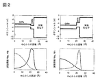
図3は、コアCdTe、及びCdSeナノクリスタル、及びII型構造を有する、CdTe/CdSe(コア/シェル)、及びCdSe/ZnTe(コア/シェル)ナノクリスタルの吸収と発光スペクトルとを示す。該左図は、半径32ÅのCdTeナノクリスタル(点線)、及びCdTe/CdSe(コア半径32Å/シェル厚さ11Å)ナノクリスタルのスペクトルを示す。該右図は、半径22ÅのCdSeナノクリスタル(点線)、及びCdSe/ZnTe(コア半径22Å/シェル厚さ18Å)ナノクリスタルのスペクトルを示す。該ナノクリスタルを、533 nmで励起することにより、該光ルミネッセンススペクトルを得た。該シェル成長前後の該ナノクリスタル振動子強度の総和の変化を、比較することができる。その理由は、これらは、該ナノクリスタルの空間的に積分した吸収率に比例するためである。該II型の発光は、該コアナノクリスタルのディープトラップ発光と関連していない。図3において、裸CdSeナノクリスタルのディープトラップ発光を、750 nm辺りに見い出すことができ、II型構造を有する、該対応するCdSe/ZnTe(コア/シェル)ナノクリスタルの発光波長とは一致しない。このことは、該ディープトラップ発光が残存する場合、シェル層の付着が、該コアのバンド端の発光を、単に消光するという可能性を排除している。
他の実施態様は、請求項の範囲内である。
Claims (13)
- 被覆されたナノクリスタルであって:
第一半導体物質を含むコアナノクリスタル;
該コアクリスタル上に第二半導体物質を含むオーバーコート;及び
被覆された該ナノクリスタルの表面上の有機層を含み、
該第一半導体物質、及び該第二半導体物質は、該ナノクリスタルが励起子を形成する励起時に、該励起子の一の電荷キャリアは該コアに実質的に閉じ込められ、かつ励起子の他の電荷キャリアは該オーバーコート層に実質的に閉じ込められるように選択され、
該第一半導体物質の伝導帯が該第二半導体物質の伝導帯よりも高いエネルギーであり、かつ該第一半導体物質の価電子帯が該第二半導体物質の価電子帯よりも高いエネルギーであり、
該第二半導体物質の伝導帯が、エネルギーにおいて、該第一半導体物質の価電子帯と伝導帯との中間にあるか;又は
該第一半導体物質の伝導帯が該第二半導体物質の伝導帯よりも低いエネルギーであり、かつ該第一半導体物質の価電子帯が該第二半導体物質の価電子帯よりも低いエネルギーであり、
該第二半導体物質の価電子帯が、エネルギーにおいて、該第一半導体物質の価電子帯と伝導帯との中間にある、
前記被覆されたナノクリスタル。 - CdTeを含む該第一半導体物質の伝導帯が、CdSeを含む該第二半導体物質の伝導帯よりも高いエネルギーであり、かつCdTeを含む該第一半導体物質の価電子帯が、CdSeを含む該第二半導体物質の価電子帯よりも高いエネルギーであるか;又は
CdSeを含む該第一半導体物質の伝導帯が、ZnTeを含む該第二半導体物質の伝導帯よりも低いエネルギーであり、かつCdSeを含む該第一半導体物質の価電子帯が、ZnTeを含む該第二半導体物質の価電子帯よりも低いエネルギーである、請求項1記載のナノクリスタル。 - 該ナノクリスタルが、励起時に光を発し、その最大発光強度の波長が、700nmより長波である、請求項1又は2記載のナノクリスタル。
- 該ナノクリスタルが、励起時に光を発し、その最大発光強度の波長が、700nmから1500nmの間である、請求項1から3のいずれか一項記載のナノクリスタル。
- 複数個のナノクリスタルが単分散性である、請求項1から4のいずれか一項記載の複数のナノクリスタルで構成された、該被覆ナノクリスタルの集団。
- 該第一被覆層上に第三半導体物質を含む、第二被膜層を更に有する、請求項1から4のいずれか一項記載のナノクリスタル。
- 量子効率が10%より大きい、請求項1から4及び6のいずれか一項記載のナノクリスタル。
- 請求項1から4、6及び7のいずれか一項記載の被覆されたナノクリスタルの製造方法であって:
第一半導体物質を含むコアナノクリスタルをオーバーコーティング反応混合物へ投入すること;及び
該コアナノクリスタル上の第二半導体物質をオーバーコーティングすることを含み、
該第一半導体物質、及び該第二半導体物質は、該ナノクリスタルが励起子を形成する励起時に、該励起子の一の電荷キャリアは該コアに実質的に閉じ込められ、かつ該励起子の他の電荷キャリアは該オーバーコート層に実質的に閉じ込められるように選択され、
該第一半導体物質の伝導帯が該第二半導体物質の伝導帯よりも高いエネルギーであり、かつ該第一半導体物質の価電子帯が該第二半導体物質の価電子帯よりも高いエネルギーであり、
該第二半導体物質の伝導帯が、エネルギーにおいて、該第一半導体物質の価電子帯と伝導帯との中間にあるか;又は
該第一半導体物質の伝導帯が該第二半導体物質の伝導帯よりも低いエネルギーであり、かつ該第一半導体物質の価電子帯が該第二半導体物質の価電子帯よりも低いエネルギーであり、
該第二半導体物質の価電子帯が、エネルギーにおいて、該第一半導体物質の価電子帯と伝導帯との中間にある、
前記製造方法。 - 該ナノクリスタルを、該被覆ナノクリスタルの表面への親和性を有する有機化合物へ曝露することを更に含む、請求項8記載の製造方法。
- 該被覆ナノクリスタルが液体中において分散性を有する、請求項8又は9記載の製造方法。
- 該第二半導体物質上に第三半導体物質をオーバーコートすることを更に含む、請求項8から10のいずれか一項記載の製造方法。
- 該第三半導体物質が、該第二半導体物質と比較して、不整合なバンドオフセットを有する、請求項11記載の製造方法。
- CdTeを含む該第一半導体物質の伝導帯が、CdSeを含む該第二半導体物質の伝導帯よりも高いエネルギーであり、かつCdTeを含む該第一半導体物質の価電子帯が、CdSeを含む該第二半導体物質の価電子帯よりも高いエネルギーであるか;又は
CdSeを含む該第一半導体物質の伝導帯が、ZnTeを含む該第二半導体物質の伝導帯よりも低いエネルギーであり、かつCdSeを含む該第一半導体物質の価電子帯が、ZnTeを含む該第二半導体物質の価電子帯よりも低いエネルギーである、請求項8から12のいずれか一項記載の製造方法。
Applications Claiming Priority (3)
| Application Number | Priority Date | Filing Date | Title |
|---|---|---|---|
| US40272602P | 2002-08-13 | 2002-08-13 | |
| US60/402,726 | 2002-08-13 | ||
| PCT/US2003/025174 WO2004053929A2 (en) | 2002-08-13 | 2003-08-12 | Semiconductor nanocrystal heterostructures |
Related Child Applications (1)
| Application Number | Title | Priority Date | Filing Date |
|---|---|---|---|
| JP2011266358A Division JP2012102011A (ja) | 2002-08-13 | 2011-12-06 | 半導体ナノクリスタルヘテロ構造体 |
Publications (3)
| Publication Number | Publication Date |
|---|---|
| JP2006508012A JP2006508012A (ja) | 2006-03-09 |
| JP2006508012A5 JP2006508012A5 (ja) | 2006-09-14 |
| JP4931348B2 true JP4931348B2 (ja) | 2012-05-16 |
Family
ID=32507577
Family Applications (2)
| Application Number | Title | Priority Date | Filing Date |
|---|---|---|---|
| JP2004559043A Expired - Lifetime JP4931348B2 (ja) | 2002-08-13 | 2003-08-12 | 半導体ナノクリスタルヘテロ構造体 |
| JP2011266358A Pending JP2012102011A (ja) | 2002-08-13 | 2011-12-06 | 半導体ナノクリスタルヘテロ構造体 |
Family Applications After (1)
| Application Number | Title | Priority Date | Filing Date |
|---|---|---|---|
| JP2011266358A Pending JP2012102011A (ja) | 2002-08-13 | 2011-12-06 | 半導体ナノクリスタルヘテロ構造体 |
Country Status (8)
| Country | Link |
|---|---|
| US (4) | US7390568B2 (ja) |
| EP (2) | EP2336409B1 (ja) |
| JP (2) | JP4931348B2 (ja) |
| AT (1) | ATE488625T1 (ja) |
| AU (1) | AU2003302316A1 (ja) |
| CA (1) | CA2495309C (ja) |
| DE (1) | DE60335001D1 (ja) |
| WO (1) | WO2004053929A2 (ja) |
Families Citing this family (128)
| Publication number | Priority date | Publication date | Assignee | Title |
|---|---|---|---|---|
| EP2336409B1 (en) * | 2002-08-13 | 2023-05-10 | Massachusetts Institute of Technology | Coated nanocrystal and method of preparing a coated nanocrystal |
| EP1590171B1 (en) * | 2003-01-22 | 2011-06-08 | The Board Of Trustees Of The University Of Arkansas | Monodisperse core/shell and other complex structured nanocrystals and methods of preparing the same |
| US7229497B2 (en) * | 2003-08-26 | 2007-06-12 | Massachusetts Institute Of Technology | Method of preparing nanocrystals |
| US7303628B2 (en) * | 2004-03-23 | 2007-12-04 | The Regents Of The University Of California | Nanocrystals with linear and branched topology |
| US7326908B2 (en) | 2004-04-19 | 2008-02-05 | Edward Sargent | Optically-regulated optical emission using colloidal quantum dot nanocrystals |
| US7773404B2 (en) * | 2005-01-07 | 2010-08-10 | Invisage Technologies, Inc. | Quantum dot optical devices with enhanced gain and sensitivity and methods of making same |
| US7746681B2 (en) | 2005-01-07 | 2010-06-29 | Invisage Technologies, Inc. | Methods of making quantum dot films |
| US7742322B2 (en) | 2005-01-07 | 2010-06-22 | Invisage Technologies, Inc. | Electronic and optoelectronic devices with quantum dot films |
| GB0409877D0 (en) | 2004-04-30 | 2004-06-09 | Univ Manchester | Preparation of nanoparticle materials |
| US20070045777A1 (en) * | 2004-07-08 | 2007-03-01 | Jennifer Gillies | Micronized semiconductor nanocrystal complexes and methods of making and using same |
| US7316967B2 (en) * | 2004-09-24 | 2008-01-08 | Massachusetts Institute Of Technology | Flow method and reactor for manufacturing noncrystals |
| US20060196375A1 (en) * | 2004-10-22 | 2006-09-07 | Seth Coe-Sullivan | Method and system for transferring a patterned material |
| WO2007001438A2 (en) * | 2004-10-29 | 2007-01-04 | Molecular Probes, Inc. | Functionalized fluorescent nanocrystals, and methods for their preparation and use |
| EP1666562B1 (en) * | 2004-11-11 | 2018-03-07 | Samsung Electronics Co., Ltd. | Interfused nanocrystals and method of preparing the same |
| US9637682B2 (en) | 2004-11-11 | 2017-05-02 | Samsung Electronics Co., Ltd. | Interfused nanocrystals and method of preparing the same |
| JP4565153B2 (ja) * | 2004-11-19 | 2010-10-20 | 独立行政法人産業技術総合研究所 | ナノ粒子の低温合成法 |
| JP4538646B2 (ja) * | 2004-11-22 | 2010-09-08 | 独立行政法人産業技術総合研究所 | 高効率蛍光体の製造方法 |
| US8891575B2 (en) * | 2004-11-30 | 2014-11-18 | Massachusetts Institute Of Technology | Optical feedback structures and methods of making |
| CA2519608A1 (en) | 2005-01-07 | 2006-07-07 | Edward Sargent | Quantum dot-polymer nanocomposite photodetectors and photovoltaics |
| US8134175B2 (en) | 2005-01-11 | 2012-03-13 | Massachusetts Institute Of Technology | Nanocrystals including III-V semiconductors |
| WO2006116337A2 (en) * | 2005-04-25 | 2006-11-02 | Board Of Trustees Of The University Of Arkansas | Doped semiconductor nanocrystals and methods of making same |
| US9297092B2 (en) | 2005-06-05 | 2016-03-29 | Qd Vision, Inc. | Compositions, optical component, system including an optical component, devices, and other products |
| US8718437B2 (en) | 2006-03-07 | 2014-05-06 | Qd Vision, Inc. | Compositions, optical component, system including an optical component, devices, and other products |
| US8845927B2 (en) * | 2006-06-02 | 2014-09-30 | Qd Vision, Inc. | Functionalized nanoparticles and method |
| GB2472542B (en) * | 2005-08-12 | 2011-03-23 | Nanoco Technologies Ltd | Nanoparticles |
| KR101159853B1 (ko) * | 2005-09-12 | 2012-06-25 | 삼성전기주식회사 | 다층구조 나노결정의 제조방법 및 그에 의해 수득된 나노결정 |
| GB0522027D0 (en) * | 2005-10-28 | 2005-12-07 | Nanoco Technologies Ltd | Controlled preparation of nanoparticle materials |
| US7414294B2 (en) * | 2005-12-16 | 2008-08-19 | The Trustees Of Princeton University | Intermediate-band photosensitive device with quantum dots having tunneling barrier embedded in organic matrix |
| US7394094B2 (en) * | 2005-12-29 | 2008-07-01 | Massachusetts Institute Of Technology | Semiconductor nanocrystal heterostructures |
| TWI273719B (en) * | 2005-12-30 | 2007-02-11 | Ind Tech Res Inst | Nanocrystal and photovoltaics applying the same |
| WO2007086267A1 (ja) * | 2006-01-27 | 2007-08-02 | Konica Minolta Medical & Graphic, Inc. | コア・シェル構造を有するナノ半導体粒子およびその製造方法 |
| US7972694B2 (en) * | 2006-01-30 | 2011-07-05 | Konica Minolta Medical & Graphic, Inc. | Triple-layer semiconductor nanoparticle and triple-layer semiconductor nanorod |
| US8835941B2 (en) * | 2006-02-09 | 2014-09-16 | Qd Vision, Inc. | Displays including semiconductor nanocrystals and methods of making same |
| WO2007095061A2 (en) * | 2006-02-09 | 2007-08-23 | Qd Vision, Inc. | Device including semiconductor nanocrystals and a layer including a doped organic material and methods |
| US8849087B2 (en) | 2006-03-07 | 2014-09-30 | Qd Vision, Inc. | Compositions, optical component, system including an optical component, devices, and other products |
| US9874674B2 (en) | 2006-03-07 | 2018-01-23 | Samsung Electronics Co., Ltd. | Compositions, optical component, system including an optical component, devices, and other products |
| EP2041478B1 (en) | 2006-03-07 | 2014-08-06 | QD Vision, Inc. | An article including semiconductor nanocrystals |
| WO2007112088A2 (en) * | 2006-03-24 | 2007-10-04 | Qd Vision, Inc. | Hyperspectral imaging device |
| US20080038558A1 (en) * | 2006-04-05 | 2008-02-14 | Evident Technologies, Inc. | I-iii-vi semiconductor nanocrystals, i-iii-vi water stable semiconductor nanocrystals, and methods of making same |
| WO2007117698A2 (en) | 2006-04-07 | 2007-10-18 | Qd Vision, Inc. | Composition including material, methods of depositing material, articles including same and systems for depositing material |
| US8941299B2 (en) * | 2006-05-21 | 2015-01-27 | Massachusetts Institute Of Technology | Light emitting device including semiconductor nanocrystals |
| US9212056B2 (en) | 2006-06-02 | 2015-12-15 | Qd Vision, Inc. | Nanoparticle including multi-functional ligand and method |
| WO2007143227A2 (en) * | 2006-06-10 | 2007-12-13 | Qd Vision, Inc. | Materials,thin films,optical filters, and devices including same |
| WO2008105792A2 (en) * | 2006-06-24 | 2008-09-04 | Qd Vision, Inc. | Methods for depositing nanomaterial, methods for fabricating a device, methods for fabricating an array of devices and compositions |
| WO2008108798A2 (en) | 2006-06-24 | 2008-09-12 | Qd Vision, Inc. | Methods for depositing nanomaterial, methods for fabricating a device, and methods for fabricating an array of devices |
| WO2008111947A1 (en) | 2006-06-24 | 2008-09-18 | Qd Vision, Inc. | Methods and articles including nanomaterial |
| US8643058B2 (en) | 2006-07-31 | 2014-02-04 | Massachusetts Institute Of Technology | Electro-optical device including nanocrystals |
| DE102006043119A1 (de) * | 2006-09-08 | 2008-03-27 | Bundesdruckerei Gmbh | Sicherheits- und/oder Wertdokument mit einem Typ II Halbleiterkontaktsystem |
| JP2010508620A (ja) * | 2006-09-12 | 2010-03-18 | キユーデイー・ビジヨン・インコーポレーテツド | 所定のパターンを表示するために有用なエレクトロルミネセントディスプレイ |
| WO2008033388A2 (en) * | 2006-09-12 | 2008-03-20 | Qd Vision, Inc. | A composite including nanoparticles, methods, and products including a composite |
| JP5131195B2 (ja) * | 2006-09-15 | 2013-01-30 | コニカミノルタエムジー株式会社 | 半導体ナノ粒子とその製造方法 |
| WO2008063652A1 (en) | 2006-11-21 | 2008-05-29 | Qd Vision, Inc. | Blue emitting semiconductor nanocrystals and compositions and devices including same |
| WO2008063658A2 (en) * | 2006-11-21 | 2008-05-29 | Qd Vision, Inc. | Semiconductor nanocrystals and compositions and devices including same |
| WO2008133660A2 (en) * | 2006-11-21 | 2008-11-06 | Qd Vision, Inc. | Nanocrystals including a group iiia element and a group va element, method, composition, device and other prodcucts |
| WO2008063653A1 (en) | 2006-11-21 | 2008-05-29 | Qd Vision, Inc. | Semiconductor nanocrystals and compositions and devices including same |
| US8836212B2 (en) | 2007-01-11 | 2014-09-16 | Qd Vision, Inc. | Light emissive printed article printed with quantum dot ink |
| US8563348B2 (en) * | 2007-04-18 | 2013-10-22 | Nanoco Technologies Ltd. | Fabrication of electrically active films based on multiple layers |
| US20080264479A1 (en) | 2007-04-25 | 2008-10-30 | Nanoco Technologies Limited | Hybrid Photovoltaic Cells and Related Methods |
| US8098700B2 (en) * | 2007-05-17 | 2012-01-17 | Los Alamos National Security, Llc | Single-exciton nanocrystal laser |
| WO2009014590A2 (en) | 2007-06-25 | 2009-01-29 | Qd Vision, Inc. | Compositions and methods including depositing nanomaterial |
| EP2165185B1 (en) | 2007-06-26 | 2015-08-19 | Massachusetts Institute of Technology | Controlled modification of semiconductor nanocrystals |
| WO2009002551A1 (en) * | 2007-06-26 | 2008-12-31 | Qd Vision, Inc. | Photovoltaic devices including quantum dot down-conversion materials useful for solar cells and materials including quantum dots |
| WO2009082523A2 (en) * | 2007-09-26 | 2009-07-02 | Massachusetts Institute Of Technology | High-resolution 3d imaging of single semiconductor nanocrystals |
| US8784701B2 (en) * | 2007-11-30 | 2014-07-22 | Nanoco Technologies Ltd. | Preparation of nanoparticle material |
| WO2009094160A2 (en) | 2008-01-23 | 2009-07-30 | Massachusetts Institute Of Technology | Semiconductor nanocrystals |
| EP2250212A1 (en) * | 2008-02-25 | 2010-11-17 | Nanoco Technologies Limited | Semiconductor nanoparticle capping agents |
| US9525148B2 (en) | 2008-04-03 | 2016-12-20 | Qd Vision, Inc. | Device including quantum dots |
| KR101995369B1 (ko) | 2008-04-03 | 2019-07-02 | 삼성 리서치 아메리카 인코포레이티드 | 양자점들을 포함하는 발광 소자 |
| US8865477B2 (en) * | 2008-04-22 | 2014-10-21 | Drexel University | Water soluble nanocrystalline quantum dots capable of near infrared emissions |
| US9207385B2 (en) | 2008-05-06 | 2015-12-08 | Qd Vision, Inc. | Lighting systems and devices including same |
| WO2009151515A1 (en) | 2008-05-06 | 2009-12-17 | Qd Vision, Inc. | Solid state lighting devices including quantum confined semiconductor nanoparticles |
| WO2009137053A1 (en) | 2008-05-06 | 2009-11-12 | Qd Vision, Inc. | Optical components, systems including an optical component, and devices |
| US8507040B2 (en) | 2008-05-08 | 2013-08-13 | Air Products And Chemicals, Inc. | Binary and ternary metal chalcogenide materials and method of making and using same |
| US8765223B2 (en) * | 2008-05-08 | 2014-07-01 | Air Products And Chemicals, Inc. | Binary and ternary metal chalcogenide materials and method of making and using same |
| WO2009152265A1 (en) * | 2008-06-10 | 2009-12-17 | The Board Of Trustees Of The University Of Arkansas | Indium arsenide nanocrystals and methods of making the same |
| GB0813273D0 (en) * | 2008-07-19 | 2008-08-27 | Nanoco Technologies Ltd | Method for producing aqueous compatible nanoparticles |
| GB0814458D0 (en) * | 2008-08-07 | 2008-09-10 | Nanoco Technologies Ltd | Surface functionalised nanoparticles |
| RU2497746C2 (ru) * | 2008-09-03 | 2013-11-10 | Эмори Юниверсити | Квантовые точки, способы получения квантовых точек и способы использования квантовых точек |
| US20110226995A1 (en) * | 2008-10-03 | 2011-09-22 | Life Technologies Corporation | Compositions and methods for functionalizing or crosslinking ligands on nanoparticle surfaces |
| GB0820101D0 (en) * | 2008-11-04 | 2008-12-10 | Nanoco Technologies Ltd | Surface functionalised nanoparticles |
| GB0821122D0 (en) * | 2008-11-19 | 2008-12-24 | Nanoco Technologies Ltd | Semiconductor nanoparticle - based light emitting devices and associated materials and methods |
| GB0901857D0 (en) * | 2009-02-05 | 2009-03-11 | Nanoco Technologies Ltd | Encapsulated nanoparticles |
| US10173454B2 (en) * | 2009-02-17 | 2019-01-08 | Bundesdruckerei Gmbh | Security and/or value document having a type II semiconductor contact system |
| KR101753740B1 (ko) | 2009-04-28 | 2017-07-04 | 삼성전자주식회사 | 광학 재료, 광학 부품 및 방법 |
| KR101869923B1 (ko) | 2009-08-14 | 2018-07-20 | 삼성전자주식회사 | 조명 장치, 조명 장치용 광학 요소, 및 방법 |
| CA2775324C (en) | 2009-09-23 | 2018-05-15 | Crystalplex Corporation | Passivated nanoparticles |
| GB0916700D0 (en) * | 2009-09-23 | 2009-11-04 | Nanoco Technologies Ltd | Semiconductor nanoparticle-based materials |
| GB0916699D0 (en) | 2009-09-23 | 2009-11-04 | Nanoco Technologies Ltd | Semiconductor nanoparticle-based materials |
| WO2011047385A1 (en) | 2009-10-17 | 2011-04-21 | Qd Vision, Inc. | An optical, component, products including same, and methods for making same |
| CN102762690A (zh) | 2009-11-16 | 2012-10-31 | 爱默蕾大学 | 晶格失配的核壳型量子点 |
| US10202546B2 (en) | 2010-03-23 | 2019-02-12 | Massachusetts Institute Of Technology | Ligands for semiconductor nanocrystals |
| US9759727B2 (en) * | 2010-03-23 | 2017-09-12 | Massachusetts Institute Of Technology | Ligands for semiconductor nanocrystals |
| EP2553048B1 (en) * | 2010-03-29 | 2017-08-16 | Koninklijke Philips N.V. | Luminescent converter |
| GB201005601D0 (en) | 2010-04-01 | 2010-05-19 | Nanoco Technologies Ltd | Ecapsulated nanoparticles |
| CN102985359A (zh) * | 2010-04-23 | 2013-03-20 | 普度研究基金会 | 基于超薄纳米线和基于纳米级异质结构的热电转换结构及其制备方法 |
| US10174243B2 (en) | 2010-08-24 | 2019-01-08 | Massachusetts Institute Of Technology | Highly luminescent semiconductor nanocrystals |
| US8399939B2 (en) | 2010-12-03 | 2013-03-19 | Massachusetts Institute Of Technology | Color selective photodetector and methods of making |
| CN102104079B (zh) * | 2010-12-21 | 2012-05-23 | 中国科学院理化技术研究所 | 一维ZnO/ZnS核壳结构纳米阵列以及单晶ZnS纳米管阵列的制备方法 |
| CN102104078B (zh) * | 2010-12-21 | 2012-03-28 | 中国科学院理化技术研究所 | ZnO/ZnS核壳结构一维纳米材料以及单晶ZnS纳米管的制备方法 |
| WO2012126062A1 (en) * | 2011-03-22 | 2012-09-27 | Monash University | Catalysts and methods of use |
| WO2012177761A1 (en) * | 2011-06-20 | 2012-12-27 | Crystalplex Corporation | Stabilized nanocrystals |
| CN102263036A (zh) * | 2011-07-01 | 2011-11-30 | 新疆大学 | 一种制备CdS/ZnS纳米线异质结的方法 |
| WO2013089843A2 (en) * | 2011-09-02 | 2013-06-20 | The California Institute Of Technology | Photovoltaic semiconductive materials |
| FR2981790A1 (fr) * | 2011-10-19 | 2013-04-26 | Solarwell | Procede de croissance en epaisseur de feuillets colloidaux et materiaux composes de feuillets |
| FR2981791A1 (fr) * | 2011-10-19 | 2013-04-26 | Solarwell | Procede de croissance en epaisseur couche par couche de feuillets colloidaux et materiaux composes de feuillets |
| US10008631B2 (en) * | 2011-11-22 | 2018-06-26 | Samsung Electronics Co., Ltd. | Coated semiconductor nanocrystals and products including same |
| WO2013115898A2 (en) * | 2012-02-05 | 2013-08-08 | Qd Vision, Inc. | Semiconductor nanocrystals, methods for making same, compositions, and products |
| WO2013078247A1 (en) | 2011-11-22 | 2013-05-30 | Qd Vision, Inc. | Methods of coating semiconductor nanocrystals, semiconductor nanocrystals, and products including same |
| US8937373B2 (en) * | 2012-01-11 | 2015-01-20 | Massachusetts Institute Of Technology | Highly luminescent II-V semiconductor nanocrystals |
| CN102800747A (zh) * | 2012-07-11 | 2012-11-28 | 上海大学 | 一种ZnS包覆的ZnO纳米阵列核壳结构的制备方法 |
| US20140060639A1 (en) | 2012-08-31 | 2014-03-06 | OneSun, LLC | Copper oxide core/shell nanocrystals for use in photovoltaic cells |
| US9076712B2 (en) * | 2012-09-04 | 2015-07-07 | Massachusetts Institute Of Technology | Solid state cloaking for electrical charge carrier mobility control |
| US9123638B2 (en) | 2013-03-15 | 2015-09-01 | Rohm And Haas Electronic Materials, Llc | Multi-heterojunction nanoparticles, methods of manufacture thereof and articles comprising the same |
| US20150243837A1 (en) * | 2013-03-15 | 2015-08-27 | Moonsub Shim | Multi-heterojunction nanoparticles, methods of manufacture thereof and articles comprising the same |
| US8937294B2 (en) | 2013-03-15 | 2015-01-20 | Rohm And Haas Electronic Materials Llc | Multi-heterojunction nanoparticles, methods of manufacture thereof and articles comprising the same |
| US9617472B2 (en) | 2013-03-15 | 2017-04-11 | Samsung Electronics Co., Ltd. | Semiconductor nanocrystals, a method for coating semiconductor nanocrystals, and products including same |
| EP3971262B1 (en) | 2014-05-29 | 2024-04-24 | Tectus Corporation | Dispersion system for quantum dots |
| KR102480086B1 (ko) * | 2016-01-11 | 2022-12-23 | 삼성디스플레이 주식회사 | 디스플레이 장치 및 그 제조방법 |
| US20190177615A1 (en) | 2016-05-19 | 2019-06-13 | Crystalplex Corporation | Cadmium-free quantum dots, tunable quantum dots, quantum dot containing polymer, articles, films, and 3d structure containing them and methods of making and using them |
| EP3401380B1 (en) | 2017-05-11 | 2020-12-23 | Samsung Electronics Co., Ltd. | Semiconductor nanocrystal particles and devices including the same |
| KR102556011B1 (ko) * | 2018-01-23 | 2023-07-14 | 삼성디스플레이 주식회사 | 반도체 나노 결정과, 이를 포함하는 표시 장치 및 유기발광 표시 장치 |
| CN109979643B (zh) * | 2018-02-28 | 2020-05-08 | 华南师范大学 | ZnO/ZnSe/CdSe/MoS2核壳结构薄膜电极的制备方法和应用 |
| EP3536762B1 (en) | 2018-03-09 | 2021-05-05 | Samsung Electronics Co., Ltd. | Quantum dots and devices including the same |
| US10456776B1 (en) * | 2019-02-21 | 2019-10-29 | King Saud University | Method of fabricating a photocatalyst for water splitting |
| KR102823987B1 (ko) | 2020-02-28 | 2025-06-26 | 삼성전자주식회사 | 양자점 및 이를 포함하는 전자 소자 및 전자 장치 |
| US11387423B2 (en) | 2020-03-25 | 2022-07-12 | Henan University | Non-blinking quantum dot, preparation method thereof, and quantum dot-based light-emitting diode |
| US20230413589A1 (en) * | 2020-10-14 | 2023-12-21 | Sharp Kabushiki Kaisha | Light-emitting element |
| KR102914249B1 (ko) | 2021-12-14 | 2026-01-16 | 삼성전자주식회사 | 반도체 장치 |
Citations (3)
| Publication number | Priority date | Publication date | Assignee | Title |
|---|---|---|---|---|
| JPS63178194A (ja) * | 1987-01-19 | 1988-07-22 | Tosoh Corp | マイクロカプセル化アルカリ土類硫化物蛍光体 |
| US6251303B1 (en) * | 1998-09-18 | 2001-06-26 | Massachusetts Institute Of Technology | Water-soluble fluorescent nanocrystals |
| JP2002020740A (ja) * | 2000-05-01 | 2002-01-23 | Mitsubishi Chemicals Corp | 超分岐構造配位子を有する半導体結晶超微粒子 |
Family Cites Families (54)
| Publication number | Priority date | Publication date | Assignee | Title |
|---|---|---|---|---|
| US4882609A (en) * | 1984-11-19 | 1989-11-21 | Max-Planck Gesellschaft Zur Forderung Der Wissenschafter E.V. | Semiconductor devices with at least one monoatomic layer of doping atoms |
| KR100192926B1 (ko) * | 1989-09-04 | 1999-06-15 | 세모스 로버트 어니스트 빅커스 | 양자웰 구조체 |
| US5021360A (en) * | 1989-09-25 | 1991-06-04 | Gte Laboratories Incorporated | Method of farbicating highly lattice mismatched quantum well structures |
| US5081511A (en) * | 1990-09-06 | 1992-01-14 | Motorola, Inc. | Heterojunction field effect transistor with monolayers in channel region |
| US5262357A (en) * | 1991-11-22 | 1993-11-16 | The Regents Of The University Of California | Low temperature thin films formed from nanocrystal precursors |
| WO1993010564A1 (en) * | 1991-11-22 | 1993-05-27 | The Regents Of The University Of California | Semiconductor nanocrystals covalently bound to solid inorganic surfaces using self-assembled monolayers |
| US5505928A (en) * | 1991-11-22 | 1996-04-09 | The Regents Of University Of California | Preparation of III-V semiconductor nanocrystals |
| JPH0817231B2 (ja) * | 1992-01-29 | 1996-02-21 | 東京工業大学長 | 組織ドープ構造半導体装置 |
| US5515393A (en) * | 1992-01-29 | 1996-05-07 | Sony Corporation | Semiconductor laser with ZnMgSSe cladding layers |
| SG44654A1 (en) * | 1992-05-22 | 1997-12-19 | Minnesota Mining & Mfg | Ii-vi laser diodes with quantum wells growth by atomic layer epitaxy and migration enhanced epitaxy |
| US5293050A (en) * | 1993-03-25 | 1994-03-08 | International Business Machines Corporation | Semiconductor quantum dot light emitting/detecting devices |
| US6048616A (en) * | 1993-04-21 | 2000-04-11 | Philips Electronics N.A. Corp. | Encapsulated quantum sized doped semiconductor particles and method of manufacturing same |
| JPH0750448A (ja) | 1993-08-04 | 1995-02-21 | Matsushita Electric Ind Co Ltd | 半導体レーザおよびその製造方法 |
| US5492080A (en) * | 1993-12-27 | 1996-02-20 | Matsushita Electric Industrial Co., Ltd. | Crystal-growth method and semiconductor device production method using the crystal-growth method |
| US5422489A (en) * | 1994-01-24 | 1995-06-06 | Bhargava; Rameshwar N. | Light emitting device |
| US5434878A (en) * | 1994-03-18 | 1995-07-18 | Brown University Research Foundation | Optical gain medium having doped nanocrystals of semiconductors and also optical scatterers |
| US5881886A (en) | 1994-03-18 | 1999-03-16 | Brown University Research Foundation | Optically-based methods and apparatus for sorting garments and other textiles |
| US5448582A (en) * | 1994-03-18 | 1995-09-05 | Brown University Research Foundation | Optical sources having a strongly scattering gain medium providing laser-like action |
| GB2289150B (en) | 1994-04-25 | 1998-07-15 | Univ Hertfordshire | Coded items for labelling objects |
| US5537000A (en) * | 1994-04-29 | 1996-07-16 | The Regents, University Of California | Electroluminescent devices formed using semiconductor nanocrystals as an electron transport media and method of making such electroluminescent devices |
| US5449260A (en) * | 1994-06-10 | 1995-09-12 | Whittle; Weldon M. | Tamper-evident bolt |
| US5677545A (en) * | 1994-09-12 | 1997-10-14 | Motorola | Organic light emitting diodes with molecular alignment and method of fabrication |
| AU3894595A (en) * | 1994-11-08 | 1996-05-31 | Spectra Science Corporation | Semiconductor nanocrystal display materials and display apparatus employing same |
| US5541948A (en) * | 1994-11-28 | 1996-07-30 | The Regents Of The University Of California | Transition-metal doped sulfide, selenide, and telluride laser crystal and lasers |
| US5985353A (en) * | 1994-12-01 | 1999-11-16 | University Of Massachusetts Lowell | Biomolecular synthesis of quantum dot composites |
| US5585640A (en) * | 1995-01-11 | 1996-12-17 | Huston; Alan L. | Glass matrix doped with activated luminescent nanocrystalline particles |
| US5747180A (en) * | 1995-05-19 | 1998-05-05 | University Of Notre Dame Du Lac | Electrochemical synthesis of quasi-periodic quantum dot and nanostructure arrays |
| GB9518910D0 (en) * | 1995-09-15 | 1995-11-15 | Imperial College | Process |
| US6323989B1 (en) * | 1996-07-19 | 2001-11-27 | E Ink Corporation | Electrophoretic displays using nanoparticles |
| ES2287956T3 (es) | 1996-07-29 | 2007-12-16 | Nanosphere Inc. | Nanoparticulas que tienen oligonucleotidos unidos a las mismas y usos de las mismas. |
| US5908608A (en) | 1996-11-08 | 1999-06-01 | Spectra Science Corporation | Synthesis of metal chalcogenide quantum |
| US5939021A (en) | 1997-01-23 | 1999-08-17 | Hansen; W. Peter | Homogeneous binding assay |
| AU6271798A (en) | 1997-02-18 | 1998-09-08 | Spectra Science Corporation | Field activated security thread including polymer dispersed liquid crystal |
| AUPP004497A0 (en) * | 1997-10-28 | 1997-11-20 | University Of Melbourne, The | Stabilized particles |
| US6607829B1 (en) * | 1997-11-13 | 2003-08-19 | Massachusetts Institute Of Technology | Tellurium-containing nanocrystalline materials |
| US6322901B1 (en) | 1997-11-13 | 2001-11-27 | Massachusetts Institute Of Technology | Highly luminescent color-selective nano-crystalline materials |
| US5985173A (en) * | 1997-11-18 | 1999-11-16 | Gray; Henry F. | Phosphors having a semiconductor host surrounded by a shell |
| US5990479A (en) * | 1997-11-25 | 1999-11-23 | Regents Of The University Of California | Organo Luminescent semiconductor nanocrystal probes for biological applications and process for making and using such probes |
| US6139585A (en) * | 1998-03-11 | 2000-10-31 | Depuy Orthopaedics, Inc. | Bioactive ceramic coating and method |
| JP2000104058A (ja) * | 1998-09-28 | 2000-04-11 | Sony Corp | 発光体の製造方法 |
| US6332901B1 (en) * | 1998-10-12 | 2001-12-25 | Toyota Jidosha Kabushiki Kaisha | Carbon monoxide reducing device for reducing carbon monoxide in a reformate gas |
| US6114038A (en) * | 1998-11-10 | 2000-09-05 | Biocrystal Ltd. | Functionalized nanocrystals and their use in detection systems |
| AU1717600A (en) * | 1998-11-10 | 2000-05-29 | Biocrystal Limited | Methods for identification and verification |
| US6592842B2 (en) * | 1999-10-01 | 2003-07-15 | Battelle Memorial Institute | Nanocrystalline heterojunction materials |
| US6819692B2 (en) * | 2000-03-14 | 2004-11-16 | Massachusetts Institute Of Technology | Optical amplifiers and lasers |
| IL138471A0 (en) * | 2000-09-14 | 2001-10-31 | Yissum Res Dev Co | Novel semiconductor materials and their uses |
| ATE491230T1 (de) | 2000-10-04 | 2010-12-15 | Univ Arkansas | Synthese von kolloidalen metall chalcogenide nanokristallen |
| US6576291B2 (en) * | 2000-12-08 | 2003-06-10 | Massachusetts Institute Of Technology | Preparation of nanocrystallites |
| EP1374309A1 (en) * | 2001-03-30 | 2004-01-02 | The Regents Of The University Of California | Methods of fabricating nanostructures and nanowires and devices fabricated therefrom |
| EP1409240B1 (en) * | 2001-07-20 | 2012-05-09 | Life Technologies Corporation | Luminescent nanoparticles and methods for their preparation |
| EP2336409B1 (en) * | 2002-08-13 | 2023-05-10 | Massachusetts Institute of Technology | Coated nanocrystal and method of preparing a coated nanocrystal |
| US7253452B2 (en) * | 2004-03-08 | 2007-08-07 | Massachusetts Institute Of Technology | Blue light emitting semiconductor nanocrystal materials |
| US7394094B2 (en) * | 2005-12-29 | 2008-07-01 | Massachusetts Institute Of Technology | Semiconductor nanocrystal heterostructures |
| US7807265B2 (en) * | 2006-05-12 | 2010-10-05 | University Of Central Florida Research Foundation, Inc. | Partially passivated quantum dots, process for making, and sensors therefrom |
-
2003
- 2003-08-12 EP EP10188259.5A patent/EP2336409B1/en not_active Expired - Lifetime
- 2003-08-12 CA CA2495309A patent/CA2495309C/en not_active Expired - Lifetime
- 2003-08-12 EP EP03810871A patent/EP1537263B1/en not_active Expired - Lifetime
- 2003-08-12 AU AU2003302316A patent/AU2003302316A1/en not_active Abandoned
- 2003-08-12 DE DE60335001T patent/DE60335001D1/de not_active Expired - Lifetime
- 2003-08-12 WO PCT/US2003/025174 patent/WO2004053929A2/en not_active Ceased
- 2003-08-12 US US10/638,546 patent/US7390568B2/en not_active Expired - Lifetime
- 2003-08-12 JP JP2004559043A patent/JP4931348B2/ja not_active Expired - Lifetime
- 2003-08-12 AT AT03810871T patent/ATE488625T1/de not_active IP Right Cessation
-
2008
- 2008-06-12 US US12/213,001 patent/US7825405B2/en not_active Expired - Lifetime
-
2010
- 2010-09-22 US US12/888,161 patent/US8277942B2/en not_active Expired - Fee Related
-
2011
- 2011-12-06 JP JP2011266358A patent/JP2012102011A/ja active Pending
-
2012
- 2012-08-24 US US13/594,719 patent/US9410959B2/en not_active Expired - Fee Related
Patent Citations (3)
| Publication number | Priority date | Publication date | Assignee | Title |
|---|---|---|---|---|
| JPS63178194A (ja) * | 1987-01-19 | 1988-07-22 | Tosoh Corp | マイクロカプセル化アルカリ土類硫化物蛍光体 |
| US6251303B1 (en) * | 1998-09-18 | 2001-06-26 | Massachusetts Institute Of Technology | Water-soluble fluorescent nanocrystals |
| JP2002020740A (ja) * | 2000-05-01 | 2002-01-23 | Mitsubishi Chemicals Corp | 超分岐構造配位子を有する半導体結晶超微粒子 |
Also Published As
| Publication number | Publication date |
|---|---|
| WO2004053929A3 (en) | 2005-01-27 |
| EP1537263A4 (en) | 2008-07-02 |
| US20090301564A1 (en) | 2009-12-10 |
| EP1537263A2 (en) | 2005-06-08 |
| US7825405B2 (en) | 2010-11-02 |
| US8277942B2 (en) | 2012-10-02 |
| WO2004053929A2 (en) | 2004-06-24 |
| US20040110002A1 (en) | 2004-06-10 |
| DE60335001D1 (de) | 2010-12-30 |
| US20110012061A1 (en) | 2011-01-20 |
| AU2003302316A8 (en) | 2004-06-30 |
| EP2336409A2 (en) | 2011-06-22 |
| CA2495309C (en) | 2011-11-08 |
| EP2336409B1 (en) | 2023-05-10 |
| AU2003302316A1 (en) | 2004-06-30 |
| US20120319054A1 (en) | 2012-12-20 |
| US7390568B2 (en) | 2008-06-24 |
| JP2006508012A (ja) | 2006-03-09 |
| EP1537263B1 (en) | 2010-11-17 |
| ATE488625T1 (de) | 2010-12-15 |
| EP2336409A3 (en) | 2011-11-02 |
| JP2012102011A (ja) | 2012-05-31 |
| CA2495309A1 (en) | 2004-06-24 |
| US9410959B2 (en) | 2016-08-09 |
Similar Documents
| Publication | Publication Date | Title |
|---|---|---|
| JP4931348B2 (ja) | 半導体ナノクリスタルヘテロ構造体 | |
| JP5689575B2 (ja) | 青色発光半導体ナノクリスタル物質 | |
| US6426513B1 (en) | Water-soluble thiol-capped nanocrystals | |
| KR100657891B1 (ko) | 반도체 나노결정 및 그 제조방법 | |
| JP4474047B2 (ja) | 高発光の色−選択材料 | |
| US6251303B1 (en) | Water-soluble fluorescent nanocrystals | |
| US7394094B2 (en) | Semiconductor nanocrystal heterostructures | |
| JP2007528612A5 (ja) | ||
| WO2004066361A2 (en) | Monodisperse core/shell and other complex structured nanocrystals and methods of preparing the same | |
| CN101365828A (zh) | 纳米颗粒 | |
| Yang et al. | Facile synthesis of highly luminescent CdSe/CdxZn1− xS quantum dots with widely tunable emission spectra | |
| Peng et al. | Monodisperse core/shell and other complex structured nanocrystals and methods of preparing the same | |
| Eychmuller | Semiconductor Nanoparticles |
Legal Events
| Date | Code | Title | Description |
|---|---|---|---|
| A521 | Request for written amendment filed |
Free format text: JAPANESE INTERMEDIATE CODE: A523 Effective date: 20060725 |
|
| A621 | Written request for application examination |
Free format text: JAPANESE INTERMEDIATE CODE: A621 Effective date: 20060725 |
|
| A131 | Notification of reasons for refusal |
Free format text: JAPANESE INTERMEDIATE CODE: A131 Effective date: 20090519 |
|
| A601 | Written request for extension of time |
Free format text: JAPANESE INTERMEDIATE CODE: A601 Effective date: 20090812 |
|
| A602 | Written permission of extension of time |
Free format text: JAPANESE INTERMEDIATE CODE: A602 Effective date: 20090819 |
|
| A521 | Request for written amendment filed |
Free format text: JAPANESE INTERMEDIATE CODE: A523 Effective date: 20090904 |
|
| A131 | Notification of reasons for refusal |
Free format text: JAPANESE INTERMEDIATE CODE: A131 Effective date: 20100323 |
|
| A601 | Written request for extension of time |
Free format text: JAPANESE INTERMEDIATE CODE: A601 Effective date: 20100616 |
|
| A602 | Written permission of extension of time |
Free format text: JAPANESE INTERMEDIATE CODE: A602 Effective date: 20100623 |
|
| A521 | Request for written amendment filed |
Free format text: JAPANESE INTERMEDIATE CODE: A523 Effective date: 20100909 |
|
| A02 | Decision of refusal |
Free format text: JAPANESE INTERMEDIATE CODE: A02 Effective date: 20110809 |
|
| A521 | Request for written amendment filed |
Free format text: JAPANESE INTERMEDIATE CODE: A523 Effective date: 20111206 |
|
| A911 | Transfer to examiner for re-examination before appeal (zenchi) |
Free format text: JAPANESE INTERMEDIATE CODE: A911 Effective date: 20111213 |
|
| TRDD | Decision of grant or rejection written | ||
| A01 | Written decision to grant a patent or to grant a registration (utility model) |
Free format text: JAPANESE INTERMEDIATE CODE: A01 Effective date: 20120131 |
|
| A01 | Written decision to grant a patent or to grant a registration (utility model) |
Free format text: JAPANESE INTERMEDIATE CODE: A01 |
|
| A61 | First payment of annual fees (during grant procedure) |
Free format text: JAPANESE INTERMEDIATE CODE: A61 Effective date: 20120214 |
|
| R150 | Certificate of patent or registration of utility model |
Ref document number: 4931348 Country of ref document: JP Free format text: JAPANESE INTERMEDIATE CODE: R150 Free format text: JAPANESE INTERMEDIATE CODE: R150 |
|
| FPAY | Renewal fee payment (event date is renewal date of database) |
Free format text: PAYMENT UNTIL: 20150224 Year of fee payment: 3 |
|
| R250 | Receipt of annual fees |
Free format text: JAPANESE INTERMEDIATE CODE: R250 |
|
| R250 | Receipt of annual fees |
Free format text: JAPANESE INTERMEDIATE CODE: R250 |
|
| R250 | Receipt of annual fees |
Free format text: JAPANESE INTERMEDIATE CODE: R250 |
|
| R250 | Receipt of annual fees |
Free format text: JAPANESE INTERMEDIATE CODE: R250 |
|
| R250 | Receipt of annual fees |
Free format text: JAPANESE INTERMEDIATE CODE: R250 |
|
| R250 | Receipt of annual fees |
Free format text: JAPANESE INTERMEDIATE CODE: R250 |
|
| R250 | Receipt of annual fees |
Free format text: JAPANESE INTERMEDIATE CODE: R250 |
|
| R250 | Receipt of annual fees |
Free format text: JAPANESE INTERMEDIATE CODE: R250 |
|
| R250 | Receipt of annual fees |
Free format text: JAPANESE INTERMEDIATE CODE: R250 |
|
| EXPY | Cancellation because of completion of term |