JP4974923B2 - ナノ材料の観察試料作製装置及び作製方法 - Google Patents
ナノ材料の観察試料作製装置及び作製方法 Download PDFInfo
- Publication number
- JP4974923B2 JP4974923B2 JP2008026847A JP2008026847A JP4974923B2 JP 4974923 B2 JP4974923 B2 JP 4974923B2 JP 2008026847 A JP2008026847 A JP 2008026847A JP 2008026847 A JP2008026847 A JP 2008026847A JP 4974923 B2 JP4974923 B2 JP 4974923B2
- Authority
- JP
- Japan
- Prior art keywords
- nanomaterial
- substrate
- observation
- voltage
- nozzle
- Prior art date
- Legal status (The legal status is an assumption and is not a legal conclusion. Google has not performed a legal analysis and makes no representation as to the accuracy of the status listed.)
- Expired - Fee Related
Links
- 239000002086 nanomaterial Substances 0.000 title claims description 248
- 238000002360 preparation method Methods 0.000 title claims description 62
- 239000000758 substrate Substances 0.000 claims description 223
- 239000006185 dispersion Substances 0.000 claims description 153
- 239000007921 spray Substances 0.000 claims description 103
- 239000007788 liquid Substances 0.000 claims description 87
- 238000007590 electrostatic spraying Methods 0.000 claims description 58
- 239000002904 solvent Substances 0.000 claims description 28
- 238000004519 manufacturing process Methods 0.000 claims description 22
- 238000005507 spraying Methods 0.000 claims description 22
- 238000005464 sample preparation method Methods 0.000 claims description 15
- 230000003100 immobilizing effect Effects 0.000 claims description 13
- 239000000463 material Substances 0.000 claims description 9
- 238000009434 installation Methods 0.000 claims description 5
- 239000010408 film Substances 0.000 description 28
- 238000004220 aggregation Methods 0.000 description 22
- 230000002776 aggregation Effects 0.000 description 22
- 238000000034 method Methods 0.000 description 19
- 239000011521 glass Substances 0.000 description 12
- 230000001154 acute effect Effects 0.000 description 10
- 238000012544 monitoring process Methods 0.000 description 10
- 238000010586 diagram Methods 0.000 description 8
- 238000001035 drying Methods 0.000 description 8
- 238000012986 modification Methods 0.000 description 6
- 230000004048 modification Effects 0.000 description 6
- 238000001514 detection method Methods 0.000 description 5
- 230000000694 effects Effects 0.000 description 5
- 229910052751 metal Inorganic materials 0.000 description 5
- 239000002184 metal Substances 0.000 description 5
- 238000012545 processing Methods 0.000 description 5
- 230000015572 biosynthetic process Effects 0.000 description 4
- 230000001678 irradiating effect Effects 0.000 description 4
- RYGMFSIKBFXOCR-UHFFFAOYSA-N Copper Chemical compound [Cu] RYGMFSIKBFXOCR-UHFFFAOYSA-N 0.000 description 3
- 230000009471 action Effects 0.000 description 3
- 239000013590 bulk material Substances 0.000 description 3
- 239000002105 nanoparticle Substances 0.000 description 3
- 230000008569 process Effects 0.000 description 3
- 229910052802 copper Inorganic materials 0.000 description 2
- 239000010949 copper Substances 0.000 description 2
- 230000005684 electric field Effects 0.000 description 2
- 238000007787 electrohydrodynamic spraying Methods 0.000 description 2
- 238000005259 measurement Methods 0.000 description 2
- 239000002245 particle Substances 0.000 description 2
- 239000007787 solid Substances 0.000 description 2
- 239000010409 thin film Substances 0.000 description 2
- GWEVSGVZZGPLCZ-UHFFFAOYSA-N Titan oxide Chemical compound O=[Ti]=O GWEVSGVZZGPLCZ-UHFFFAOYSA-N 0.000 description 1
- 238000013459 approach Methods 0.000 description 1
- 230000005540 biological transmission Effects 0.000 description 1
- 238000004140 cleaning Methods 0.000 description 1
- 239000012141 concentrate Substances 0.000 description 1
- 239000011889 copper foil Substances 0.000 description 1
- 230000006837 decompression Effects 0.000 description 1
- 230000007423 decrease Effects 0.000 description 1
- 238000011161 development Methods 0.000 description 1
- 238000010130 dispersion processing Methods 0.000 description 1
- 230000004927 fusion Effects 0.000 description 1
- 238000005286 illumination Methods 0.000 description 1
- 238000010030 laminating Methods 0.000 description 1
- 230000031700 light absorption Effects 0.000 description 1
- 239000011159 matrix material Substances 0.000 description 1
- 239000012528 membrane Substances 0.000 description 1
- 230000003287 optical effect Effects 0.000 description 1
- 230000002093 peripheral effect Effects 0.000 description 1
- 230000000704 physical effect Effects 0.000 description 1
- 239000011347 resin Substances 0.000 description 1
- 229920005989 resin Polymers 0.000 description 1
- 239000004065 semiconductor Substances 0.000 description 1
- 230000003068 static effect Effects 0.000 description 1
- 239000000126 substance Substances 0.000 description 1
- OGIDPMRJRNCKJF-UHFFFAOYSA-N titanium oxide Inorganic materials [Ti]=O OGIDPMRJRNCKJF-UHFFFAOYSA-N 0.000 description 1
Images


Classifications
-
- B—PERFORMING OPERATIONS; TRANSPORTING
- B05—SPRAYING OR ATOMISING IN GENERAL; APPLYING FLUENT MATERIALS TO SURFACES, IN GENERAL
- B05B—SPRAYING APPARATUS; ATOMISING APPARATUS; NOZZLES
- B05B5/00—Electrostatic spraying apparatus; Spraying apparatus with means for charging the spray electrically; Apparatus for spraying liquids or other fluent materials by other electric means
- B05B5/025—Discharge apparatus, e.g. electrostatic spray guns
- B05B5/0255—Discharge apparatus, e.g. electrostatic spray guns spraying and depositing by electrostatic forces only
-
- G—PHYSICS
- G01—MEASURING; TESTING
- G01N—INVESTIGATING OR ANALYSING MATERIALS BY DETERMINING THEIR CHEMICAL OR PHYSICAL PROPERTIES
- G01N1/00—Sampling; Preparing specimens for investigation
- G01N1/28—Preparing specimens for investigation including physical details of (bio-)chemical methods covered elsewhere, e.g. G01N33/50, C12Q
- G01N1/2813—Producing thin layers of samples on a substrate, e.g. smearing, spinning-on
Landscapes
- Physics & Mathematics (AREA)
- Health & Medical Sciences (AREA)
- Life Sciences & Earth Sciences (AREA)
- Chemical & Material Sciences (AREA)
- Analytical Chemistry (AREA)
- Biochemistry (AREA)
- General Health & Medical Sciences (AREA)
- General Physics & Mathematics (AREA)
- Immunology (AREA)
- Pathology (AREA)
- Electrostatic Spraying Apparatus (AREA)
- Sampling And Sample Adjustment (AREA)
Description
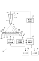
20…静電噴霧用ノズル、21…ノズル本体、22…分散液噴霧口、23…開口、24…芯構造、25…電極、26…ノズルホルダ、27…ノズル本体固定部、28…電圧供給端子、29…負圧導入口、30…基板ステージ、35…ステージ駆動装置、40…噴霧電圧印加装置、41…調整電圧印加装置、45…試料作製制御装置、46…表示装置、47…入力装置、
50…光分散用レーザ光源、55…凝集状態モニタ部、56…モニタ用光源、57…光検出装置、58…解析装置、
80…電圧印加用治具、81…基準電極(接地電極)、82…絶縁層、83…バイアス電極、85…開口部、86…電圧供給電極、87…電圧供給端子。
Claims (12)
- ナノ材料を観察基板上に固定化して観察試料を作製する作製装置であって、
ナノ材料が溶媒中に分散されたナノ材料分散液を内部に蓄えることが可能な筒状構造を有し、その先端部に前記ナノ材料分散液を静電噴霧するための分散液噴霧口が設けられたノズル本体を含む静電噴霧用ノズルと、
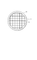
1または複数の開口を有するメッシュ状に形成された導電性のグリッド部、及び前記グリッド部の前記開口に設けられて観察対象の前記ナノ材料が固定化されるナノ材料支持膜を有する観察基板について、前記静電噴霧用ノズルの前記分散液噴霧口に対向するように前記観察基板を支持する基板支持手段と、
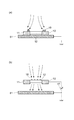
前記観察基板に対して前記静電噴霧用ノズルとは反対側に前記観察基板から離間するように配置され、基準電位と電気的に接続される基準電極と、
前記ナノ材料分散液と前記基準電極との間に、静電噴霧用の電圧を印加する噴霧電圧印加手段と、
前記観察基板の前記グリッド部と前記基準電極との間に、前記静電噴霧用の電圧と同一の極性であって、前記観察基板上での前記ナノ材料の固定化位置を調整するために用いられるバイアス電圧を印加する調整電圧印加手段と
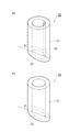
を備えることを特徴とする観察試料作製装置。 - 前記基準電極から離間して配置され、前記観察基板の前記グリッド部と電気的に接続されて、前記調整電圧印加手段からの前記バイアス電圧を前記グリッド部に印加するためのバイアス電極を備えることを特徴とする請求項1記載の観察試料作製装置。
- 前記基準電極と、前記バイアス電極と、前記基準電極及び前記バイアス電極の間に設けられた絶縁層とが一体化されて構成された電圧印加用治具を備えることを特徴とする請求項2記載の観察試料作製装置。
- 前記基準電極は、前記観察基板の前記ナノ材料支持膜に対向する位置を含むように配置されるとともに、
前記バイアス電極は、前記ナノ材料支持膜から前記基準電極が見通せるように設けられていることを特徴とする請求項2または3記載の観察試料作製装置。 - 前記バイアス電圧は、その絶対値が5V〜50Vの範囲内となるように設定された電圧であることを特徴とする請求項1〜4のいずれか一項記載の観察試料作製装置。
- 前記静電噴霧用ノズルの前記分散液噴霧口から前記観察基板へと前記ナノ材料分散液を静電噴霧する際に、噴霧された個々の液滴内に1個または0個のナノ材料が含まれる条件となるように、前記噴霧電圧印加手段によって印加される前記静電噴霧用の電圧を制御する電圧制御手段を備えることを特徴とする請求項1〜5のいずれか一項記載の観察試料作製装置。
- ナノ材料を観察基板上に固定化して観察試料を作製する作製方法であって、
ナノ材料が溶媒中に分散されたナノ材料分散液を内部に蓄えることが可能な筒状構造を有し、その先端部に前記ナノ材料分散液を静電噴霧するための分散液噴霧口が設けられたノズル本体を含む静電噴霧用ノズルを用い、前記ノズル本体の内部に前記ナノ材料分散液を導入する分散液導入ステップと、
1または複数の開口を有するメッシュ状に形成された導電性のグリッド部、及び前記グリッド部の前記開口に設けられて観察対象の前記ナノ材料が固定化されるナノ材料支持膜を有する観察基板について、前記静電噴霧用ノズルの前記分散液噴霧口に対向するように前記観察基板を設置する基板設置ステップと、
前記観察基板に対して前記静電噴霧用ノズルとは反対側に前記観察基板から離間するように配置され、基準電位と電気的に接続される基準電極に対し、前記ナノ材料分散液と前記基準電極との間に、静電噴霧用の電圧を印加する噴霧電圧印加ステップと、
前記観察基板の前記グリッド部と前記基準電極との間に、前記静電噴霧用の電圧と同一の極性であって、前記観察基板上での前記ナノ材料の固定化位置を調整するために用いられるバイアス電圧を印加する調整電圧印加ステップと、
前記静電噴霧用ノズルの前記分散液噴霧口から前記観察基板へと前記ナノ材料分散液を静電噴霧し、前記ナノ材料を前記観察基板の表面に静電付着させることで、前記観察基板上に前記ナノ材料を固定化して観察試料を作製する試料作製ステップと
を備えることを特徴とする観察試料作製方法。 - 前記調整電圧印加ステップにおいて、前記基準電極から離間して配置され、前記観察基板の前記グリッド部と電気的に接続されたバイアス電極を介して、前記バイアス電圧を前記グリッド部に印加することを特徴とする請求項7記載の観察試料作製方法。
- 前記調整電圧印加ステップにおいて、前記基準電極と、前記バイアス電極と、前記基準電極及び前記バイアス電極の間に設けられた絶縁層とが一体化されて構成された電圧印加用治具を用いることを特徴とする請求項8記載の観察試料作製方法。
- 前記基準電極は、前記観察基板の前記ナノ材料支持膜に対向する位置を含むように配置されるとともに、
前記バイアス電極は、前記ナノ材料支持膜から前記基準電極が見通せるように設けられていることを特徴とする請求項8または9記載の観察試料作製方法。 - 前記バイアス電圧は、その絶対値が5V〜50Vの範囲内となるように設定された電圧であることを特徴とする請求項7〜10のいずれか一項記載の観察試料作製方法。
- 前記試料作製ステップにおいて、噴霧された個々の液滴内に1個または0個のナノ材料が含まれる条件下で、前記静電噴霧用ノズルの前記分散液噴霧口から前記観察基板へと前記ナノ材料分散液を静電噴霧することを特徴とする請求項7〜11のいずれか一項記載の観察試料作製方法。
Priority Applications (2)
| Application Number | Priority Date | Filing Date | Title |
|---|---|---|---|
| JP2008026847A JP4974923B2 (ja) | 2008-02-06 | 2008-02-06 | ナノ材料の観察試料作製装置及び作製方法 |
| US12/365,256 US8276539B2 (en) | 2008-02-06 | 2009-02-04 | Nanomaterial observation sample preparation apparatus and preparation method |
Applications Claiming Priority (1)
| Application Number | Priority Date | Filing Date | Title |
|---|---|---|---|
| JP2008026847A JP4974923B2 (ja) | 2008-02-06 | 2008-02-06 | ナノ材料の観察試料作製装置及び作製方法 |
Publications (2)
| Publication Number | Publication Date |
|---|---|
| JP2009186332A JP2009186332A (ja) | 2009-08-20 |
| JP4974923B2 true JP4974923B2 (ja) | 2012-07-11 |
Family
ID=40930599
Family Applications (1)
| Application Number | Title | Priority Date | Filing Date |
|---|---|---|---|
| JP2008026847A Expired - Fee Related JP4974923B2 (ja) | 2008-02-06 | 2008-02-06 | ナノ材料の観察試料作製装置及び作製方法 |
Country Status (2)
| Country | Link |
|---|---|
| US (1) | US8276539B2 (ja) |
| JP (1) | JP4974923B2 (ja) |
Cited By (1)
| Publication number | Priority date | Publication date | Assignee | Title |
|---|---|---|---|---|
| CN111515069A (zh) * | 2020-04-26 | 2020-08-11 | 上海谷柏特汽车科技有限公司 | 一种汽车部件静电喷涂与机械臂联动装置 |
Families Citing this family (12)
| Publication number | Priority date | Publication date | Assignee | Title |
|---|---|---|---|---|
| US8058627B2 (en) * | 2008-08-13 | 2011-11-15 | Wisys Technology Foundation | Addressable transmission electron microscope grid |
| JP5919456B2 (ja) * | 2010-07-15 | 2016-05-18 | 合同会社アシスト技研 | 静電塗装装置 |
| KR101099766B1 (ko) | 2010-12-02 | 2011-12-28 | 양성식 | 나노 스프레이 코팅 장치 |
| JP6275001B2 (ja) * | 2014-08-14 | 2018-02-07 | 国立大学法人金沢大学 | エアロゾル捕集装置 |
| JP6672575B2 (ja) * | 2016-03-25 | 2020-03-25 | アネスト岩田株式会社 | 静電噴霧装置 |
| EP3502654A1 (en) * | 2017-12-22 | 2019-06-26 | Universiteit Maastricht | Method for applying liquids to a substrate |
| CN110632105B (zh) * | 2019-09-17 | 2021-10-29 | 东南大学 | 一种用于透射电镜表征的液体样品腔及其制备方法 |
| JP7401277B2 (ja) * | 2019-12-04 | 2023-12-19 | ファナック株式会社 | ロボットプログラミング装置 |
| IT202000004678A1 (it) * | 2020-03-05 | 2021-09-05 | Milano Politecnico | Sistema per la deposizione di microparticelle |
| JP7585113B2 (ja) | 2020-05-15 | 2024-11-18 | 株式会社堀場製作所 | 試料分散装置及び試料分散方法 |
| US12117379B2 (en) | 2020-05-15 | 2024-10-15 | Horiba, Ltd. | Sample dispersing device and sample dispersing method |
| CN114397278A (zh) * | 2021-12-24 | 2022-04-26 | 西湖大学 | 一种用于原位等离子共振的纳米颗粒基底及其制备方法和在特异性检测中的应用 |
Family Cites Families (9)
| Publication number | Priority date | Publication date | Assignee | Title |
|---|---|---|---|---|
| JPS62238439A (ja) * | 1986-04-09 | 1987-10-19 | Toyota Motor Corp | 電子顕微鏡の検鏡試料の採取方法およびその装置 |
| JPH05290779A (ja) * | 1992-04-09 | 1993-11-05 | Matsushita Electric Ind Co Ltd | 透過電子顕微鏡用試料の作製方法 |
| US5948483A (en) * | 1997-03-25 | 1999-09-07 | The Board Of Trustees Of The University Of Illinois | Method and apparatus for producing thin film and nanoparticle deposits |
| ATE464123T1 (de) * | 1997-06-20 | 2010-04-15 | Univ New York | Elektrosprühen von lösungen zur massenherstellung von chips und molekülbibliotheken |
| JP4425420B2 (ja) * | 2000-04-03 | 2010-03-03 | 独立行政法人理化学研究所 | マイクロアレイ作製装置 |
| CA2516422A1 (en) * | 2003-02-19 | 2004-09-02 | Akihiko Tanioka | Immobilizing method, immobilization apparatus, and microstructure manufacturing method |
| JP2005125181A (ja) * | 2003-10-22 | 2005-05-19 | Matsushita Electric Ind Co Ltd | 塗布方法および塗布装置 |
| KR100668343B1 (ko) * | 2005-08-12 | 2007-01-12 | 삼성전자주식회사 | 전기전하집중 현상을 이용하여 기판 상에 생체분자 액적을프린팅하는 장치 및 전기전하집중 현상을 이용하여인쇄용지 또는 인쇄기판 상에 잉크를 프린팅하는 장치 |
| JP5207334B2 (ja) * | 2006-02-28 | 2013-06-12 | 独立行政法人理化学研究所 | マイクロパターン形成装置、マイクロパターン構造体、および、その製造方法 |
-
2008
- 2008-02-06 JP JP2008026847A patent/JP4974923B2/ja not_active Expired - Fee Related
-
2009
- 2009-02-04 US US12/365,256 patent/US8276539B2/en not_active Expired - Fee Related
Cited By (1)
| Publication number | Priority date | Publication date | Assignee | Title |
|---|---|---|---|---|
| CN111515069A (zh) * | 2020-04-26 | 2020-08-11 | 上海谷柏特汽车科技有限公司 | 一种汽车部件静电喷涂与机械臂联动装置 |
Also Published As
| Publication number | Publication date |
|---|---|
| JP2009186332A (ja) | 2009-08-20 |
| US8276539B2 (en) | 2012-10-02 |
| US20090194418A1 (en) | 2009-08-06 |
Similar Documents
| Publication | Publication Date | Title |
|---|---|---|
| JP4974923B2 (ja) | ナノ材料の観察試料作製装置及び作製方法 | |
| JP5283918B2 (ja) | 静電噴霧用ノズルを用いたナノ材料固定化装置、固定化方法 | |
| JP5491189B2 (ja) | 固定化装置 | |
| KR20140040177A (ko) | 기판 상에 1d, 2d 또는 3d 구조물을 나노드리핑하는 방법 | |
| JP6264275B2 (ja) | マトリックス膜形成装置 | |
| JP5159348B2 (ja) | ナノ材料固定化方法及び固定化装置 | |
| US20180049406A1 (en) | Method for tagging insects and arthropods | |
| EP2532020A1 (en) | Multi-needle multi-parallel nanospray ionization source | |
| US20130228700A1 (en) | Method and apparatus for a porous electrospray emitter | |
| CN101321899A (zh) | 电流体力学印刷和制造 | |
| JP2013525785A (ja) | 表面増強発光のための自己配列型発光強化装置 | |
| CN101042977B (zh) | 碳纳米管场发射电子源及其制造方法以及一场发射阵列 | |
| KR101903712B1 (ko) | 패턴라인 형성장치 | |
| IL261919B2 (en) | A bottom-up method for creating wire structures on a substrate | |
| CN101051595B (zh) | 碳纳米管场发射电子源 | |
| Tepper et al. | A study of ionization and collection efficiencies in electrospray-based electrostatic precipitators | |
| KR20110070031A (ko) | 원자간력 현미경 탐침의 팁용 탄소나노튜브 부착방법 및 그 방법에 의해 팁에 탄소나노튜브가 부착된 원자간력 현미경용 탐침 | |
| US20240431215A1 (en) | Fabrication of a scalable quantum sensing device through precisely programmable patterning spin defects on universal substrates | |
| Wang et al. | Development of a thermoelectric nanowire characterization platform (TNCP) for structural and thermoelectric investigation of single nanowires | |
| CN101051596B (zh) | 碳纳米管场发射电子源及其制造方法 | |
| JP2006085935A (ja) | 電界放出デバイスの製造方法および電界放出デバイス | |
| KR20060013379A (ko) | 전계 방출 전극의 제조방법 | |
| JP7780551B2 (ja) | エレクトロスプレー発生装置用エミッタを製造するための方法 | |
| Soh | Functionalising AFM tips for pick and place manipulation of micro and nanoparticles | |
| JP7085326B2 (ja) | 液中粒子の捕集装置及び捕集方法 |
Legal Events
| Date | Code | Title | Description |
|---|---|---|---|
| A621 | Written request for application examination |
Free format text: JAPANESE INTERMEDIATE CODE: A621 Effective date: 20100922 |
|
| A977 | Report on retrieval |
Free format text: JAPANESE INTERMEDIATE CODE: A971007 Effective date: 20120228 |
|
| TRDD | Decision of grant or rejection written | ||
| A01 | Written decision to grant a patent or to grant a registration (utility model) |
Free format text: JAPANESE INTERMEDIATE CODE: A01 Effective date: 20120403 |
|
| A01 | Written decision to grant a patent or to grant a registration (utility model) |
Free format text: JAPANESE INTERMEDIATE CODE: A01 |
|
| A61 | First payment of annual fees (during grant procedure) |
Free format text: JAPANESE INTERMEDIATE CODE: A61 Effective date: 20120410 |
|
| R150 | Certificate of patent or registration of utility model |
Ref document number: 4974923 Country of ref document: JP Free format text: JAPANESE INTERMEDIATE CODE: R150 Free format text: JAPANESE INTERMEDIATE CODE: R150 |
|
| FPAY | Renewal fee payment (event date is renewal date of database) |
Free format text: PAYMENT UNTIL: 20150420 Year of fee payment: 3 |
|
| LAPS | Cancellation because of no payment of annual fees |