JP4981491B2 - インクジェットヘッド製造方法及び貫通電極の製造方法 - Google Patents
インクジェットヘッド製造方法及び貫通電極の製造方法 Download PDFInfo
- Publication number
- JP4981491B2 JP4981491B2 JP2007066585A JP2007066585A JP4981491B2 JP 4981491 B2 JP4981491 B2 JP 4981491B2 JP 2007066585 A JP2007066585 A JP 2007066585A JP 2007066585 A JP2007066585 A JP 2007066585A JP 4981491 B2 JP4981491 B2 JP 4981491B2
- Authority
- JP
- Japan
- Prior art keywords
- substrate
- manufacturing
- ink
- etching
- hole
- Prior art date
- Legal status (The legal status is an assumption and is not a legal conclusion. Google has not performed a legal analysis and makes no representation as to the accuracy of the status listed.)
- Expired - Fee Related
Links
Images




Classifications
-
- B—PERFORMING OPERATIONS; TRANSPORTING
- B41—PRINTING; LINING MACHINES; TYPEWRITERS; STAMPS
- B41J—TYPEWRITERS; SELECTIVE PRINTING MECHANISMS, i.e. MECHANISMS PRINTING OTHERWISE THAN FROM A FORME; CORRECTION OF TYPOGRAPHICAL ERRORS
- B41J2/00—Typewriters or selective printing mechanisms characterised by the printing or marking process for which they are designed
- B41J2/005—Typewriters or selective printing mechanisms characterised by the printing or marking process for which they are designed characterised by bringing liquid or particles selectively into contact with a printing material
- B41J2/01—Ink jet
- B41J2/135—Nozzles
- B41J2/16—Production of nozzles
- B41J2/1601—Production of bubble jet print heads
- B41J2/1603—Production of bubble jet print heads of the front shooter type
-
- B—PERFORMING OPERATIONS; TRANSPORTING
- B41—PRINTING; LINING MACHINES; TYPEWRITERS; STAMPS
- B41J—TYPEWRITERS; SELECTIVE PRINTING MECHANISMS, i.e. MECHANISMS PRINTING OTHERWISE THAN FROM A FORME; CORRECTION OF TYPOGRAPHICAL ERRORS
- B41J2/00—Typewriters or selective printing mechanisms characterised by the printing or marking process for which they are designed
- B41J2/005—Typewriters or selective printing mechanisms characterised by the printing or marking process for which they are designed characterised by bringing liquid or particles selectively into contact with a printing material
- B41J2/01—Ink jet
- B41J2/135—Nozzles
- B41J2/16—Production of nozzles
- B41J2/1621—Manufacturing processes
- B41J2/1626—Manufacturing processes etching
- B41J2/1628—Manufacturing processes etching dry etching
-
- B—PERFORMING OPERATIONS; TRANSPORTING
- B41—PRINTING; LINING MACHINES; TYPEWRITERS; STAMPS
- B41J—TYPEWRITERS; SELECTIVE PRINTING MECHANISMS, i.e. MECHANISMS PRINTING OTHERWISE THAN FROM A FORME; CORRECTION OF TYPOGRAPHICAL ERRORS
- B41J2/00—Typewriters or selective printing mechanisms characterised by the printing or marking process for which they are designed
- B41J2/005—Typewriters or selective printing mechanisms characterised by the printing or marking process for which they are designed characterised by bringing liquid or particles selectively into contact with a printing material
- B41J2/01—Ink jet
- B41J2/135—Nozzles
- B41J2/16—Production of nozzles
- B41J2/1621—Manufacturing processes
- B41J2/1631—Manufacturing processes photolithography
-
- B—PERFORMING OPERATIONS; TRANSPORTING
- B41—PRINTING; LINING MACHINES; TYPEWRITERS; STAMPS
- B41J—TYPEWRITERS; SELECTIVE PRINTING MECHANISMS, i.e. MECHANISMS PRINTING OTHERWISE THAN FROM A FORME; CORRECTION OF TYPOGRAPHICAL ERRORS
- B41J2/00—Typewriters or selective printing mechanisms characterised by the printing or marking process for which they are designed
- B41J2/005—Typewriters or selective printing mechanisms characterised by the printing or marking process for which they are designed characterised by bringing liquid or particles selectively into contact with a printing material
- B41J2/01—Ink jet
- B41J2/135—Nozzles
- B41J2/16—Production of nozzles
- B41J2/1621—Manufacturing processes
- B41J2/1632—Manufacturing processes machining
-
- B—PERFORMING OPERATIONS; TRANSPORTING
- B41—PRINTING; LINING MACHINES; TYPEWRITERS; STAMPS
- B41J—TYPEWRITERS; SELECTIVE PRINTING MECHANISMS, i.e. MECHANISMS PRINTING OTHERWISE THAN FROM A FORME; CORRECTION OF TYPOGRAPHICAL ERRORS
- B41J2/00—Typewriters or selective printing mechanisms characterised by the printing or marking process for which they are designed
- B41J2/005—Typewriters or selective printing mechanisms characterised by the printing or marking process for which they are designed characterised by bringing liquid or particles selectively into contact with a printing material
- B41J2/01—Ink jet
- B41J2/135—Nozzles
- B41J2/16—Production of nozzles
- B41J2/1621—Manufacturing processes
- B41J2/1637—Manufacturing processes molding
- B41J2/1639—Manufacturing processes molding sacrificial molding
-
- B—PERFORMING OPERATIONS; TRANSPORTING
- B41—PRINTING; LINING MACHINES; TYPEWRITERS; STAMPS
- B41J—TYPEWRITERS; SELECTIVE PRINTING MECHANISMS, i.e. MECHANISMS PRINTING OTHERWISE THAN FROM A FORME; CORRECTION OF TYPOGRAPHICAL ERRORS
- B41J2/00—Typewriters or selective printing mechanisms characterised by the printing or marking process for which they are designed
- B41J2/005—Typewriters or selective printing mechanisms characterised by the printing or marking process for which they are designed characterised by bringing liquid or particles selectively into contact with a printing material
- B41J2/01—Ink jet
- B41J2/135—Nozzles
- B41J2/16—Production of nozzles
- B41J2/1621—Manufacturing processes
- B41J2/164—Manufacturing processes thin film formation
- B41J2/1642—Manufacturing processes thin film formation thin film formation by CVD [chemical vapor deposition]
-
- B—PERFORMING OPERATIONS; TRANSPORTING
- B41—PRINTING; LINING MACHINES; TYPEWRITERS; STAMPS
- B41J—TYPEWRITERS; SELECTIVE PRINTING MECHANISMS, i.e. MECHANISMS PRINTING OTHERWISE THAN FROM A FORME; CORRECTION OF TYPOGRAPHICAL ERRORS
- B41J2/00—Typewriters or selective printing mechanisms characterised by the printing or marking process for which they are designed
- B41J2/005—Typewriters or selective printing mechanisms characterised by the printing or marking process for which they are designed characterised by bringing liquid or particles selectively into contact with a printing material
- B41J2/01—Ink jet
- B41J2/135—Nozzles
- B41J2/16—Production of nozzles
- B41J2/1621—Manufacturing processes
- B41J2/164—Manufacturing processes thin film formation
- B41J2/1643—Manufacturing processes thin film formation thin film formation by plating
-
- B—PERFORMING OPERATIONS; TRANSPORTING
- B41—PRINTING; LINING MACHINES; TYPEWRITERS; STAMPS
- B41J—TYPEWRITERS; SELECTIVE PRINTING MECHANISMS, i.e. MECHANISMS PRINTING OTHERWISE THAN FROM A FORME; CORRECTION OF TYPOGRAPHICAL ERRORS
- B41J2/00—Typewriters or selective printing mechanisms characterised by the printing or marking process for which they are designed
- B41J2/005—Typewriters or selective printing mechanisms characterised by the printing or marking process for which they are designed characterised by bringing liquid or particles selectively into contact with a printing material
- B41J2/01—Ink jet
- B41J2/135—Nozzles
- B41J2/16—Production of nozzles
- B41J2/1621—Manufacturing processes
- B41J2/164—Manufacturing processes thin film formation
- B41J2/1645—Manufacturing processes thin film formation thin film formation by spincoating
-
- B—PERFORMING OPERATIONS; TRANSPORTING
- B41—PRINTING; LINING MACHINES; TYPEWRITERS; STAMPS
- B41J—TYPEWRITERS; SELECTIVE PRINTING MECHANISMS, i.e. MECHANISMS PRINTING OTHERWISE THAN FROM A FORME; CORRECTION OF TYPOGRAPHICAL ERRORS
- B41J2/00—Typewriters or selective printing mechanisms characterised by the printing or marking process for which they are designed
- B41J2/005—Typewriters or selective printing mechanisms characterised by the printing or marking process for which they are designed characterised by bringing liquid or particles selectively into contact with a printing material
- B41J2/01—Ink jet
- B41J2/135—Nozzles
- B41J2/16—Production of nozzles
- B41J2/1621—Manufacturing processes
- B41J2/164—Manufacturing processes thin film formation
- B41J2/1646—Manufacturing processes thin film formation thin film formation by sputtering
Landscapes
- Engineering & Computer Science (AREA)
- Manufacturing & Machinery (AREA)
- Particle Formation And Scattering Control In Inkjet Printers (AREA)
Description
本実施例1では、前述の手順でインクジェットヘッドを作製した。
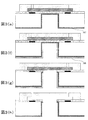
はじめに、図3(a)エネルギー発生素子102及び素子駆動用回路(図示せず)が複数個配置された基板101上に、後に溶解可能な樹脂層としてインク流路型材103となるパターンを形成する。ここでは、東京応化工業社製ODUR−1010をUSHIO社製UX−3000を用いてDEEPUV光で約20000mJ/cm2の照射を行いパターニングした。次いで、インク流路型材となるパターン上に下記表1の組成からなるネガ型感光性樹脂をスピンコートした。次いで、この樹脂層をキヤノン社製ミラープロジェクションアライナー(MPA−600Super)のUV光にて露光、現像し、インク吐出口104を形成した(以上図3(b))。

本実施例2では、基板を貫通する貫通電極を作製した。
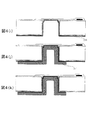
はじめに、図4(a)に示したようなアルミの配線パターン202が形成された基板201上に、透明電極203としてITO(酸化インジウム薄膜)を形成した(図4(b))。これは、貫通部に光透過性を持たせるためのものであるので、最低限、貫通部分とその近傍のみにパターンを形成すればよい。
102 吐出圧力発生素子
103 インク流路型材
104 インク吐出口
105 インク供給口パターン
106 インク供給口
107 耐インク保護膜
108 ポジ型レジスト
109 エッチングストップ層
201 基板
202 アルミ配線パターン
203 透明電極
205 貫通電極パターン
206 貫通口
207 絶縁膜
208 ポジ型レジスト
209 エッチングストップ層
210 シード層
211 導電層
301 フォトマスク
302 遮光膜のパターン
Claims (8)
- インクを吐出する吐出口と、前記吐出口へインクを供給するための供給口が形成された基板と、を有するインクジェットヘッドの製造方法において、
インク供給口を形成するために、前記基板の一方の面側から前記基板をエッチングすることにより貫通口を形成する工程と、
前記貫通口の内壁および貫通部分を被覆するように保護膜を形成する工程と、
前記保護膜にポジ型レジストを積層し、前記基板の前記一方の面と対向する面側から前記基板を介さずに光をプロジェクション方式で照射して、前記ポジ型レジストをパターニングする工程と、
パターニングされた前記ポジ型レジストをマスクとして前記貫通口の貫通部分の前記保護膜をエッチングする工程と、
を有することを特徴とするインクジェットヘッドの製造方法。 - 光を照射する際にフォトマスクを用いることを特徴とする請求項1に記載のインクジェットヘッドの製造方法。
- 光を照射する際にマスクとなる遮光膜をあらかじめ前記基板の一方の面に形成することを特徴とする請求項1に記載のインクジェットヘッドの製造方法。
- 基板を貫通する貫通電極を形成するために基板の一方の面側から基板をエッチングして貫通口を形成する工程と、
前記貫通口の内壁および貫通部に絶縁膜を形成する工程と、
前記絶縁膜にポジ型レジストを積層し、前記基板の一方の面と対向する面側から前記基板を介さずに光をプロジェクション方式で照射して、前記ポジ型レジストをパターニングする工程と、
パターニングされた前記ポジ型レジストをマスクとして前記貫通口の貫通部分の前記絶縁膜をエッチングする工程と、
を有することを特徴とする貫通電極の製造方法。
- 光を照射する際にフォトマスクを用いることを特徴とする請求項4に記載の貫通電極の製造方法。
- 光を照射する際に、マスクとなる遮光膜をあらかじめ前記基板の前記一方の面側に形成しておくことを特徴とする請求項4に記載の貫通電極の製造方法。
- 前記基板の一方の面側に形成される電気配線パターンの少なくとも一部に導電性透明膜を用いていることを特徴とする請求項4に記載の貫通電極の製造方法。
- 前記導電性透明膜がITO(酸化インジウム薄膜)であることを特徴とする請求項7に記載の貫通電極の製造方法。
Priority Applications (2)
| Application Number | Priority Date | Filing Date | Title |
|---|---|---|---|
| JP2007066585A JP4981491B2 (ja) | 2007-03-15 | 2007-03-15 | インクジェットヘッド製造方法及び貫通電極の製造方法 |
| US12/042,695 US7985531B2 (en) | 2007-03-15 | 2008-03-05 | Method of producing an ink jet head and method of producing an electronic device |
Applications Claiming Priority (1)
| Application Number | Priority Date | Filing Date | Title |
|---|---|---|---|
| JP2007066585A JP4981491B2 (ja) | 2007-03-15 | 2007-03-15 | インクジェットヘッド製造方法及び貫通電極の製造方法 |
Publications (2)
| Publication Number | Publication Date |
|---|---|
| JP2008221757A JP2008221757A (ja) | 2008-09-25 |
| JP4981491B2 true JP4981491B2 (ja) | 2012-07-18 |
Family
ID=39763057
Family Applications (1)
| Application Number | Title | Priority Date | Filing Date |
|---|---|---|---|
| JP2007066585A Expired - Fee Related JP4981491B2 (ja) | 2007-03-15 | 2007-03-15 | インクジェットヘッド製造方法及び貫通電極の製造方法 |
Country Status (2)
| Country | Link |
|---|---|
| US (1) | US7985531B2 (ja) |
| JP (1) | JP4981491B2 (ja) |
Families Citing this family (15)
| Publication number | Priority date | Publication date | Assignee | Title |
|---|---|---|---|---|
| US8376525B2 (en) * | 2006-09-08 | 2013-02-19 | Canon Kabushiki Kaisha | Liquid discharge head and method of manufacturing the same |
| JP2009119650A (ja) * | 2007-11-13 | 2009-06-04 | Canon Inc | インクジェットヘッドの製造方法 |
| US20090136875A1 (en) * | 2007-11-15 | 2009-05-28 | Canon Kabushiki Kaisha | Manufacturing method of liquid ejection head |
| US20090162797A1 (en) * | 2007-12-19 | 2009-06-25 | Canon Kabushiki Kaisha | Method of manufacturing liquid ejection head |
| JP2009220286A (ja) * | 2008-03-13 | 2009-10-01 | Canon Inc | 液体吐出記録ヘッド及その製造方法 |
| JP4942218B2 (ja) * | 2008-12-16 | 2012-05-30 | キヤノン株式会社 | 液体吐出ヘッドの製造方法 |
| JP5574802B2 (ja) * | 2009-06-03 | 2014-08-20 | キヤノン株式会社 | 構造体の製造方法 |
| JP5967876B2 (ja) | 2010-09-21 | 2016-08-10 | キヤノン株式会社 | 液体吐出ヘッド及びその製造方法 |
| JP2013028110A (ja) * | 2011-07-29 | 2013-02-07 | Canon Inc | 液体吐出ヘッド用基板の製造方法 |
| JP5769560B2 (ja) | 2011-09-09 | 2015-08-26 | キヤノン株式会社 | 液体吐出ヘッド用基体及びその製造方法 |
| US8465823B1 (en) * | 2011-12-22 | 2013-06-18 | Oracle International Corporation | Optical media having transparent back side coating |
| JP2013230589A (ja) * | 2012-04-27 | 2013-11-14 | Canon Inc | 液体吐出ヘッドの製造方法 |
| US10022979B2 (en) | 2016-01-08 | 2018-07-17 | Canon Kabushiki Kaisha | Liquid ejection head, liquid ejection apparatus, and manufacturing method |
| JP7020407B2 (ja) * | 2016-06-15 | 2022-02-16 | ソニーグループ株式会社 | 半導体装置、及び、半導体装置の製造方法 |
| JP7009225B2 (ja) | 2018-01-16 | 2022-01-25 | キヤノン株式会社 | 構造体の製造方法、液体吐出ヘッドの製造方法、保護部材、保護基板及び保護基板の製造方法 |
Family Cites Families (17)
| Publication number | Priority date | Publication date | Assignee | Title |
|---|---|---|---|---|
| JP3143307B2 (ja) | 1993-02-03 | 2001-03-07 | キヤノン株式会社 | インクジェット記録ヘッドの製造方法 |
| US6461798B1 (en) | 1995-03-31 | 2002-10-08 | Canon Kabushiki Kaisha | Process for the production of an ink jet head |
| JPH0911478A (ja) | 1995-06-27 | 1997-01-14 | Canon Inc | インクジェット記録ヘッドの製造方法 |
| JP3343875B2 (ja) * | 1995-06-30 | 2002-11-11 | キヤノン株式会社 | インクジェットヘッドの製造方法 |
| JPH10128985A (ja) * | 1996-11-05 | 1998-05-19 | Canon Inc | インクジェット記録ヘッドの製造方法 |
| JPH10283927A (ja) * | 1997-04-09 | 1998-10-23 | Dainippon Printing Co Ltd | Ac型プラズマディスプレイパネル及びその蛍光面形成方法 |
| JP2000255063A (ja) * | 1999-03-05 | 2000-09-19 | Casio Comput Co Ltd | インクジェットプリンタ |
| JP4522086B2 (ja) * | 2003-12-15 | 2010-08-11 | キヤノン株式会社 | 梁、梁の製造方法、梁を備えたインクジェット記録ヘッド、および該インクジェット記録ヘッドの製造方法 |
| JP4537246B2 (ja) | 2004-05-06 | 2010-09-01 | キヤノン株式会社 | インクジェット記録ヘッド用基体の製造方法及び該方法により製造された前記基体を用いた記録ヘッドの製造方法 |
| US7629111B2 (en) | 2004-06-28 | 2009-12-08 | Canon Kabushiki Kaisha | Liquid discharge head manufacturing method, and liquid discharge head obtained using this method |
| CN1968815B (zh) | 2004-06-28 | 2013-05-01 | 佳能株式会社 | 排液头制造方法,和使用该方法得到的排液头 |
| JP4564342B2 (ja) * | 2004-11-24 | 2010-10-20 | 大日本印刷株式会社 | 多層配線基板およびその製造方法 |
| JP4459037B2 (ja) | 2004-12-01 | 2010-04-28 | キヤノン株式会社 | 液体吐出ヘッド |
| JP4614383B2 (ja) | 2004-12-09 | 2011-01-19 | キヤノン株式会社 | インクジェット記録ヘッドの製造方法、及びインクジェット記録ヘッド |
| JP4766658B2 (ja) * | 2005-05-10 | 2011-09-07 | キヤノン株式会社 | 液体吐出ヘッドおよびその製造方法 |
| US8037603B2 (en) | 2006-04-27 | 2011-10-18 | Canon Kabushiki Kaisha | Ink jet head and producing method therefor |
| US8241510B2 (en) * | 2007-01-22 | 2012-08-14 | Canon Kabushiki Kaisha | Inkjet recording head, method for producing same, and semiconductor device |
-
2007
- 2007-03-15 JP JP2007066585A patent/JP4981491B2/ja not_active Expired - Fee Related
-
2008
- 2008-03-05 US US12/042,695 patent/US7985531B2/en not_active Expired - Fee Related
Also Published As
| Publication number | Publication date |
|---|---|
| JP2008221757A (ja) | 2008-09-25 |
| US7985531B2 (en) | 2011-07-26 |
| US20080227035A1 (en) | 2008-09-18 |
Similar Documents
| Publication | Publication Date | Title |
|---|---|---|
| JP4981491B2 (ja) | インクジェットヘッド製造方法及び貫通電極の製造方法 | |
| CN102802958B (zh) | 具有耐溶剂性的热喷墨印刷头 | |
| JP5495623B2 (ja) | 基板の加工方法、液体吐出ヘッド用基板の製造方法および液体吐出ヘッドの製造方法 | |
| JP5693068B2 (ja) | 液体吐出ヘッド及びその製造方法 | |
| JP2009096036A (ja) | 記録ヘッド基板及びその製造方法 | |
| JP6029316B2 (ja) | 液体吐出ヘッドの製造方法 | |
| JP2008179045A (ja) | インクジェット記録ヘッド及びその製造方法、半導体デバイス及びその製造方法 | |
| US20130161286A1 (en) | Processing method for an ink jet head substrate | |
| JP5980020B2 (ja) | 液体吐出ヘッド用基板の製造方法 | |
| JP2004042396A (ja) | 微細構造体の製造方法、液体吐出ヘッドの製造方法および液体吐出ヘッド | |
| JP6157180B2 (ja) | インクジェット記録ヘッドおよびその製造方法 | |
| US10894410B2 (en) | Method of manufacturing liquid ejection head and method of forming resist | |
| JP6099891B2 (ja) | ドライエッチング方法 | |
| US8398212B2 (en) | Ink jet head and method of manufacturing the same | |
| US8999182B2 (en) | Method for manufacturing liquid discharge head | |
| JP2012121168A (ja) | 液体吐出ヘッド及びその製造方法 | |
| JP2014198386A (ja) | インク吐出ヘッドの製造方法 | |
| JP2009255415A (ja) | インクジェット記録ヘッドの製造方法 | |
| JP6961453B2 (ja) | 貫通基板の加工方法および液体吐出ヘッドの製造方法 | |
| JP6000831B2 (ja) | 液体吐出ヘッドの製造方法 | |
| JP6032955B2 (ja) | 液体吐出ヘッドの製造方法 | |
| JP2005161595A (ja) | インクジェット記録ヘッドおよびその製造方法 | |
| JPH08244236A (ja) | 液体噴射記録ヘッドの製造方法 | |
| JPH0985957A (ja) | 液体噴射記録ヘッドの製造方法 | |
| JP2015155176A (ja) | 液体吐出ヘッドの製造方法及び液体吐出ヘッド |
Legal Events
| Date | Code | Title | Description |
|---|---|---|---|
| A621 | Written request for application examination |
Free format text: JAPANESE INTERMEDIATE CODE: A621 Effective date: 20100224 |
|
| A131 | Notification of reasons for refusal |
Free format text: JAPANESE INTERMEDIATE CODE: A131 Effective date: 20110928 |
|
| A977 | Report on retrieval |
Free format text: JAPANESE INTERMEDIATE CODE: A971007 Effective date: 20110928 |
|
| A521 | Written amendment |
Free format text: JAPANESE INTERMEDIATE CODE: A523 Effective date: 20111128 |
|
| A131 | Notification of reasons for refusal |
Free format text: JAPANESE INTERMEDIATE CODE: A131 Effective date: 20120214 |
|
| A521 | Written amendment |
Free format text: JAPANESE INTERMEDIATE CODE: A523 Effective date: 20120313 |
|
| TRDD | Decision of grant or rejection written | ||
| A01 | Written decision to grant a patent or to grant a registration (utility model) |
Free format text: JAPANESE INTERMEDIATE CODE: A01 Effective date: 20120417 |
|
| A01 | Written decision to grant a patent or to grant a registration (utility model) |
Free format text: JAPANESE INTERMEDIATE CODE: A01 |
|
| A61 | First payment of annual fees (during grant procedure) |
Free format text: JAPANESE INTERMEDIATE CODE: A61 Effective date: 20120420 |
|
| FPAY | Renewal fee payment (event date is renewal date of database) |
Free format text: PAYMENT UNTIL: 20150427 Year of fee payment: 3 |
|
| R151 | Written notification of patent or utility model registration |
Ref document number: 4981491 Country of ref document: JP Free format text: JAPANESE INTERMEDIATE CODE: R151 |
|
| LAPS | Cancellation because of no payment of annual fees |