JP4982015B2 - Reflector for UV lamp system - Google Patents
Reflector for UV lamp system Download PDFInfo
- Publication number
- JP4982015B2 JP4982015B2 JP2001274905A JP2001274905A JP4982015B2 JP 4982015 B2 JP4982015 B2 JP 4982015B2 JP 2001274905 A JP2001274905 A JP 2001274905A JP 2001274905 A JP2001274905 A JP 2001274905A JP 4982015 B2 JP4982015 B2 JP 4982015B2
- Authority
- JP
- Japan
- Prior art keywords
- reflector
- bulb
- radiation
- electromagnetic radiation
- equal
- Prior art date
- Legal status (The legal status is an assumption and is not a legal conclusion. Google has not performed a legal analysis and makes no representation as to the accuracy of the status listed.)
- Expired - Fee Related
Links
Images
Classifications
-
- G—PHYSICS
- G02—OPTICS
- G02B—OPTICAL ELEMENTS, SYSTEMS OR APPARATUS
- G02B5/00—Optical elements other than lenses
- G02B5/08—Mirrors
- G02B5/10—Mirrors with curved faces
-
- F—MECHANICAL ENGINEERING; LIGHTING; HEATING; WEAPONS; BLASTING
- F21—LIGHTING
- F21V—FUNCTIONAL FEATURES OR DETAILS OF LIGHTING DEVICES OR SYSTEMS THEREOF; STRUCTURAL COMBINATIONS OF LIGHTING DEVICES WITH OTHER ARTICLES, NOT OTHERWISE PROVIDED FOR
- F21V7/00—Reflectors for light sources
- F21V7/04—Optical design
-
- F—MECHANICAL ENGINEERING; LIGHTING; HEATING; WEAPONS; BLASTING
- F26—DRYING
- F26B—DRYING SOLID MATERIALS OR OBJECTS BY REMOVING LIQUID THEREFROM
- F26B3/00—Drying solid materials or objects by processes involving the application of heat
- F26B3/28—Drying solid materials or objects by processes involving the application of heat by radiation, e.g. from the sun
-
- H—ELECTRICITY
- H01—ELECTRIC ELEMENTS
- H01J—ELECTRIC DISCHARGE TUBES OR DISCHARGE LAMPS
- H01J65/00—Lamps without any electrode inside the vessel; Lamps with at least one main electrode outside the vessel
- H01J65/04—Lamps in which a gas filling is excited to luminesce by an external electromagnetic field or by external corpuscular radiation, e.g. for indicating plasma display panels
- H01J65/042—Lamps in which a gas filling is excited to luminesce by an external electromagnetic field or by external corpuscular radiation, e.g. for indicating plasma display panels by an external electromagnetic field
- H01J65/044—Lamps in which a gas filling is excited to luminesce by an external electromagnetic field or by external corpuscular radiation, e.g. for indicating plasma display panels by an external electromagnetic field the field being produced by a separate microwave unit
Landscapes
- Engineering & Computer Science (AREA)
- Physics & Mathematics (AREA)
- General Engineering & Computer Science (AREA)
- General Physics & Mathematics (AREA)
- Mechanical Engineering (AREA)
- Microbiology (AREA)
- Life Sciences & Earth Sciences (AREA)
- Optics & Photonics (AREA)
- Discharge Lamps And Accessories Thereof (AREA)
- Optical Elements Other Than Lenses (AREA)
- Physical Or Chemical Processes And Apparatus (AREA)
- Optical Filters (AREA)
- Non-Portable Lighting Devices Or Systems Thereof (AREA)
Description
【0001】
【発明の属する技術分野】
本発明は概して紫外線ランプシステムに関するものであり、特に紫外線ランプシステムにおいて用いられる、システム内に配設されたプラズマバルブの発生する紫外線放射を反射する反射器(反射器)に関するものである。
【0002】
【従来の技術】
紫外線ランプシステムは、該システム内のマイクロ波キャビティ即ちマイクロ波チャンバ内に設置された紫外線プラズマバルブのごとき無電極ランプにマイクロ波エネルギーを結合するようになされている。紫外線熱硬化においては、ランプシステムに1以上のマグネトロンを設け、マイクロ波放射をマイクロ波チャンバ内のプラズマバルブに結合している。マグネトロンはマイクロ波チャンバに対して、チャンバの上端に連結された出力ポートを有するウェーブガイドを介して結合されている。プラズマバルブはマイクロ波エネルギーにより十分に励起されているとき、マイクロ波チャンバの下端から、照射対象基板に向けて強い紫外および赤外成分を有する放射スペクトルを放つ。一般的には紫外線ランプシステムはまた、チャンバ下端に設けられた、紫外線は透過するがマグネトロンにより発生されたマイクロ波は透過しない金属網を有している。なおここで「上端」および「下端」とは図面に示されたチャンバの向きに関連してマイクロ波チャンバの説明を簡単にするために用いているものであることを理解されたい。当然ながら、紫外線ランプ加熱硬化の特定の適用例に応じて、マイクロ波チャンバの構造と機能を全く改変することなくマイクロ波チャンバの向きを変えることができる。
【0003】
プラズマバルブ(plasma bulb即ちプラズマ管あるいはプラズマ電球)は、特性スペクトルを有する近似的線光源を提供し、その長手方向に沿って外部に等方的に放射を射出する。しかし放出された放射の大部分は1回以上の反射を経て基板に到達する。例えば接着剤、シーラント、インク、塗膜材等の硬化または加熱に用いられる紫外線ランプシステムは、プラズマバルブが配置されるマイクロ波チャンバ内に取り付けられるかまたは該チャンバの一部をなす反射器を含む。反射器は反射された放射を所定パターンに従って基板に振り向けるよう機能する光学要素である。
【0004】
大部分の紫外線ランプシステムにおいては、冷光照明(cold-light illumination)が望まれる。冷光照明ではプラズマバルブの放つ放射の赤外成分をシステム内の吸収フィルタ又は反射フィルタにより除去しておく。赤外線放射は基板と相互作用し照射面を加熱する。従ってこのようなシステムの好適な反射器は放射を波長の関数として選択的に反射しかつ透過する。特に反射器を、紫外線を優先選択的に基板に導く波長選択的コーティングを有する被膜光学素子とすることができる。波長選択的コーティングは一般的には誘電体材料の多層薄膜であり、これは当業者にはよく知られた物理蒸着または化学蒸着などの真空蒸着技術を用いて塗膜される。赤外領域の波長を有する放射は反射器によって透過され、周囲構造に吸収されて熱的に放散される。従って余計な赤外放射は反射器によって実質的に反射されることはなく、基板を照明することもない。
【0005】
【発明が解決しようとする課題】
反射器の幾何学的形状は基板を照明する放射のパターンを決定する。反射器は通例、円錐を平面で切って得られる放物線、楕円、双曲線、円などの円錐曲線の一部の形状になされる。一般的には楕円形の反射器が用いられ、該反射器の焦点あるいはその近傍に置かれた基板に紫外線放射のフォーカスされた即ち収束されたビームを与える。楕円反射器の特性は、楕円の一つの焦点に位置する光源から放射された光線は反射器でいちど反射された後他方の焦点を通過する、というものである。こうして一方の焦点に沿って軸方向に置かれたプラズマバルブを有する楕円反射器は、第2の焦点に置かれた基板に対してフォーカスされた線状の放射を与えることになる。
【0006】
他方で、紫外線ランプシステムのいくつかの適用例では、基板の比較的広い面積にわたって一様な照射または放射密度が要求される。このような適用例に対しては、双曲線の焦点に置かれた放射源を有する双曲線反射器が理想的であろう。双曲線反射器のこのような線光源から発せられた間接放射は無限遠の焦点面に向かう共心の平行光線束として反射される。しかしながら、双曲線反射器は双曲線面に割り当てられる数学的記述に従って相対的に広いので、大抵の場合、双曲線反射器は大部分のマイクロ波チャンバの利用可能スペースに納めることが物理的にできない。
【0007】
過去において、反射器−プラズマバルブ−基板の光学的配置を調整することにより一様な放射を与えるように紫外線ランプシステムの設計が試みられてきた。より小型の反射器を提供するために提案された一つの解決策は、楕円反射器の焦点からプラズマバルブを離すように位置替えすることであった。この構成によって反射される紫外線放射は少なくとも部分的にデフォーカスされはしたが、照射は基板面にわたって十分に均一ではなかった。更に入射マイクロ波エネルギーとプラズマバルブ内のガスの結合が変化し、プラズマバルブの長さ方向に沿って照射が不均一になる。提案された別の解決策は、楕円反射器の位置を変えて基板が焦点面あるいはその近傍に位置しないようにするというものであった。しかし反射器を位置替えすることによりプラズマバルブに与えうる冷却が減少し、それに伴ってプラズマバルブの使用寿命が短くなる。
【0008】
以上の次第で、広い面積にわたって均一な紫外線放射を効率的に提供し、かつマイクロ波チャンバの最適な寸法と干渉することがなく、あるいはプラズマバルブの動作特性に悪影響を及ぼさないようになされた反射器が求められている。
【0009】
【課題を解決するための手段】
本発明は現在知られているマイクロ波励起式紫外線ランプシステムの上記およびその他の欠点を解消するものである。後に本発明を或る実施の形態に関連して説明するが、本発明はそれら実施形態に限定されるものではない。むしろ本発明は本発明の概念と範囲の内に含まれるであろうすべての代替的構成、変形例、均等物を含むものである。
【0010】
本発明による反射器は、紫外線ランプシステムのプラズマバルブから離間して設けられるようになされた長手に延びる1つ以上の反射パネルを有する。この反射器はプラズマバルブの発する電磁放射、特に紫外線放射を反射し、隣接する基板の表面に上にほぼ均一な照射をもたらすことができる。各反射パネルの主要部の湾曲はデカルト座標において、式(x/a)(2+n)+(y/b)(2+m)=1で表される。ここでaおよびbは定数であり、nおよびmはおよそ2より小さく0以上の指数であり、かつ少なくともnまたはmの一方は0より大きい。
【0011】
反射器のこの湾曲により、広い面積にわたって実質的に均一な紫外線放射の照射がもたらされる。更にその場合でも反射器はマイクロ波チャンバの最適な寸法と干渉することがなく、またプラズマバルブの動作特性に悪影響を与えることもない。更にこの反射器はマイクロ波チャンバの利用可能スペースに好適に適合する。
【0012】
以上に説明した本発明の目的および利点は添付図面とその説明により明らかにされるであろう。
【0013】
【発明の実施の形態】
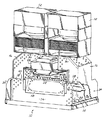
図面を参照すると、本発明の原理に従ったマイクロ波励起式の紫外線(UV)ランプシステム10が図示されている。紫外線ランプシステム10は、一対のマグネトロン12として示される一対のマイクロ波発生器を有している。該一対のマグネトロン12はそれぞれのウェーブガイド16を介して、長手的に延在するマイクロ波チャンバ14に連結されている。各ウェーブガイド16は、マイクロ波チャンバ14の上端部に連結される出口ポート18を有している。一対のマイクロ波発生器12が発生するマイクロ波エネルギーは、マイクロ波チャンバ14に対して、その両側上端部に隣接して長手方向に離間した位置において結合される。
当該技術において知られているように、密閉された細長く延在する管状の無電極プラズマバルブ20が、マイクロ波チャンバ14に設置され、且つマイクロ波チャンバ14の上面付近に支持されている。図示されていないが、以下のことを理解されたい。即ちランプシステム10は、当業者によく知られた、加圧空気源を含んだキャビネットまたはハウジング内に設置されており、該加圧空気源は、マイクロ波チャンバー14内にエアを向けるよう動作し、バルブ20を冷却する。
【0014】
ランプシステム10は、マグネトロン12からマイクロ波チャンバ14に結合された電磁波によるプラズマバルブ20内のガスの十分な励起によって、マイクロ波チャンバ14の底面から、図2中の矢印24によって概略示されるように、紫外線の放射を放つよう設計や構成がなされる。なおここでは一対のマグネトロン12を、図示し説明していくが、ランプシステム10は、単一のマグネトロン12を含んで、プラズマバルブ20内の混合ガスを励起させるようにしても、本発明の思想や範囲から外れることがないことを理解されたい。プラズマバルブ20内の混合ガスは、放出される放射の所定の波長分布を作り出すようにその元素を調整する。これらの目的のために都合のよい混合ガスは、水銀蒸気とアルゴンに鉄などの微量元素を加えたものである。バルブ20内の励起した混合ガスによって出力された電磁気の放射は、強い紫外線と赤外線の成分を含んでいる。ここでは、電磁放射(以下、放射と称する)は、約200nmから約1000nmにわたる波長として定義され、紫外線放射は、約200nmから約400nmにわたる波長として定義され、また赤外線放射は、約750nmから約1000nmにわたる波長として定義される。
【0015】
ランプシステム10は、一つのスタータバルブ26と、一対の変圧器28を備えている。これら変圧器28は、各マグネトロン12に電気的に接続されており、当業者に知られているようにマグネトロン12のフィラメントに電力供給する。マグネトロン12はウェーブガイド16の入り口ポート30に取り付けられており、マグネトロン12により発生されるマイクロ波はウェーブガイド16の長手方向に離間した出口ポート18を介してチャンバ14に放出される。好ましくは、2つのマグネトロン12の周波数をわずかに分離し(ずらし)、ランプシステムの動作中にそれらが相互結合(intercoupling)するのを防止する。本発明を限定するものではないが、具体的な例としては、2つのマグネトロン12は、それぞれ約2470MHzと約2445MHzの周波数で動作することができる。
【0016】
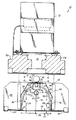
図1と図2を参照すれば、最もよく解るように、マイクロ波チャンバ14は、ほぼ水平な上面32と、ほぼ垂直な対向する一対の端壁34と、端壁34の間で長手方向に延び、且つプラズマバルブ20の両側に位置するほぼ垂直な対向する一対の側壁36とを有している。マイクロ波チャンバ14は、さらに側壁36から上面32に向かって上方に且つ内側に延在する傾いた傾壁38を有している。
一対の開口40が、マイクロ波チャンバ14の上端に設けられている。その開口40は、ウェーブガイド16の出口ポート18に整列されて(位置合わせされて)連結される。一対のマグネトロン12によって発生された電磁波は、マイクロ波チャンバ14に結合され、十分なエネルギーによってバルブ20内の混合ガスを励起し、これによりガス原子は多くの紫外線と赤外線の成分を有した放射のスペクトルを放出する。もちろん、本発明書の思想や範囲から外れることなくマイクロ波チャンバ14の他の形態も可能である。例えば、知られているように、放電によって混合ガスを励起するための電源に接続された電極をバルブ20の両端に内蔵してもよい。
【0017】
本発明の原理に従って、長手方向に延在する反射器42がマイクロ波チャンバ42内に設置されている。この反射器は図2に矢印21によって図式的に示されているプラズマバルブ20から発する放射のスペクトルから、紫外線放射を優先選択的に反射してマイクロ波チャンバ14の底面の下方に位置する基板(不図示)に向ける。メッシュ(網目)スクリーン44が、マイクロ波チャンバ14の底面に取り付けられている。メッシュスクリーン44は紫外線放射24は透過するが、一対のマグネトロン12によって発生されたマイクロ波は閉じこめる。網目スクリーン44は、高い導電性の金属、好ましくはタングステンからなり、且つ入射紫外線放射に対する高い透過率(好ましくは90%以上)を有している。
【0018】
図1および図2に示すように、反射器42はマイクロ波チャンバ14内に取り付けられた一対の長手方向に延在する反射パネル46を含んでいる。反射パネルはそれぞれ対向して向き合いかつプラズマバルブ20から離間した内側凹面43を有している。本発明書の思想や範囲から外れることなく、反射器42は、マイクロ波チャンバ内に延在しバルブ20から離間したワンピースの一体型パネル46または2枚以上からなるパネル46のどちらでもよいことはあきらかである。
【0019】
おのおのの内側面は、光学的に平坦な表面仕上げを有することが望ましく、おのおのの反射パネル46は、PYREX(登録商標)のような放射透過性の物質の層で構成されることが望ましい。適度な反射と温度の特性を有している他の物質(金属など)は、マイクロ波チャンバ14の一部に用いられ放射伝達が要求されない特定の用途に際して付随的に使用されるであろう。
【0020】
紫外線ランプシステム10を使用するために、反射器42は、プラズマバルブ20によって放射される放射21の特定の波長を少なくとも部分的に透過、反射もしくは吸収するように機能することができる。特に反射器は、図2の矢印22によって図式的に示されるように、赤外線を好適に透過し、且つ入射する放射21内の紫外線放射24は、反射する。従来知られているように、このような結果をもたらすためのよく知られている方法は、ダイクロイックコーティング(不図示)によって、おのおのの反射パネル46の内側面43をコートすることである。このダイクロイックコーティングは、通常屈折率の高低が交互にくる多様な誘電体の材料からなる周期的多層フィルムから構成される。このコーティングが非金属であるゆえに、一対のマグネトロン12から下方に向かって反射器42の裏面に入射するマイクロ波放射は、調節された層とほとんど干渉することなく、即ちほとんど吸収されることなく容易に透過され、バルブ20内の混合ガスをイオン化する。典型的なコーティングは「Balzers #UNS200-S 多層性コーティング」であり、これは波長220nm-440nmの入射放射に対して反射性が高い。
【0021】
図2に示すように、赤外線放射22は、反射器42を介して透過され、且つマイクロ波チャンバ14の周囲に導かれる。チャンバ壁32、34、36、38は、赤外線放射22を吸収したり、放散したりする。その結果、基板(不図示)は反射器42から反射される望ましくない間接赤外線放射22によってさらされることがない。あるいは代替的には、反射器42は、赤外線放射22を吸収するようにしてもよい。対照的に、紫外線放射24は、反射器42によってよく反射され、マイクロチャンバ14の底面より下の網目スクリーン44を越えて所定の距離に配置された基板に向けられる。
【0022】
一対の反射パネル46は、一対の長手方向に離間したリテーナ48(その内の一方のみが図2に示されている)によってマイクロ波チャンバ14内に取り付けられている。各反射パネル46は最下端部53を有しており、該最下端部53は各チャンバ側壁36から内側に延びる概して水平の内向きフランジ50上に支持されている。長手方向に延在する中間部材52がリテーナ48内に形成された一対のスロット54(図2)によってマイクロ波チャンバ内に取り付けられている。中間部材52は反射パネル46の各頂点55から離間して、かつプラズマバルブ20から離間して位置しており、バルブを冷却するのに十分な空気の循環を可能にする。この中間部材52はPYREX(登録商標)などのガラス製としてよく、またコーティングせずにバルブ20から放出される紫外線放射24に対して非反射性としてよい。
【0023】
本発明の一つの態様によれば、各反射パネル46の内面43は非2次の(non-quadratic)数学的関係式で定義される湾曲を有する非球面ミラーの一部を表している。説明のために図2に直交2次元デカルト座標系を定義しており、ここでは原点58をとり、パネルの内面43に垂直な平面内の各点を該原点58に対する座標(x,y)で表している。各パネル46はそれぞれの頂部56で切頭されており、かつその最下端53は式y=0で定義される平面から所定距離59だけ持ち上げられている。このデカルト座標系では各反射パネル46の内面43の湾曲は数学的関係式(x/a)(2+n)+(y/b)(2+m)=1で表される。なおここでbは曲線の半短径でありaは半長径である。
【0024】
反射器42の示す回転面を作り出すために、指数nおよびmをそれぞれ0.8に設定した。しかし指数nおよびmの値はこれには限定されず、約2より小さく0以上であってかつnおよびmの少なくとも一方は0より大となるような値とすることができる。好適には指数nおよびmの値を約0.7〜0.8の範囲に設定する。n=0かつm=0であれば、数学的関係式は通常の楕円となり、各パネル46は楕円柱の一部をなす形状となる。いずれのパネル46もマイクロ波チャンバの範囲内でx方向あるいはy方向にずらすことができ、それによって各内面43はプラズマバルブ20の周囲でもはや配置の対称性を失うが、このようなものも本発明の思想の範囲内に含まれるものであることを理解されたい。
【0025】
上記式で定義される湾曲面が長手方向に延在して反射器42を形成する。プラズマバルブ20の軸は反射器42の焦点あるいはその近傍に位置決めされ、プラズマバルブ20から放出される紫外線放射24は反射器42によってほとんどホモセントリックな平行光線として下方に反射され、メッシュスクリーン44を介して基板(不図示)に向けられる。数学的に表現された内面43の湾曲により、比較的均一な照射あるいは放射光束密度を有する紫外線放射24が基板の比較的大きな表面領域にわたってもたらされる。またこの均一な照射はマイクロ波チャンバの最適な寸法と干渉することなく達成される。
【0026】
本発明を限定するものではないが、例として示すと、反射器42の好適な実施例は切頭された頂部56までのy方向寸法が75.29mm(2.964インチ)であり、最下端部53までのx方向寸法が39.98mm(1.574インチ)である。なおこれらは原点58から各パネル46の内側凹面43までを計測したものである。また、この好適な実施例の反射器42のランプの軸に平行な長手方向寸法は251.00mm(9.882インチ)であり、その公称厚さは3.175mm(0.125インチ)である。更に、この好適な実施例の各パネル46の持ち上がり距離59は6.25mm(0.246インチ)であり、パネル46の頂部56は17.98mm(0.708インチ)の横方向隙間によって隔てられている。
【0027】
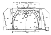
図1および図2と同じ参照符号を用いて、本発明の原理による反射器62の別の実施例を図3に示す。反射器62は一対の長く延びる反射パネル64を有している。これら反射パネルはマイクロ波チャンバ14内に各内側凹面66が互いに対向し対面するように、かつプラズマバルブ20から離間するように取り付けられている。各反射パネル64は上に反射パネル46に関連して説明した数学的関係式によって表現される好適な湾曲内側表面66を有している。反射器62を形成する指数nおよびmはそれぞれ0.7とした。一対の反射パネル64はリテーナ68によりマイクロ波チャンバ14内に取り付けられており、かつ各反射パネル64の最下端部70は、概して水平で各チャンバ側壁36から内側に延在するフランジ50上に支持されている。各パネル64はそれぞれの頂部72で切頭されており、またその最下端部70はx=0で定義される平面から上方に所定距離74だけ持ち上げられている。
【0028】
反射器62は反射器42(図1および図2)に関連して説明したものと同様に動作するものであり、比較的均一な紫外線放射の照射を基板の比較的広い表面領域に与え、その際マイクロ波チャンバの最適寸法と干渉することがない。
【0029】
本発明を限定するものではないが、例として示すと、反射器62の好適な実施例は切頭された頂部72までのy方向寸法が75.59mm(2.976インチ)であり、最下端部70までのx方向寸法が50.01mm(1.969インチ)である。なおこれらは原点58から各パネル64の内側凹面66までを計測したものである。また、この好適な実施例の反射器62のランプの軸に平行な長手方向寸法は146.99mm(5.787インチ)であり、その公称厚さは3.175mm(0.125インチ)である。更に、この好適な実施例の各パネル64の持ち上がり距離74は6.35mm(0.250インチ)であり、パネル64の頂部72は11.99mm(0.472インチ)の横方向隙間によって隔てられている。
【0030】
以上本発明を様々な実施形態により細部にわたって説明してきたが、特許請求の範囲に記載した本発明の範囲をこれらの細部によって限定しようと意図するものではない。その他の利点および変形例は当業者には容易に理解されるだろう。たとえば、本発明は反射器の焦点又はその付近に位置する放射源を有する任意の光反射システムにおいて基板その他の目標物の比較的広い表面にわたって比較的均一な照射をおこなうために用いることができる。したがって本発明を広くとらえれば、図示されかつ上に説明された特定の細部、代表的な装置および方法、そして例示のための実施例などに限定されるものではない。従って本発明の概括的思想の範囲を逸脱することなく、上記の細部からの変更を行うことができる。
【図面の簡単な説明】
【図1】本発明の原理による紫外線ランプシステムの斜視図である。
【図2】図1の紫外線ランプシステムの線2−2に沿った断面図であり、図1のランプシステムに用いる2つのパネルを有する反射器の位置実施形態を示す図である。
【図3】図1のランプ紫外線システムに用いる、本発明による2つのパネルを有する反射器の別の実施例を示す断面図である。
【符号の説明】
10………紫外線ランプシステム
12………マグネトロン
14………マイクロ波チャンバ
16………ウェーブガイド
18………出口ポート
20………プラズマバルブ
21………矢印
22………矢印
24………紫外線放射
26………スタータバルブ
28………変圧器
32………上面
34………端壁
36………側壁
38………傾壁
40………開口
42………反射器
43………内側凹面
44………メッシュスクリーン
46………反射器パネル
50………フランジ
53………最下端
56………頂部
58………原点
59………所定距離
59………持ち上がり距離
62………反射器
64………反射器パネル
66………内側凹面
68………リテーナ
70………最下端部
72………頂部
74………所定距離
74………持ち上がり距離[0001]
BACKGROUND OF THE INVENTION
The present invention generally relates to an ultraviolet lamp system, and more particularly to a reflector for reflecting ultraviolet radiation generated by a plasma bulb disposed in the system used in the ultraviolet lamp system.
[0002]
[Prior art]
The ultraviolet lamp system is adapted to couple the microwave energy to an electrodeless lamp such as an ultraviolet plasma bulb located in a microwave cavity or microwave chamber within the system. In ultraviolet thermosetting, the lamp system is provided with one or more magnetrons to couple microwave radiation to a plasma bulb in the microwave chamber. The magnetron is coupled to the microwave chamber via a waveguide having an output port connected to the upper end of the chamber. When the plasma bulb is sufficiently excited by microwave energy, it emits a radiation spectrum having strong ultraviolet and infrared components from the lower end of the microwave chamber toward the irradiation target substrate. In general, the ultraviolet lamp system also has a metal net provided at the lower end of the chamber that transmits ultraviolet rays but does not transmit microwaves generated by the magnetron. It should be understood that the “upper end” and “lower end” are used here to simplify the description of the microwave chamber in relation to the orientation of the chamber shown in the drawing. Of course, depending on the particular application of UV lamp heat curing, the orientation of the microwave chamber can be changed without any modification to the structure and function of the microwave chamber.
[0003]
Plasma bulbs (plasma bulbs or plasma bulbs) provide an approximate linear light source having a characteristic spectrum and emits radiation isotropically outward along its longitudinal direction. However, most of the emitted radiation reaches the substrate after one or more reflections. For example, UV lamp systems used to cure or heat adhesives, sealants, inks, coating materials, etc. include a reflector that is mounted in or forms part of a microwave chamber in which a plasma bulb is located. . A reflector is an optical element that functions to direct reflected radiation onto a substrate according to a predetermined pattern.
[0004]
In most UV lamp systems, cold-light illumination is desired. In cold light illumination, the infrared component of radiation emitted by the plasma bulb is removed by an absorption filter or a reflection filter in the system. Infrared radiation interacts with the substrate and heats the irradiated surface. Accordingly, the preferred reflector of such a system selectively reflects and transmits radiation as a function of wavelength. In particular, the reflector can be a coated optical element having a wavelength selective coating that preferentially directs UV light to the substrate. Wavelength selective coatings are generally multilayer thin films of dielectric materials, which are applied using vacuum deposition techniques such as physical vapor deposition or chemical vapor deposition well known to those skilled in the art. Radiation having wavelengths in the infrared region is transmitted by the reflector, absorbed by the surrounding structure and thermally dissipated. Thus, the extra infrared radiation is not substantially reflected by the reflector and does not illuminate the substrate.
[0005]
[Problems to be solved by the invention]
The reflector geometry determines the pattern of radiation that illuminates the substrate. The reflector is typically made in the shape of a part of a conic curve such as a parabola, ellipse, hyperbola, circle obtained by cutting a cone in a plane. In general, an elliptical reflector is used to provide a focused beam of ultraviolet radiation to a substrate placed at or near the focal point of the reflector. The characteristic of an elliptic reflector is that a light beam emitted from a light source located at one focal point of the ellipse is reflected once by the reflector and then passes through the other focal point. Thus, an elliptical reflector with a plasma bulb placed axially along one focal point will give focused linear radiation to a substrate located at the second focal point.
[0006]
On the other hand, some applications of ultraviolet lamp systems require uniform illumination or radiation density over a relatively large area of the substrate. For such applications, a hyperbolic reflector with a radiation source placed at the hyperbolic focus would be ideal. Indirect radiation emanating from such a linear light source of a hyperbolic reflector is reflected as a concentric collimated beam of light toward an infinite focal plane. However, since the hyperbolic reflector is relatively wide according to the mathematical description assigned to the hyperbolic surface, in most cases the hyperbolic reflector is physically unable to fit in the available space of most microwave chambers.
[0007]
In the past, attempts have been made to design UV lamp systems to provide uniform radiation by adjusting the reflector-plasma bulb-substrate optical arrangement. One solution that has been proposed to provide a smaller reflector has been to reposition the plasma bulb away from the focal point of the elliptical reflector. Although the ultraviolet radiation reflected by this configuration was at least partially defocused, the irradiation was not sufficiently uniform across the substrate surface. Furthermore, the coupling between the incident microwave energy and the gas in the plasma bulb changes, and the irradiation becomes non-uniform along the length of the plasma bulb. Another proposed solution is to change the position of the elliptical reflector so that the substrate is not located at or near the focal plane. However, the repositioning of the reflector reduces the cooling that can be applied to the plasma bulb, thereby reducing the useful life of the plasma bulb.
[0008]
Reflections designed to efficiently provide uniform UV radiation over a large area and do not interfere with the optimum dimensions of the microwave chamber or adversely affect the operating characteristics of the plasma bulb. A vessel is required.
[0009]
[Means for Solving the Problems]
The present invention overcomes these and other disadvantages of currently known microwave-excited ultraviolet lamp systems. The present invention will be described later in connection with certain embodiments, but the present invention is not limited to these embodiments. On the contrary, the invention is intended to cover all alternative constructions, modifications, and equivalents that may be included within the spirit and scope of the invention.
[0010]
The reflector according to the present invention comprises one or more longitudinally extending reflective panels adapted to be spaced from the plasma bulb of the ultraviolet lamp system. The reflector reflects the electromagnetic radiation emitted by the plasma bulb, particularly ultraviolet radiation, and can provide a substantially uniform illumination on the surface of the adjacent substrate. The curvature of the main part of each reflective panel is expressed by the equation (x / a) (2 + n) + (y / b) (2 + m) = 1 in Cartesian coordinates. Here, a and b are constants, n and m are indices less than about 2 and greater than or equal to 0, and at least one of n or m is greater than 0.
[0011]
This curvature of the reflector results in the irradiation of substantially uniform UV radiation over a large area. In addition, the reflector does not interfere with the optimum dimensions of the microwave chamber and does not adversely affect the operating characteristics of the plasma bulb. Furthermore, this reflector is suitable for the available space of the microwave chamber.
[0012]
The objects and advantages of the present invention described above will be apparent from the accompanying drawings and the description thereof.
[0013]
DETAILED DESCRIPTION OF THE INVENTION
Referring to the drawings, a microwave-excited ultraviolet (UV)
As is known in the art, a sealed elongate tubular
[0014]
The
[0015]
The
[0016]
With reference to FIGS. 1 and 2, as best seen, the
A pair of openings 40 is provided at the upper end of the
[0017]
In accordance with the principles of the present invention, a
[0018]
As shown in FIGS. 1 and 2, the
[0019]
Each inner surface preferably has an optically flat surface finish, and each reflective panel 46 is preferably composed of a layer of radiation transmissive material such as PYREX®. Other materials (such as metals) that have reasonable reflection and temperature characteristics may be used incidentally in certain applications that are used in a portion of the
[0020]
In order to use the
[0021]
As shown in FIG. 2, the infrared radiation 22 is transmitted through the
[0022]
The pair of reflective panels 46 are mounted in the
[0023]
According to one aspect of the present invention, the
[0024]
In order to create the rotating surface indicated by the
[0025]
The curved surface defined by the above formula extends in the longitudinal direction to form the
[0026]
By way of example, but not by way of limitation, the preferred embodiment of the
[0027]
Another embodiment of a
[0028]
The
[0029]
By way of example, and not by way of limitation, the preferred embodiment of the
[0030]
While the invention has been described in detail through various embodiments, it is not intended that the scope of the invention described in the claims be limited by these details. Other advantages and modifications will be readily apparent to those skilled in the art. For example, the present invention can be used to provide relatively uniform illumination over a relatively large surface of a substrate or other target in any light reflecting system having a radiation source located at or near the focal point of the reflector. Accordingly, the present invention is not broadly limited to the specific details, representative apparatus and methods, illustrative examples, and the like illustrated and described above. Accordingly, changes from the above details may be made without departing from the scope of the general idea of the invention.
[Brief description of the drawings]
FIG. 1 is a perspective view of an ultraviolet lamp system according to the principles of the present invention.
2 is a cross-sectional view of the UV lamp system of FIG. 1 taken along line 2-2 showing a position embodiment of a reflector having two panels for use in the lamp system of FIG.
FIG. 3 is a cross-sectional view showing another embodiment of a reflector having two panels according to the present invention for use in the lamp ultraviolet system of FIG.
[Explanation of symbols]
10 .........
Claims (16)
(x/a)(2+n) + (y/b)(2+m) = 1
ここで、aおよびbは定数、nおよびmは約2より小さく0以上の指数であり、nおよびmの少なくとも一方は0より大である。 A reflector for providing a relatively uniform illumination over a relatively large surface area of a target located below a lamp system, used in a lamp system having an elongated bulb for emitting a spectrum of radiation , The reflector is arranged so as to be spaced apart from the elongated bulb, and the curvature of the main part of the reflector is represented by the following formula in a Cartesian coordinate system:
(x / a) (2 + n) + (y / b) (2 + m) = 1
Here, a and b are constants, n and m are indices less than about 2 and greater than or equal to 0, and at least one of n and m is greater than 0.
バルブから離間して取り付けられるようになされた第1の長手に延在する反射パネルと、
バルブから離間すると共に前記第1の反射パネルと対向して取り付けられるようになされた第2の長手に延在する反射パネルと、
を有することを特徴とする請求項1記載の反射器。The reflector is
A first longitudinally extending reflective panel adapted to be mounted remotely from the bulb;
A second longitudinally extending reflective panel spaced apart from the bulb and adapted to be mounted opposite the first reflective panel;
The reflector according to claim 1, comprising:
細長く延びるマイクロ波チャンバと、
前記マイクロ波チャンバ内に設置された細長く延びるバルブと、
前記マイクロ波チャンバに結合され、前記チャンバ内にマイクロ波エネルギー場を発生可能であり、前記バルブを励起して電磁放射を放出させる少なくとも一つのマイクロ波発生器と、
細長く延びるバルブから離間して設置されるようになされた反射器と、
を有し、該反射器の主要部分の湾曲はデカルト座標系において以下の式により表されることを特徴とする装置:
(x/a)(2+n) + (y/b)(2+m) = 1
ここで、aおよびbは定数、nおよびmは約2より小さく0以上の指数であり、nおよびmの少なくとも一方は0より大である。A device for generating ultraviolet radiation,
An elongated microwave chamber;
An elongated valve installed in the microwave chamber;
At least one microwave generator coupled to the microwave chamber, capable of generating a microwave energy field in the chamber, and exciting the valve to emit electromagnetic radiation;
A reflector adapted to be placed away from the elongated bulb;
And the curvature of the main part of the reflector is represented by the following formula in a Cartesian coordinate system:
(x / a) (2 + n) + (y / b) (2 + m) = 1
Here, a and b are constants, n and m are indices less than about 2 and greater than or equal to 0, and at least one of n and m is greater than 0.
バルブから離間して取り付けられるようになされた第1の長手に延在する反射パネルと、
バルブから離間すると共に前記第1の反射パネルと対向して取り付けられるようになされた第2の長手に延在する反射パネルと、
を有することを特徴とする請求項8記載の装置。The reflector is
A first longitudinally extending reflective panel adapted to be mounted remotely from the bulb;
A second longitudinally extending reflective panel spaced apart from the bulb and adapted to be mounted opposite the first reflective panel;
9. The apparatus of claim 8, comprising:
長手軸を有するバルブと、
前記バルブに作動的に結合され、該バルブを励起して電磁放射を放出させるパワー供給源と、
長手方向に延びるバルブから離間して設置された反射器と、
を有し、該反射器の主要部分の湾曲はデカルト座標系において以下の式により表されることを特徴とする装置:
(x/a)(2+n) + (y/b)(2+m) = 1
ここで、aおよびbは定数、nおよびmは約2より小さく0以上の指数であり、nおよびmの少なくとも一方は0より大である。An apparatus for generating substantially uniform radiation over a relatively large surface area of a target,
A valve having a longitudinal axis;
A power source operatively coupled to the valve to excite the valve to emit electromagnetic radiation;
A reflector placed away from the longitudinally extending bulb;
And the curvature of the main part of the reflector is represented by the following formula in a Cartesian coordinate system:
(x / a) (2 + n) + (y / b) (2 + m) = 1
Here, a and b are constants, n and m are indices less than about 2 and greater than or equal to 0, and at least one of n and m is greater than 0.
Applications Claiming Priority (2)
| Application Number | Priority Date | Filing Date | Title |
|---|---|---|---|
| US09/659,075 US6323601B1 (en) | 2000-09-11 | 2000-09-11 | Reflector for an ultraviolet lamp system |
| US09/659075 | 2000-09-11 |
Publications (2)
| Publication Number | Publication Date |
|---|---|
| JP2002175711A JP2002175711A (en) | 2002-06-21 |
| JP4982015B2 true JP4982015B2 (en) | 2012-07-25 |
Family
ID=24643925
Family Applications (1)
| Application Number | Title | Priority Date | Filing Date |
|---|---|---|---|
| JP2001274905A Expired - Fee Related JP4982015B2 (en) | 2000-09-11 | 2001-09-11 | Reflector for UV lamp system |
Country Status (4)
| Country | Link |
|---|---|
| US (1) | US6323601B1 (en) |
| EP (1) | EP1186913A3 (en) |
| JP (1) | JP4982015B2 (en) |
| CN (1) | CN1184432C (en) |
Families Citing this family (45)
| Publication number | Priority date | Publication date | Assignee | Title |
|---|---|---|---|---|
| DE20004368U1 (en) * | 2000-03-10 | 2000-10-19 | Heraeus Noblelight Gmbh, 63450 Hanau | Electrodeless discharge lamp |
| US6471376B1 (en) * | 2000-08-17 | 2002-10-29 | General Electric Company | Increased life reflector lamps |
| AUPR214500A0 (en) * | 2000-12-18 | 2001-01-25 | Barry Webb & Associates, (NSW) Pty Limited | A light reflector |
| US20020079796A1 (en) * | 2000-12-22 | 2002-06-27 | Okamitsu Jeffrey K. | Wavelength selective optical reflector with integral light trap |
| US6646384B2 (en) * | 2002-02-20 | 2003-11-11 | Fusion Uv Systems, Inc. | Microwave powered UV lamp with improved RF gasket arrangement |
| US6797971B2 (en) * | 2002-07-18 | 2004-09-28 | Fusion Uv Systems, Inc. | Apparatus and method providing substantially two-dimensionally uniform irradiation |
| WO2004096527A2 (en) | 2003-05-01 | 2004-11-11 | Objet Geometries Ltd. | Rapid prototyping apparatus |
| IL157229A (en) * | 2003-08-04 | 2006-08-20 | Zamir Tribelsky | Method for energy coupling especially useful for disinfecting and various systems using it |
| US6905230B2 (en) * | 2003-08-18 | 2005-06-14 | Nordson Corporation | UV lamp retainer system |
| US6841790B1 (en) * | 2003-10-07 | 2005-01-11 | Miltec Corporation | Snap-in radio frequency screen for ultraviolet lamp system |
| US7109669B2 (en) * | 2004-04-08 | 2006-09-19 | Nordson Corporation | Microwave lamp power supply that can withstand failure in high voltage circuit |
| US20050250346A1 (en) * | 2004-05-06 | 2005-11-10 | Applied Materials, Inc. | Process and apparatus for post deposition treatment of low k dielectric materials |
| US7077547B2 (en) * | 2004-07-29 | 2006-07-18 | Nordson Corporation | Shuttered lamp assembly and method of cooling the lamp assembly |
| US7777198B2 (en) | 2005-05-09 | 2010-08-17 | Applied Materials, Inc. | Apparatus and method for exposing a substrate to a rotating irradiance pattern of UV radiation |
| US20060249175A1 (en) * | 2005-05-09 | 2006-11-09 | Applied Materials, Inc. | High efficiency UV curing system |
| US20060251827A1 (en) * | 2005-05-09 | 2006-11-09 | Applied Materials, Inc. | Tandem uv chamber for curing dielectric materials |
| JP2007026921A (en) * | 2005-07-19 | 2007-02-01 | Koito Mfg Co Ltd | Discharge bulb for automobile |
| US7566891B2 (en) * | 2006-03-17 | 2009-07-28 | Applied Materials, Inc. | Apparatus and method for treating a substrate with UV radiation using primary and secondary reflectors |
| US7692171B2 (en) * | 2006-03-17 | 2010-04-06 | Andrzei Kaszuba | Apparatus and method for exposing a substrate to UV radiation using asymmetric reflectors |
| US7589336B2 (en) * | 2006-03-17 | 2009-09-15 | Applied Materials, Inc. | Apparatus and method for exposing a substrate to UV radiation while monitoring deterioration of the UV source and reflectors |
| DE102006051738B4 (en) * | 2006-10-30 | 2012-12-20 | Heraeus Noblelight Gmbh | Packaging material sterilizing |
| GB0624075D0 (en) * | 2006-12-01 | 2007-01-10 | Gew Ec Ltd | a reflector |
| US7952289B2 (en) * | 2007-12-21 | 2011-05-31 | Nordson Corporation | UV lamp system and associated method with improved magnetron control |
| US7906911B2 (en) * | 2008-05-01 | 2011-03-15 | Fusion Uv Systems, Inc. | Luminaire assembly having a bonded reflector cavity for supporting an ultra-violet lamp |
| US8179046B2 (en) * | 2008-05-20 | 2012-05-15 | Nordson Corporation | Ultraviolet lamp system with cooling air filter |
| DE102008031996A1 (en) * | 2008-07-07 | 2010-02-18 | Osram Gesellschaft mit beschränkter Haftung | Radiation-emitting device |
| WO2010066298A1 (en) * | 2008-12-11 | 2010-06-17 | Osram Gesellschaft mit beschränkter Haftung | Uv light having a plurality of uv lamps, particularly for technical product processing |
| US8282435B2 (en) * | 2009-03-09 | 2012-10-09 | Topanga Technologies, Inc. | Method and system for replacing a plasma lamp from a resonator assembly |
| US8629616B2 (en) | 2011-01-11 | 2014-01-14 | Topanga Technologies, Inc. | Arc tube device and stem structure for electrodeless plasma lamp |
| US9177779B1 (en) | 2009-06-15 | 2015-11-03 | Topanga Usa, Inc. | Low profile electrodeless lamps with an externally-grounded probe |
| EP2827360A1 (en) * | 2010-03-22 | 2015-01-21 | Robe Lighting, Inc | Plasma light source automated luminaire |
| US9439273B2 (en) | 2010-07-12 | 2016-09-06 | Nordson Corporation | Ultraviolet lamp system and method for controlling emitted ultraviolet light |
| US20120258259A1 (en) | 2011-04-08 | 2012-10-11 | Amit Bansal | Apparatus and method for uv treatment, chemical treatment, and deposition |
| US9097577B2 (en) * | 2011-06-29 | 2015-08-04 | KLA—Tencor Corporation | Adaptive optics for compensating aberrations in light-sustained plasma cells |
| GB201206556D0 (en) * | 2012-04-13 | 2012-05-30 | Ceravision Ltd | Light source |
| US9171747B2 (en) | 2013-04-10 | 2015-10-27 | Nordson Corporation | Method and apparatus for irradiating a semi-conductor wafer with ultraviolet light |
| US9099291B2 (en) | 2013-06-03 | 2015-08-04 | Topanga Usa, Inc. | Impedance tuning of an electrode-less plasma lamp |
| KR102302122B1 (en) * | 2013-09-11 | 2021-09-13 | 헤라우스 노블라이트 아메리카 엘엘씨 | Large area high-uniformity uv source with many small emitters |
| US9392752B2 (en) | 2014-05-13 | 2016-07-19 | Topanga Usa, Inc. | Plasma growth lamp for horticulture |
| CN106838827A (en) * | 2017-01-18 | 2017-06-13 | 深圳市润沃自动化工程有限公司 | A kind of line source part curing of remote projection |
| US10265428B1 (en) | 2017-10-06 | 2019-04-23 | The Boeing Company | Reflector system for a lighting assembly |
| EP3986607A4 (en) | 2019-06-24 | 2023-05-10 | The University of British Columbia | MULTIPLE REFLECTOR PHOTOREACTOR FOR CONTROLLED FLUID IRRADIATION |
| EP4131655B1 (en) * | 2020-03-31 | 2025-11-19 | Agc Inc. | Wireless transmission system |
| CN120103675A (en) * | 2023-12-06 | 2025-06-06 | 拓荆创益(沈阳)半导体设备有限公司 | Light emitting unit and substrate processing device containing the same |
| US20260031316A1 (en) * | 2024-07-26 | 2026-01-29 | Excelitas Technologies Corp. | Method and apparatus for light generation |
Family Cites Families (15)
| Publication number | Priority date | Publication date | Assignee | Title |
|---|---|---|---|---|
| DE217720C (en) * | ||||
| US3398272A (en) * | 1965-12-03 | 1968-08-20 | William B. Elmer | Isoradiant energy reflecting |
| US4027151A (en) * | 1975-11-18 | 1977-05-31 | Crouse-Hinds Company | Luminaire and reflector therefor |
| US4042850A (en) | 1976-03-17 | 1977-08-16 | Fusion Systems Corporation | Microwave generated radiation apparatus |
| US4355350A (en) * | 1980-09-02 | 1982-10-19 | Polaroid Corporation | Reflector for use in an artificial lighting device |
| US4535753A (en) | 1984-04-12 | 1985-08-20 | Leo Zayauskas | Radiant heat collector |
| JPS614153A (en) * | 1984-06-14 | 1986-01-10 | フュージョン・システムズ・コーポレーション | Electrodeless lamp bulb and method of altering same |
| JPS62105303A (en) * | 1985-10-31 | 1987-05-15 | 三菱電機株式会社 | Lighting fixture |
| JPH0621167Y2 (en) | 1987-08-07 | 1994-06-01 | 高橋 柾弘 | Ultraviolet generator by microwave excitation |
| JPH0637521Y2 (en) | 1988-10-05 | 1994-09-28 | 高橋 柾弘 | Ultraviolet generator by microwave excitation |
| DE3919334A1 (en) | 1989-06-13 | 1990-12-20 | Tetsuhiro Kano | REFLECTOR FOR A LAMP |
| US5237170A (en) * | 1991-07-03 | 1993-08-17 | Shatz Narkis E I | Method and apparatus for non-imaging concentration and projection of electromagnetic radiation |
| US5586013A (en) * | 1991-07-19 | 1996-12-17 | Minnesota Mining And Manufacturing Company | Nonimaging optical illumination system |
| US5980067A (en) * | 1996-09-18 | 1999-11-09 | Valeo Vision | Indicator light for a motor vehicle, having a faceted reflector |
| US6118130A (en) * | 1998-11-18 | 2000-09-12 | Fusion Uv Systems, Inc. | Extendable focal length lamp |
-
2000
- 2000-09-11 US US09/659,075 patent/US6323601B1/en not_active Expired - Fee Related
-
2001
- 2001-09-01 EP EP01121037A patent/EP1186913A3/en not_active Withdrawn
- 2001-09-11 JP JP2001274905A patent/JP4982015B2/en not_active Expired - Fee Related
- 2001-09-11 CN CNB011421002A patent/CN1184432C/en not_active Expired - Fee Related
Also Published As
| Publication number | Publication date |
|---|---|
| US6323601B1 (en) | 2001-11-27 |
| CN1184432C (en) | 2005-01-12 |
| JP2002175711A (en) | 2002-06-21 |
| EP1186913A3 (en) | 2005-01-26 |
| CN1343852A (en) | 2002-04-10 |
| EP1186913A2 (en) | 2002-03-13 |
Similar Documents
| Publication | Publication Date | Title |
|---|---|---|
| JP4982015B2 (en) | Reflector for UV lamp system | |
| JP4777582B2 (en) | Microwave-excited UV lamp system with improved lamp cooling. | |
| US6657206B2 (en) | Ultraviolet lamp system and methods | |
| EP0450131B1 (en) | Electrodeless microwave-generated radiation apparatus | |
| US20050286263A1 (en) | Plasma lamp with light-transmissive waveguide | |
| JPH11503263A (en) | A device for exciting electrodeless lamps with microwave radiation | |
| US20050115498A1 (en) | Reflector for UV curing systems | |
| JP2001085152A (en) | Microwave device containing mesh member | |
| EP1151640A1 (en) | Extendable focal length lamp | |
| WO1999053524A1 (en) | Rf/microwave energised plasma light source | |
| JP4901041B2 (en) | Apparatus and method for generating ultraviolet light | |
| US6351070B1 (en) | Lamp with self-constricting plasma light source | |
| JP2011091007A (en) | Electrodeless lamp and ultraviolet irradiation device | |
| CN1855356B (en) | Plasma lighting system | |
| JPS61261055A (en) | Ultraviolet ray irradiation device | |
| US20020079796A1 (en) | Wavelength selective optical reflector with integral light trap | |
| JP2011113791A (en) | Metal halide lamp, ultraviolet irradiation device | |
| KR20070117386A (en) | Lighting equipment using microwave and its resonator | |
| JP2915181B2 (en) | Microwave electrodeless light emitting device | |
| JP2008053014A (en) | Light irradiation device | |
| US10008379B1 (en) | Infrared recycling incandescent light bulb | |
| JPS5923613B2 (en) | High frequency discharge light source device | |
| KR100430012B1 (en) | Preventive apparatus of heat transformation in plasma lighting system | |
| JPH05156050A (en) | Electrode UV lamp light emitting device | |
| JPS61281452A (en) | Microwave discharge light source |
Legal Events
| Date | Code | Title | Description |
|---|---|---|---|
| A621 | Written request for application examination |
Free format text: JAPANESE INTERMEDIATE CODE: A621 Effective date: 20080909 |
|
| A977 | Report on retrieval |
Free format text: JAPANESE INTERMEDIATE CODE: A971007 Effective date: 20110418 |
|
| A131 | Notification of reasons for refusal |
Free format text: JAPANESE INTERMEDIATE CODE: A131 Effective date: 20110425 |
|
| A601 | Written request for extension of time |
Free format text: JAPANESE INTERMEDIATE CODE: A601 Effective date: 20110725 |
|
| A602 | Written permission of extension of time |
Free format text: JAPANESE INTERMEDIATE CODE: A602 Effective date: 20110728 |
|
| A521 | Written amendment |
Free format text: JAPANESE INTERMEDIATE CODE: A523 Effective date: 20111014 |
|
| RD02 | Notification of acceptance of power of attorney |
Free format text: JAPANESE INTERMEDIATE CODE: A7422 Effective date: 20111014 |
|
| TRDD | Decision of grant or rejection written | ||
| A01 | Written decision to grant a patent or to grant a registration (utility model) |
Free format text: JAPANESE INTERMEDIATE CODE: A01 Effective date: 20120326 |
|
| A01 | Written decision to grant a patent or to grant a registration (utility model) |
Free format text: JAPANESE INTERMEDIATE CODE: A01 |
|
| A61 | First payment of annual fees (during grant procedure) |
Free format text: JAPANESE INTERMEDIATE CODE: A61 Effective date: 20120423 |
|
| FPAY | Renewal fee payment (event date is renewal date of database) |
Free format text: PAYMENT UNTIL: 20150427 Year of fee payment: 3 |
|
| R150 | Certificate of patent or registration of utility model |
Free format text: JAPANESE INTERMEDIATE CODE: R150 |
|
| LAPS | Cancellation because of no payment of annual fees |