JP4982469B2 - Optical module - Google Patents
Optical module Download PDFInfo
- Publication number
- JP4982469B2 JP4982469B2 JP2008280697A JP2008280697A JP4982469B2 JP 4982469 B2 JP4982469 B2 JP 4982469B2 JP 2008280697 A JP2008280697 A JP 2008280697A JP 2008280697 A JP2008280697 A JP 2008280697A JP 4982469 B2 JP4982469 B2 JP 4982469B2
- Authority
- JP
- Japan
- Prior art keywords
- light
- optical module
- optical
- emitting element
- light emitting
- Prior art date
- Legal status (The legal status is an assumption and is not a legal conclusion. Google has not performed a legal analysis and makes no representation as to the accuracy of the status listed.)
- Expired - Fee Related
Links
Images



Classifications
-
- G—PHYSICS
- G02—OPTICS
- G02B—OPTICAL ELEMENTS, SYSTEMS OR APPARATUS
- G02B6/00—Light guides; Structural details of arrangements comprising light guides and other optical elements, e.g. couplings
- G02B6/24—Coupling light guides
- G02B6/42—Coupling light guides with opto-electronic elements
- G02B6/4201—Packages, e.g. shape, construction, internal or external details
- G02B6/4246—Bidirectionally operating package structures
-
- G—PHYSICS
- G02—OPTICS
- G02B—OPTICAL ELEMENTS, SYSTEMS OR APPARATUS
- G02B6/00—Light guides; Structural details of arrangements comprising light guides and other optical elements, e.g. couplings
- G02B6/24—Coupling light guides
- G02B6/26—Optical coupling means
- G02B6/28—Optical coupling means having data bus means, i.e. plural waveguides interconnected and providing an inherently bidirectional system by mixing and splitting signals
- G02B6/293—Optical coupling means having data bus means, i.e. plural waveguides interconnected and providing an inherently bidirectional system by mixing and splitting signals with wavelength selective means
- G02B6/29346—Optical coupling means having data bus means, i.e. plural waveguides interconnected and providing an inherently bidirectional system by mixing and splitting signals with wavelength selective means operating by wave or beam interference
- G02B6/29361—Interference filters, e.g. multilayer coatings, thin film filters, dichroic splitters or mirrors based on multilayers, WDM filters
- G02B6/29362—Serial cascade of filters or filtering operations, e.g. for a large number of channels
- G02B6/29365—Serial cascade of filters or filtering operations, e.g. for a large number of channels in a multireflection configuration, i.e. beam following a zigzag path between filters or filtering operations
- G02B6/29367—Zigzag path within a transparent optical block, e.g. filter deposited on an etalon, glass plate, wedge acting as a stable spacer
-
- H—ELECTRICITY
- H01—ELECTRIC ELEMENTS
- H01S—DEVICES USING THE PROCESS OF LIGHT AMPLIFICATION BY STIMULATED EMISSION OF RADIATION [LASER] TO AMPLIFY OR GENERATE LIGHT; DEVICES USING STIMULATED EMISSION OF ELECTROMAGNETIC RADIATION IN WAVE RANGES OTHER THAN OPTICAL
- H01S2301/00—Functional characteristics
- H01S2301/17—Semiconductor lasers comprising special layers
- H01S2301/176—Specific passivation layers on surfaces other than the emission facet
-
- H—ELECTRICITY
- H01—ELECTRIC ELEMENTS
- H01S—DEVICES USING THE PROCESS OF LIGHT AMPLIFICATION BY STIMULATED EMISSION OF RADIATION [LASER] TO AMPLIFY OR GENERATE LIGHT; DEVICES USING STIMULATED EMISSION OF ELECTROMAGNETIC RADIATION IN WAVE RANGES OTHER THAN OPTICAL
- H01S5/00—Semiconductor lasers
- H01S5/005—Optical components external to the laser cavity, specially adapted therefor, e.g. for homogenisation or merging of the beams or for manipulating laser pulses, e.g. pulse shaping
-
- H—ELECTRICITY
- H01—ELECTRIC ELEMENTS
- H01S—DEVICES USING THE PROCESS OF LIGHT AMPLIFICATION BY STIMULATED EMISSION OF RADIATION [LASER] TO AMPLIFY OR GENERATE LIGHT; DEVICES USING STIMULATED EMISSION OF ELECTROMAGNETIC RADIATION IN WAVE RANGES OTHER THAN OPTICAL
- H01S5/00—Semiconductor lasers
- H01S5/02—Structural details or components not essential to laser action
- H01S5/022—Mountings; Housings
- H01S5/02208—Mountings; Housings characterised by the shape of the housings
- H01S5/02212—Can-type, e.g. TO-CAN housings with emission along or parallel to symmetry axis
-
- H—ELECTRICITY
- H01—ELECTRIC ELEMENTS
- H01S—DEVICES USING THE PROCESS OF LIGHT AMPLIFICATION BY STIMULATED EMISSION OF RADIATION [LASER] TO AMPLIFY OR GENERATE LIGHT; DEVICES USING STIMULATED EMISSION OF ELECTROMAGNETIC RADIATION IN WAVE RANGES OTHER THAN OPTICAL
- H01S5/00—Semiconductor lasers
- H01S5/02—Structural details or components not essential to laser action
- H01S5/022—Mountings; Housings
- H01S5/02218—Material of the housings; Filling of the housings
- H01S5/02234—Resin-filled housings; the housings being made of resin
-
- H—ELECTRICITY
- H01—ELECTRIC ELEMENTS
- H01S—DEVICES USING THE PROCESS OF LIGHT AMPLIFICATION BY STIMULATED EMISSION OF RADIATION [LASER] TO AMPLIFY OR GENERATE LIGHT; DEVICES USING STIMULATED EMISSION OF ELECTROMAGNETIC RADIATION IN WAVE RANGES OTHER THAN OPTICAL
- H01S5/00—Semiconductor lasers
- H01S5/02—Structural details or components not essential to laser action
- H01S5/022—Mountings; Housings
- H01S5/0225—Out-coupling of light
- H01S5/02251—Out-coupling of light using optical fibres
-
- H—ELECTRICITY
- H01—ELECTRIC ELEMENTS
- H01S—DEVICES USING THE PROCESS OF LIGHT AMPLIFICATION BY STIMULATED EMISSION OF RADIATION [LASER] TO AMPLIFY OR GENERATE LIGHT; DEVICES USING STIMULATED EMISSION OF ELECTROMAGNETIC RADIATION IN WAVE RANGES OTHER THAN OPTICAL
- H01S5/00—Semiconductor lasers
- H01S5/02—Structural details or components not essential to laser action
- H01S5/022—Mountings; Housings
- H01S5/0225—Out-coupling of light
- H01S5/02257—Out-coupling of light using windows, e.g. specially adapted for back-reflecting light to a detector inside the housing
Landscapes
- Physics & Mathematics (AREA)
- General Physics & Mathematics (AREA)
- Optics & Photonics (AREA)
- Optical Couplings Of Light Guides (AREA)
- Semiconductor Lasers (AREA)
Description
本発明は、同一筐体内に発光素子と受光素子を搭載する光モジュールにおいて、光クロストークを抑制する構造を有する光モジュールに関するものである。 The present invention relates to an optical module having a structure for suppressing optical crosstalk in an optical module in which a light emitting element and a light receiving element are mounted in the same housing.
光送受信モジュール等の発光素子(半導体レーザ)と受光素子(フォトダイオード)を同一筐体内に備える光モジュールにおいて、光クロストークを抑制することは良好な受光感度を得るうえで極めて重要な要素となっている。この光クロストークの原因としては主に以下の2つの経路が存在している。第1の経路は、発光素子から出射した光が筐体の内壁で散乱され、受光素子に達するものである。第2の経路は、発光素子(半導体レーザ)の活性層から基板内に漏れ出た光(以下、漏れ光と記す。)が発光素子の側面から外部へ出射され、直接もしくは筐体の内壁で散乱され、受光素子に達するものである。これら光クロストークを抑制するために、従来から様々な手法が考案されてきた。 In an optical module having a light emitting element (semiconductor laser) and a light receiving element (photodiode) such as an optical transceiver module in the same housing, suppressing optical crosstalk is an extremely important factor for obtaining good light receiving sensitivity. ing. There are mainly the following two paths as the cause of this optical crosstalk. In the first path, light emitted from the light emitting element is scattered by the inner wall of the housing and reaches the light receiving element. In the second path, light leaked from the active layer of the light emitting element (semiconductor laser) into the substrate (hereinafter referred to as leaked light) is emitted to the outside from the side surface of the light emitting element and directly or on the inner wall of the housing. It is scattered and reaches the light receiving element. In order to suppress these optical crosstalks, various methods have been devised.
例えば、特許文献1では、基板上に発光素子と受光素子を搭載した光モジュールにおいて、該発光素子と受光素子間に波長選択フィルタを挿入し、発光素子からの迷光を反射させることにより光クロストークを抑制する光モジュールが記載されている。
For example, in
また、特許文献2および特許文献3には、基板上に複数の光半導体素子を搭載した光モジュールにおいて、その複数の光半導体素子の間に光吸収樹脂(または遮光樹脂)を配置することにより、該素子間の光クロストークを抑制する構造をとっており、前記光吸収樹脂(または遮光樹脂)は、前記光半導体素子の周囲を透明樹脂で覆った上から、該透明樹脂を含めて基板表面に塗布されている光モジュールが記載されている。
Further, in
特許文献1では、発光素子と受光素子間に波長選択フィルタが挿入された形態であるため、発光素子から受光素子へ直接入射する光に関しては、遮断することができる。しかしながら、発光素子の後方(波長選択フィルタと反対側)へ出射した光(漏れ光)が筐体の内壁で散乱し、受光素子に入射する経路(上記第2の経路)に対して、波長選択フィルタは有効に機能しない構成となっている。換言すると、漏れ光(上記第2の経路)起因の光クロストークを抑制できない構成となっている。
In
特許文献2および特許文献3では、上記漏れ光(上記第2の経路)起因の光クロストークの抑制を考慮して、樹脂が発光素子を完全に覆い、且つ樹脂と基板が接着した形態となっている。しかしながら、この形態では樹脂と基板が接着しているため、樹脂の熱収縮により発光素子に歪みが発生する。換言すると、発光素子内の回折格子の間隔が変化することとなる。この回折格子間隔の変化は、発光波長の変動を引き起こす虞がある。また、歪みにより発光素子の信頼性低下が懸念される。さらに、特許文献2および特許文献3では、樹脂で吸収(遮断)しきれなかった漏れ光が、光クロストークを引き起こす原因となり得る可能性がある構成となっている。
In
以上述べたように、発光素子と受光素子が同一筐体内に備える光モジュールにおいて、従来の技術では発光素子の特性劣化、信頼性低下を引き起こすことなく漏れ光(第2の経路)による光クロストークを抑制することが困難であった。 As described above, in an optical module in which a light emitting element and a light receiving element are provided in the same casing, optical crosstalk due to leaked light (second path) without causing deterioration of characteristics and reliability of the light emitting element in the conventional technology. It was difficult to suppress.
本発明の目的は上記を鑑み、簡便な構造で発光素子の特性劣化、信頼性低下を引き起こすことなく漏れ光起因の光クロストークを抑制し、良好な受光感度を得ることのできる光モジュールを提供することにある。 SUMMARY OF THE INVENTION In view of the above, an object of the present invention is to provide an optical module capable of suppressing light crosstalk caused by leaked light and obtaining good light receiving sensitivity without causing deterioration in characteristics and reliability of a light emitting element with a simple structure. There is to do.
上記課題を解決するため、下記のいずれかの特徴を有する。 In order to solve the above-mentioned problems, it has any of the following features.
本発明では光素子(発光素子および受光素子)を搭載する基板上に樹脂と非接着な材質を形成した領域を設ける。さらに、光吸収樹脂と光反射材を組み合わせることにより、光吸収効率の向上を図る点に特徴を持つ。 In the present invention, a region where a non-adhesive material is formed on a substrate on which an optical element (light emitting element and light receiving element) is mounted is provided. Furthermore, it is characterized in that the light absorption efficiency is improved by combining the light absorbing resin and the light reflecting material.
具体的には、基板上に複数の発光素子と受光素子を搭載した光モジュールにおいて、前記発光素子の側面を覆うように、前記発光素子の発光波長の光を吸収する光吸収樹脂を配置し、前記光吸収樹脂と前記基板の間には、前記光吸収樹脂と非接着な材質を配置する。本構造を採ることにより、樹脂の熱収縮による発光素子の歪みを抑制することができる。 Specifically, in an optical module in which a plurality of light emitting elements and light receiving elements are mounted on a substrate, a light absorbing resin that absorbs light having a light emission wavelength of the light emitting elements is disposed so as to cover the side surfaces of the light emitting elements, A material that is not bonded to the light absorbing resin is disposed between the light absorbing resin and the substrate. By adopting this structure, distortion of the light-emitting element due to thermal contraction of the resin can be suppressed.
また、基板上に複数の発光素子と受光素子を搭載した光モジュールにおいて、前記発光素子の側面を覆うように、前記発光素子の発光波長の光を吸収する光吸収樹脂を配置し、前記光吸収樹脂と前記基板の間には、前記光吸収樹脂と非接着な材質を配置し、前記光吸収樹脂の上を覆うように、前記発光素子の発光波長の光を反射する反射材を配置する。本構造を採ることにより、樹脂の熱収縮による発光素子の歪みを抑制すると共に光吸収樹脂による光吸収効率を向上させることができる。 Further, in an optical module in which a plurality of light emitting elements and light receiving elements are mounted on a substrate, a light absorbing resin that absorbs light having a light emission wavelength of the light emitting element is disposed so as to cover a side surface of the light emitting element, and the light absorption A material that does not adhere to the light absorbing resin is disposed between the resin and the substrate, and a reflective material that reflects light having the emission wavelength of the light emitting element is disposed so as to cover the light absorbing resin. By adopting this structure, it is possible to suppress the distortion of the light emitting element due to the thermal contraction of the resin and improve the light absorption efficiency by the light absorption resin.
また、基板上に複数の発光素子と受光素子を搭載した光モジュールにおいて、前記発光素子の周囲を囲うように、前記発光素子の発光波長の光を吸収する光吸収樹脂を配置し、前記光吸収樹脂の外周を覆うように、前記発光素子の発光波長の光を反射する反射材を配置する。本構造を採ることにより、樹脂の熱収縮による発光素子の歪みを抑制すると共に光吸収樹脂による光吸収効率を向上させることができる。 Further, in an optical module in which a plurality of light emitting elements and light receiving elements are mounted on a substrate, a light absorbing resin that absorbs light of the light emitting wavelength of the light emitting elements is disposed so as to surround the light emitting elements, and the light absorption A reflective material that reflects light having the emission wavelength of the light emitting element is disposed so as to cover the outer periphery of the resin. By adopting this structure, it is possible to suppress the distortion of the light emitting element due to the thermal contraction of the resin and improve the light absorption efficiency by the light absorption resin.
さらに、基板上に複数の発光素子と受光素子を搭載した光モジュールにおいて、前記発光素子として、側面が、前記発光素子の発光波長の光を吸収する光吸収樹脂によりコーティングされたものを用いる。本構造を採ることにより、樹脂の熱収縮による発光素子の歪みを抑制すると共に光吸収樹脂による光吸収効率を向上させることができる。 Furthermore, in an optical module in which a plurality of light emitting elements and light receiving elements are mounted on a substrate, the light emitting elements whose side surfaces are coated with a light absorbing resin that absorbs light having the emission wavelength of the light emitting elements are used. By adopting this structure, it is possible to suppress the distortion of the light emitting element due to the thermal contraction of the resin and improve the light absorption efficiency by the light absorption resin.
本発明による構造をとれば、簡便な構造で発光素子の特性劣化、信頼性低下を引き起こすことなく漏れ光起因の光クロストークを抑制し、良好な受信感度を得ることのできる光モジュールを提供することができる。 With the structure according to the present invention, an optical module is provided that can suppress optical crosstalk caused by leaked light and obtain good reception sensitivity without causing deterioration in characteristics and reliability of a light-emitting element with a simple structure. be able to.
以下、本発明の実施の形態について、実施例を用い図面を参照しながら説明をする。なお、実質同一部位には同じ参照番号を振り、説明は繰り返さない。 Hereinafter, embodiments of the present invention will be described using examples with reference to the drawings. The same reference numerals are assigned to substantially the same parts, and the description will not be repeated.
まず、各実施形態に共通する一芯双方向光送受信モジュールの基本構成について図1および図2を用いて説明する。 First, a basic configuration of a single-core bidirectional optical transceiver module common to the embodiments will be described with reference to FIGS. 1 and 2.
図1は本発明を適用する二波長を用いた一芯双方向光送受信モジュールの全体構成を説明した断面図である。図2は、本実施例の一芯双方向光送受信モジュールにおける光合分波器の光分波・合波機能の詳細を説明した図である。 FIG. 1 is a cross-sectional view illustrating the overall configuration of a single-core bidirectional optical transceiver module using two wavelengths to which the present invention is applied. FIG. 2 is a diagram illustrating details of the optical demultiplexing / multiplexing function of the optical multiplexer / demultiplexer in the single-core bidirectional optical transceiver module according to the present embodiment.
まず、図1を用いて、二波長を用いた双方向光送受信モジュールの基本構成について説明する。本モジュールは送信を担う発光素子11と受信を担う受光素子12を搭載した光素子搭載基板1がCANステム13上に実装され、光合分波器2は筐体3に実装されている。発光素子11は、その上面に電気信号を光信号に変えて発光する発光部を有し、受光素子12は、その上面に光信号を電気信号に変換する受光部を備えている。光素子11、12の使用波長はそれぞれλ1、λ2であり、波長の長短関係はλ1<λ2である。筐体3内部には光合分波器2の実装を可能とするための凹凸が設けられている。光合分波器2は透明基板21を支持基板とし、一方の面に第一の波長選択フィルタ22aか形成され、この面と平行な対向する面に第二の波長選択フィルタ22bが形成されている。光合分波器2の実装は、筐体3の凹凸への外形合わせで行い、UV硬化樹脂で接着している。透明基板21の材質はBK7とした。透明基板21は平面に対する角度を持つように実装されている。波長選択フィルタ22a、22bはTa2O5とSiO2からなる誘電体多層膜で構成されている。波長選択フィルタ22a、22bはλ1<λth<λ2の分離波長λthを持ち、このλthより短波長の光を透過し、長波長の光を反射する性質をもつフィルタ(いわゆるショートパスフィルタ)とした。
First, the basic configuration of a bidirectional optical transceiver module using two wavelengths will be described with reference to FIG. In this module, an optical
発光素子11から出射された波長λ1の光は、第一の波長選択フィルタ22aに到達する。第一の波長選択フィルタ22aはλ1の波長を透過し、透明基板21での屈折により光路を平行移動し、レンズ4を介して光ファイバ5と光結合される。
Light of the wavelength lambda 1 emitted from the
一方、光ファイバから出射された波長λ2の光は、レンズ4を介して透明基板21に入射し、透明基板21での屈折を受けた後、第一の波長選択フィルタ22aに到達する。光ファイバから出射された波長λ2は、第一の波長選択フィルタ22aで反射されて、対向する第二の波長選択フィルタ22bに到達する。対向する第二の波長選択フィルタ22bは第一の波長選択フィルタ22aと同じものなので、波長λ2の光は再度反射される。
On the other hand, the light with the wavelength λ 2 emitted from the optical fiber enters the
第二の波長選択フィルタ22bで反射された光は、再び透明基板21内へと入射する。このとき、最も素朴な設計では、第二の波長選択フィルタ22bで反射された光(上記、再度透明基板21内へ入射光)は、第一の波長選択フィルタ22aが形成されていない箇所へ入射した後、光合分波器2から波長λ2の光が紙面下方へ出射し、受光素子12へ入射する構成となる。
The light reflected by the second
しかしながら、本実施例では、第二の波長選択フィルタ22bからの反射光は、再び第一の波長選択フィルタ22aへと入射し、第一の波長選択フィルタ22aと第二の波長選択フィルタ22bの間をさらに二往復させる設計としている。これは、発光素子11と受光素子12の間隔をより大きくするためである。なぜならば、高速で駆動する発光素子は、受光素子側に対するノイズ源(これを電気的クロストークと呼ぶ)となる恐れがあるためである。電気的クロストーク等、その他特段の理由がない場合は、ガラス基板内の多重反射のピッチと素子の実装ピッチを一致させて反射回数が最小となる構成が望ましい。
However, in this embodiment, the reflected light from the second
本実施例では、第一の波長選択フィルタ22aと第二の波長選択フィルタ22bの間を三往復した光は、第一の波長選択フィルタ22aの形成されていない箇所を透過し、受光素子12へ入射する。
In the present embodiment, the light that has reciprocated three times between the first
ここで、本実施例における光合分波器2の光分波・合波機能の詳細を、図2を参酌して説明する。光合分波器2の角度がθ1の場合、ファイバ5あるいは発光素子11からの光は、光合分波器2表面の垂直方向に対して、θ1の角度を持って光合分波器2に入射することとなる。透明基板2内に入射時の屈折角度θ2は、スネルの法則から、外部の屈折率n1、透明基板21の屈折率n2とすると、θ2=sin-1(n1・sinθ1/n2)となる。したがって、発光素子11からの光の、光合分波器2における入射位置と出射位置の平行方向の移動距離xは、透明基板21の厚さをdとすると、d・sin(θ1−θ2)/cosθ2となる。
Here, details of the optical demultiplexing / multiplexing function of the optical multiplexer /
このとき、基板内部での多重反射の周期長yは、2dtanθ2で与えられる。また、この多重反射する光が、前述したような原理でフィルタにより波長分離されて入射時の光軸と垂直な平面へと出射する場合、その平行方向の周期長zは2d・sinθ2・cosθ1与えられる。本実施例では、光合分波器2内で光が3往復する構成としている。このとき、素子搭載基板上の発光素子11と受光素子12は、発光素子11の発光点と受光素子12の受光点の間隔が3zだけ離れた位置に搭載さることになる。したがって、適切な素子間隔を保てるようd,θ1を選択する必要がある。
At this time, cycle length y of multiple reflection inside the substrate is given by 2dtanθ 2. In addition, when this multi-reflected light is wavelength-separated by the filter according to the principle described above and is emitted to a plane perpendicular to the optical axis at the time of incidence, the period length z in the parallel direction is 2d · sinθ 2 · cosθ 1 given. In this embodiment, the light is reciprocated three times in the optical multiplexer /
なお、本実施例では、光素子搭載基板1上の発光素子11にはマイクロレンズを集積した垂直出射型LDを用いた。実装上の簡便さから垂直出射型のLDが望ましいが、発光素子11には端面出射型LDを用いることも可能である。また、光結合の容易さや部品点数削減の観点からレンズ集積型が望ましいが、それに囚われる必要がないことはいうまでもない。
In this embodiment, a vertical emission type LD in which microlenses are integrated is used as the
同様の理由で受光素子12も面入射型のPDを用いているが、それに囚われる必要がないことはいうまでもない。
For the same reason, the
また、アンプICやチップコンデンサもCANステム14上または光素子搭載基板1上に実装されるが、それらは通常の場合と同様なので図示していない。
An amplifier IC and a chip capacitor are also mounted on the CAN stem 14 or on the optical
本発明の第一の実施形態について、図3を用いて説明する。図3(a)は、本実施例における光素子搭載部の詳細を示した平面図、図3(b)は、本実施例における光素子搭載部の詳細を示した断面図である。 A first embodiment of the present invention will be described with reference to FIG. FIG. 3A is a plan view showing details of the optical element mounting portion in the present embodiment, and FIG. 3B is a cross-sectional view showing details of the optical element mounting portion in the present embodiment.
本実施例では、図1のような構成の一芯双方向光送受信モジュールに対し、発光素子11の側面を覆うように、発光素子11の発光波長λ1の光を吸収する光吸収樹脂を配置している。その光素子搭載部の詳細を、図3を用いて説明する。
In the present embodiment, a light-absorbing resin that absorbs light of the light emission wavelength λ 1 of the
光吸収樹脂6として発光素子11の発光波長λ1の光を吸収するUV硬化型樹脂を用いている。発光素子11と非接着層7を基板上に設置し、このUV硬化型樹脂をディスペンサにより発光素子11側面であり非接着層7上に塗布した後、UV照射により光吸収樹脂6を硬化させる。これにより、発光素子11側面からの漏れ光10は、光吸収樹脂6により吸収されることとなる。そのため、発光素子11側面から直接または筐体3での散乱により、受光素子12へ入射する漏れ光10を低減することが可能となり光クロストークを抑制することができる。
A UV curable resin that absorbs light having a light emission wavelength λ 1 of the
さらに、光吸収樹脂6と光素子搭載基板1の間には、光吸収樹脂6と接着しない材質からなる非接着層7が形成されている。本実施例では、非接着層7の材質としてテフロン(登録商標)を用いており、この非接着層7は発光素子11を接続する前から、光素子搭載基板1上にあらかじめテフロン(登録商標)加工することにより形成されている。これにより、光吸収樹脂6は光素子搭載基板1と接着せず、発光素子11の側面とのみ接着されている状態となる。この状態で温度変化により光吸収樹脂6が収縮した場合、光吸収樹脂6は発光素子11側面を基準として、発光素子11外周方向へ収縮することとなる。換言すると、光吸収樹脂6と光素子搭載基板1に拘束されてないため、発光素子11に光吸収樹脂6の収縮による応力(歪み)が発生しないこととなる。
Further, a
なお、本実施例では光吸収樹脂6として波長λ1の光を吸収するUV硬化型樹脂を用いたが、これに囚われる必要はなく例えば、波長λ1の光を吸収する物質(粉末)とUV硬化型樹脂を混合させたものでもかまわない。また、黒色の封止用樹脂でもかまわない。
In this embodiment, a UV curable resin that absorbs light of wavelength λ 1 is used as the
さらに、本実施例では非接着層7をテフロン(登録商標)加工により形成しているが、光吸収樹脂6と接着しなく材質であればこれに限定されるものでないことは言うまでもない。
Furthermore, in this embodiment, the
本実施例では、図1のような構成の一芯双方向光送受信モジュールを例に説明をしたが、この構成に限らず、発光素子と受光素子を同一筐体内に備える光モジュールに対して、適用することができる。これは、以下の実施形態でも同様である。 In this embodiment, the single-core bidirectional optical transceiver module having the configuration as shown in FIG. 1 has been described as an example. However, the present invention is not limited to this configuration, and the optical module includes a light emitting element and a light receiving element in the same housing. Can be applied. The same applies to the following embodiments.
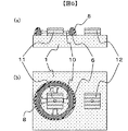
本発明の第二の実施形態について、図4を用いて説明する。図4(a)は、本実施例における光素子搭載部の詳細を示した平面図、図4(b)は、本実施例における光素子搭載部の詳細を示した断面図である。 A second embodiment of the present invention will be described with reference to FIG. FIG. 4A is a plan view showing details of the optical element mounting portion in this embodiment, and FIG. 4B is a cross-sectional view showing details of the optical element mounting portion in this embodiment.
本実施例は、実施例1の構成に対しさらに、発光素子11の発光波長λ1の光を反射する反射材8で光吸収樹脂6の上を覆っている。本実施例では、反射材8として熱硬化型の白色ペーストを用いている。反射材8は、光吸収樹脂6をUV硬化した後に、光吸収樹脂6の上にディスペンス法によって供給している。反射材8を供給後、熱硬化を実施することにより図4の構成は実現される。これにより、光吸収樹脂6で吸収しきれなかった漏れ光・は、反射材8で反射され、再度光吸収樹脂6で吸収される。したがって、漏れ光・の吸収効率が向上することとなり、光クロストークを低減させることができる。
In the present embodiment, the
本実施例では、反射材6として白色ペーストを用いたが、金属薄膜を用いてもかまわない。金属薄膜を蒸着により光吸収樹脂6上に形成することにより、白色ペーストと同様に光吸収樹脂6で吸収しきれなかった漏れ光10を反射させることができる。
In this embodiment, a white paste is used as the reflecting
また、反射材8として波長λ1における屈折率が、光吸収樹脂6のそれと異なる樹脂で代用してもかまわない。この場合、光吸収樹脂6と反射材8の界面で、光吸収樹脂6と反射材8の屈折率差に起因するフレネル反射が起こる。このフレネル反射による反射率Rは、波長λ1における光吸収樹脂6の屈折率をn3、反射材8の屈折率をn4、反射材8へ垂直入射すると仮定すると、R=(n4−n3)2/(n4+ n3)2×100(%)で表される。具体的には、n3 =1.2、n4 =1.5の場合、反射率R=(1.5−1.2)2/(1.5+1.2)2×100 ≒3.4 (%)となる。したがって、光吸収樹脂6で吸収しきれなかった光の3.4%が再度、光吸収樹脂6で吸収されることとなる。
Further, as the reflecting
本実施例においても、非接着層7の存在により光吸収樹脂6、反射材8ともに光素子搭載基板1と接着していない。そのため実施例1と同様に、温度変化時の光吸収樹脂6、反射材8の収縮により、発光素子11に歪みが発生することを抑制することができる。
Also in this embodiment, neither the light-absorbing
本発明の第三の実施形態について、図5を用いて説明する。 A third embodiment of the present invention will be described with reference to FIG.
図5(a)は、本実施例における光素子搭載部の詳細を示した平面図、図5(b)は、本実施例における光素子搭載部の詳細を示した断面図である。 FIG. 5A is a plan view showing details of the optical element mounting portion in the present embodiment, and FIG. 5B is a cross-sectional view showing details of the optical element mounting portion in the present embodiment.
本実施例では、図1のような構成の一芯双方向光送受信モジュールに対し、発光素子11の周囲を囲うように、発光素子11の発光波長λ1の光を吸収する光吸収樹脂6を配置している。その光素子搭載部の詳細を、図3を用いて説明する。
In the present embodiment, a light-absorbing
発光素子11の周囲には、発光素子11の発光波長λ1の光を吸収するUV硬化型樹脂を用いている。この光吸収樹脂6は、転写法により光素子搭載基板1上の発光素子11搭載部の周囲に塗布した後、UV照射により光吸収樹脂6を硬化させる。これにより、発光素子11はその周りを光吸収樹脂6の壁によって囲われることとなる。この構成により、発光素子11の側面から出射された漏れ光10は、光吸収樹脂6の壁に吸収されることとなる。そのため、発光素子11側面から直接または筐体3での散乱により、受光素子12へ入射する漏れ光10を低減することが可能となる。
A UV curable resin that absorbs light having a light emission wavelength λ 1 of the
本実施例では、光吸収樹脂6は発光素子1と接触しない構造となっている。そのため、実施例1のように、非接着層7が光素子搭載基板1に形成されていなくても、温度変化時の光吸収樹脂6の収縮が起きても発光素子1に歪みが発生しないこととなる。
In this embodiment, the
なお、本実施例では光吸収樹脂6として波長λ1の光を吸収するUV硬化型樹脂を用いたが、実施例1と同様に、これに囚われる必要はなく例えば、波長λ1の光を吸収する物質(粉末)とUV硬化型樹脂を混合させたものでもかまわない。また、黒色の封止用樹脂でもかまわない。
In the present embodiment, a UV curable resin that absorbs light of wavelength λ 1 is used as the
本発明の第四の実施形態について、図6を用いて説明する。図6(a)は、本実施例における光素子搭載部の詳細を示した平面図、図6(b)は、本実施例における光素子搭載部の詳細を示した断面図である。 A fourth embodiment of the present invention will be described with reference to FIG. 6A is a plan view showing details of the optical element mounting portion in the present embodiment, and FIG. 6B is a cross-sectional view showing details of the optical element mounting portion in the present embodiment.
本実施例は、実施例3の構成に対しさらに、光吸収樹脂6の壁の外周を覆うように、発光素子11の発光波長λ1の光を反射する反射材8を配置する。本実施例では、反射材8として熱硬化型の白色ペーストを用いている。反射材8は、光吸収樹脂6をUV硬化した後に、光吸収樹脂6の壁の外周を覆うように、ディスペンス法によって供給している。反射材8を供給後、熱硬化を実施することにより図6の構成は実現される。これにより、光吸収樹脂6の壁で吸収しきれなかった漏れ光10は、反射材8で反射され、再度光吸収樹脂6で吸収される。したがって、漏れ光10の吸収効率が向上することとなり、光クロストークを低減させることができる。
In the present embodiment, in addition to the configuration of the third embodiment, a
本実施例においても、光吸収樹脂6は発光素子1と接触しない構造となっている。そのため、実施例1のように、非接着層7が光素子搭載基板1に形成されていなくても、温度変化時の光吸収樹脂6の収縮が起きても発光素子1に歪みが発生しないこととなる。
Also in this embodiment, the
本実施例では、反射材8として白色ペーストを用いたが、実施例2と同様に、金属薄膜や波長λ1における屈折率が、光吸収樹脂6のそれと異なる樹脂で代用してもかまわない。
In the present embodiment, a white paste is used as the reflecting
本発明の第五の実施形態について、図7を用いて説明する。図7(a)は、本実施例における光素子搭載部の詳細を示した平面図、図7(b)は、本実施例における光素子搭載部の詳細を示した断面図である。 A fifth embodiment of the present invention will be described with reference to FIG. FIG. 7A is a plan view showing details of the optical element mounting portion in the present embodiment, and FIG. 7B is a cross-sectional view showing details of the optical element mounting portion in the present embodiment.
本実施例では、図1のような構成の一芯双方向光送受信モジュールにおいて、発光素子11として、その側面が発光素子11の発光波長λ1の光を吸収する光吸収する材質によりコーティングされたものを用いる。その光素子搭載部の詳細を、図3を用いて説明する。
In the present embodiment, in the single-core bidirectional optical transceiver module configured as shown in FIG. 1, the side surface of the
発光素子11の側面のコーティング層・の材質として、本実施例では発光素子11の発光波長λ1の光を吸収する光吸収する光吸収樹脂を用いている。このコーティング層9は、発光素子11を光素子搭載基板1に搭載する前に、光吸収樹脂を噴霧することにより予め形成されている。これにより、発光素子11側面からの漏れ光10は、コーティング層9により吸収されることとなる。そのため、発光素子11側面から直接または筐体3での散乱により、受光素子12へ入射する漏れ光・を低減することが可能となり光クロストークを抑制することができる。
As a material for the coating layer on the side surface of the
また、予め側面がコーティングされた発光素子11を光素子搭載基板に搭載しているため、コーティング層9と光素子搭載基板1は接着していない。そのため、温度変化があっても、本質的にコーティング層9の収縮による歪みが発光素子11に発生することのない構造となっている。
Further, since the
なお、本実施例ではコーティング層9の材質として光吸収樹脂を用いているが、発光波長λ1の光を吸収する光吸収する材質であればなんでもよく、望ましくは噴霧しやすい材質が好適である。
Although this embodiment uses the light-absorbent resin as the material of the
本発明は、発光素子と受光素子を具備する光モジュールを用いた情報通信装置を使用する分野、例えば光通信モジュール、光記録モジュール、高速スイッチング装置(ルータ、サーバなど)、などに利用可能である。 INDUSTRIAL APPLICABILITY The present invention can be used in a field where an information communication device using an optical module including a light emitting element and a light receiving element is used, for example, an optical communication module, an optical recording module, a high-speed switching device (router, server, etc.). .
1・・・光素子搭載基板、10・・・漏れ光、11・・・発光素子、12・・・受光素子、2・・・光合分波器、21・・・透明基板、22a、22b・・・波長選択フィルタ、
3・・・CANステム、31・・・光導波路コア、4・・・レンズ、5・・・光ファイバ、6・・・光吸収樹脂、7・・・非接着層、8・・・反射材、9・・・コーティング材。
DESCRIPTION OF
DESCRIPTION OF SYMBOLS 3 ... CAN stem, 31 ... Optical waveguide core, 4 ... Lens, 5 ... Optical fiber, 6 ... Light absorption resin, 7 ... Non-adhesion layer, 8 ... Reflective material , 9 ... Coating material.
Claims (12)
前記基板上に設けられ、上面に発光部を有する発光素子と、
前記基板上に設けられた受光素子とを備えた光モジュールにおいて、
前記発光素子の側面を覆うように、前記発光素子の発光波長の光を吸収する光吸収樹脂を配置し、
前記光吸収樹脂と前記基板の間には、前記光吸収樹脂と非接着の部材が配置されていることを特徴とする光モジュール。 A substrate,
A light emitting element provided on the substrate and having a light emitting portion on an upper surface;
In an optical module comprising a light receiving element provided on the substrate,
A light-absorbing resin that absorbs light of the emission wavelength of the light-emitting element is disposed so as to cover the side surface of the light-emitting element,
An optical module, wherein a member that is not bonded to the light absorbing resin is disposed between the light absorbing resin and the substrate.
前記光吸収樹脂の上を覆うように、前記発光素子の発光波長の光を反射する反射材が配置されていることを特徴とする光モジュール。 The optical module according to claim 1,
An optical module, wherein a reflective material that reflects light having a light emission wavelength of the light emitting element is disposed so as to cover the light absorbing resin.
前記反射材が樹脂であることを特徴とする光モジュール。 The optical module according to claim 2,
The optical module, wherein the reflective material is a resin.
前記基板上に設けられた発光素子と、
前記基板上に設けられた受光素子を備えた光モジュールにおいて、
前記発光素子の周囲を囲うように、前記発光素子の発光波長の光を吸収する光吸収樹脂が配置され、
前記光吸収樹脂と前記基板の間には、前記光吸収樹脂と非接着の部材が配置されていることを特徴とする光モジュール。 A substrate,
A light emitting device provided on the substrate;
In an optical module comprising a light receiving element provided on the substrate,
A light-absorbing resin that absorbs light of the emission wavelength of the light-emitting element is disposed so as to surround the light-emitting element ,
An optical module , wherein a member that is not bonded to the light absorbing resin is disposed between the light absorbing resin and the substrate .
前記光吸収樹脂の外周を覆うように、前記発光素子の発光波長の光を反射する反射材が配置されていることを特徴とする光モジュール。 The optical module according to claim 4,
An optical module, wherein a reflective material that reflects light having a light emission wavelength of the light emitting element is disposed so as to cover an outer periphery of the light absorbing resin.
前記反射材が樹脂であることを特徴とする光モジュール。 The optical module according to claim 5,
The optical module, wherein the reflective material is a resin.
前記光吸収樹脂が、透明樹脂と、前記発光素子の発光波長の光を吸収する光吸収材とを混合することにより構成されていることを特徴とする光モジュール。 The optical module according to any one of claims 1 to 6 ,
The optical module, wherein the light absorbing resin is configured by mixing a transparent resin and a light absorbing material that absorbs light having an emission wavelength of the light emitting element.
前記光吸収樹脂が、黒色の封止樹脂により構成されていることを特徴とする光モジュール。 The optical module according to any one of claims 1 to 7 ,
The optical module, wherein the light absorbing resin is made of a black sealing resin.
前記非接着な部材がテフロン(登録商標)であることを特徴とする光モジュール。 The optical module according to any one of claims 1 to 3,
An optical module, wherein the non-adhering member is Teflon (registered trademark).
前記反射材が白色ペーストにより構成されていることを特徴とする光モジュール。 The optical module according to claim 3 or 6,
An optical module, wherein the reflective material is made of a white paste.
前記反射材が、前記発光素子の発光波長における屈折率が、前記光吸収樹脂の前記発光素子の発光波長における屈折率と異なる樹脂により構成されていることを特徴とする光モジュール。 The optical module according to claim 3 or 6,
The optical module, wherein the reflective material is made of a resin having a refractive index at a light emission wavelength of the light emitting element that is different from a refractive index of the light absorbing resin at a light emission wavelength of the light emitting element.
請求項1乃至11のいずれかに記載の光モジュールと、
前記光ファイバからの光を前記光モジュールの受光素子に出射するとともに、前記光モジュールの発光素子からの光を前記光ファイバに出射するように合波及び分波を行う光合分波器と、
前記光モジュールと前記光合分波器を格納する筐体とを備えたことを特徴とする光送受信モジュール。 In an optical transceiver module connected to an optical fiber,
An optical module according to any one of claims 1 to 11 ,
An optical multiplexer / demultiplexer that multiplexes and demultiplexes the light from the optical fiber to the light receiving element of the optical module and emits the light from the light emitting element of the optical module to the optical fiber;
An optical transceiver module comprising the optical module and a housing for storing the optical multiplexer / demultiplexer.
Priority Applications (3)
| Application Number | Priority Date | Filing Date | Title |
|---|---|---|---|
| JP2008280697A JP4982469B2 (en) | 2008-10-31 | 2008-10-31 | Optical module |
| US13/126,898 US8449204B2 (en) | 2008-10-31 | 2009-06-11 | Optical module |
| PCT/JP2009/060691 WO2010050265A1 (en) | 2008-10-31 | 2009-06-11 | Optical module |
Applications Claiming Priority (1)
| Application Number | Priority Date | Filing Date | Title |
|---|---|---|---|
| JP2008280697A JP4982469B2 (en) | 2008-10-31 | 2008-10-31 | Optical module |
Publications (3)
| Publication Number | Publication Date |
|---|---|
| JP2010109204A JP2010109204A (en) | 2010-05-13 |
| JP2010109204A5 JP2010109204A5 (en) | 2011-04-14 |
| JP4982469B2 true JP4982469B2 (en) | 2012-07-25 |
Family
ID=42128635
Family Applications (1)
| Application Number | Title | Priority Date | Filing Date |
|---|---|---|---|
| JP2008280697A Expired - Fee Related JP4982469B2 (en) | 2008-10-31 | 2008-10-31 | Optical module |
Country Status (3)
| Country | Link |
|---|---|
| US (1) | US8449204B2 (en) |
| JP (1) | JP4982469B2 (en) |
| WO (1) | WO2010050265A1 (en) |
Families Citing this family (6)
| Publication number | Priority date | Publication date | Assignee | Title |
|---|---|---|---|---|
| KR101342097B1 (en) * | 2011-10-26 | 2013-12-18 | 한국전자통신연구원 | Multi-channel optical module |
| TW201436178A (en) * | 2013-02-13 | 2014-09-16 | 新力股份有限公司 | Light-emitting device |
| JP6166150B2 (en) * | 2013-10-29 | 2017-07-19 | アルプス電気株式会社 | Receiver |
| DE102017123798B4 (en) * | 2017-10-12 | 2022-03-03 | OSRAM Opto Semiconductors Gesellschaft mit beschränkter Haftung | Semiconductor lasers and manufacturing processes for optoelectronic semiconductor components |
| EP3800810A4 (en) * | 2018-08-27 | 2021-07-21 | Huawei Technologies Co., Ltd. | COMBINED LIGHT TRANSMITTER AND RECEPTION COMPONENTS, COMBINED OPTICAL MODULE, COMMUNICATION DEVICE AND PASSIVE OPTICAL NETWORK SYSTEM |
| CN113227861B (en) | 2018-12-26 | 2022-11-11 | 华为技术有限公司 | Multi-channel mode converter with silicon lens |
Family Cites Families (8)
| Publication number | Priority date | Publication date | Assignee | Title |
|---|---|---|---|---|
| JPH0273208A (en) | 1988-09-08 | 1990-03-13 | Nec Corp | Optical fiber packaging system |
| JP3792040B2 (en) | 1998-03-06 | 2006-06-28 | 松下電器産業株式会社 | Bidirectional optical semiconductor device |
| JP2000075155A (en) * | 1998-09-02 | 2000-03-14 | Nippon Telegr & Teleph Corp <Ntt> | Optical module |
| US7212556B1 (en) | 1999-02-17 | 2007-05-01 | Matsushita Electric Industrial Co., Ltd. | Semiconductor laser device optical disk apparatus and optical integrated unit |
| JP3456938B2 (en) * | 1999-02-17 | 2003-10-14 | 松下電器産業株式会社 | Semiconductor laser device, optical disk device, and optical integrated device |
| JP3766780B2 (en) * | 2000-05-12 | 2006-04-19 | シャープ株式会社 | Semiconductor laser device |
| JP2004138749A (en) | 2002-10-17 | 2004-05-13 | Matsushita Electric Ind Co Ltd | Optical transmitting / receiving module, mounting method thereof, and optical transmitting / receiving device |
| JP2008263047A (en) * | 2007-04-12 | 2008-10-30 | Shinko Electric Ind Co Ltd | Optical semiconductor element cap, optical semiconductor element package, and optical pickup device |
-
2008
- 2008-10-31 JP JP2008280697A patent/JP4982469B2/en not_active Expired - Fee Related
-
2009
- 2009-06-11 US US13/126,898 patent/US8449204B2/en not_active Expired - Fee Related
- 2009-06-11 WO PCT/JP2009/060691 patent/WO2010050265A1/en not_active Ceased
Also Published As
| Publication number | Publication date |
|---|---|
| US8449204B2 (en) | 2013-05-28 |
| US20110243512A1 (en) | 2011-10-06 |
| JP2010109204A (en) | 2010-05-13 |
| WO2010050265A1 (en) | 2010-05-06 |
Similar Documents
| Publication | Publication Date | Title |
|---|---|---|
| JP3861816B2 (en) | Optical transceiver module and manufacturing method thereof | |
| US9110256B2 (en) | Lens array and manufacturing method thereof | |
| JP4982469B2 (en) | Optical module | |
| US9488792B2 (en) | Optical receptacle, and optical module provided with same | |
| CN102667565A (en) | Lens array and optical module provided therewith | |
| JP5758658B2 (en) | Lens array and optical module having the same | |
| CN100359830C (en) | bidirectional optical transmission device | |
| JP2011133807A (en) | Lens array and optical module equipped with the lens array | |
| JPWO2008126836A1 (en) | Optical encoder | |
| JP6728639B2 (en) | Optical wiring connection structure and optical wiring connection method | |
| JP2011211152A (en) | Lens array and optical module with the same | |
| US9110257B2 (en) | Optical receptacle and optical module provided with same | |
| JP2009151106A (en) | Single fiber bidirectional optical device | |
| WO2020050166A1 (en) | Optical module | |
| JP6122380B2 (en) | Optical module | |
| JP2007187793A (en) | Optical module | |
| TW201323952A (en) | Optical coupling module and method of making the same | |
| JP3929968B2 (en) | Optical connector | |
| JP3936330B2 (en) | Optical connector and manufacturing method thereof | |
| CN108700720B (en) | Optical receptacle and optical module | |
| TWI573407B (en) | Optical communication module | |
| JP2020056894A (en) | Optical path conversion component, optical waveguide with optical path conversion component, optical module, and electronic apparatus | |
| JP7840751B2 (en) | Optical modules for encoders and reflective encoders | |
| JP2008020721A (en) | Parallel optical transmitter-receiver | |
| JP2010157666A (en) | Light emitting device |
Legal Events
| Date | Code | Title | Description |
|---|---|---|---|
| A521 | Written amendment |
Free format text: JAPANESE INTERMEDIATE CODE: A523 Effective date: 20110224 |
|
| A621 | Written request for application examination |
Free format text: JAPANESE INTERMEDIATE CODE: A621 Effective date: 20110224 |
|
| TRDD | Decision of grant or rejection written | ||
| A01 | Written decision to grant a patent or to grant a registration (utility model) |
Free format text: JAPANESE INTERMEDIATE CODE: A01 Effective date: 20120327 |
|
| A01 | Written decision to grant a patent or to grant a registration (utility model) |
Free format text: JAPANESE INTERMEDIATE CODE: A01 |
|
| A61 | First payment of annual fees (during grant procedure) |
Free format text: JAPANESE INTERMEDIATE CODE: A61 Effective date: 20120423 |
|
| FPAY | Renewal fee payment (event date is renewal date of database) |
Free format text: PAYMENT UNTIL: 20150427 Year of fee payment: 3 |
|
| LAPS | Cancellation because of no payment of annual fees |