JP4982469B2 - 光モジュール - Google Patents
光モジュール Download PDFInfo
- Publication number
- JP4982469B2 JP4982469B2 JP2008280697A JP2008280697A JP4982469B2 JP 4982469 B2 JP4982469 B2 JP 4982469B2 JP 2008280697 A JP2008280697 A JP 2008280697A JP 2008280697 A JP2008280697 A JP 2008280697A JP 4982469 B2 JP4982469 B2 JP 4982469B2
- Authority
- JP
- Japan
- Prior art keywords
- light
- optical module
- optical
- emitting element
- light emitting
- Prior art date
- Legal status (The legal status is an assumption and is not a legal conclusion. Google has not performed a legal analysis and makes no representation as to the accuracy of the status listed.)
- Expired - Fee Related
Links
Images



Classifications
-
- G—PHYSICS
- G02—OPTICS
- G02B—OPTICAL ELEMENTS, SYSTEMS OR APPARATUS
- G02B6/00—Light guides; Structural details of arrangements comprising light guides and other optical elements, e.g. couplings
- G02B6/24—Coupling light guides
- G02B6/42—Coupling light guides with opto-electronic elements
- G02B6/4201—Packages, e.g. shape, construction, internal or external details
- G02B6/4246—Bidirectionally operating package structures
-
- G—PHYSICS
- G02—OPTICS
- G02B—OPTICAL ELEMENTS, SYSTEMS OR APPARATUS
- G02B6/00—Light guides; Structural details of arrangements comprising light guides and other optical elements, e.g. couplings
- G02B6/24—Coupling light guides
- G02B6/26—Optical coupling means
- G02B6/28—Optical coupling means having data bus means, i.e. plural waveguides interconnected and providing an inherently bidirectional system by mixing and splitting signals
- G02B6/293—Optical coupling means having data bus means, i.e. plural waveguides interconnected and providing an inherently bidirectional system by mixing and splitting signals with wavelength selective means
- G02B6/29346—Optical coupling means having data bus means, i.e. plural waveguides interconnected and providing an inherently bidirectional system by mixing and splitting signals with wavelength selective means operating by wave or beam interference
- G02B6/29361—Interference filters, e.g. multilayer coatings, thin film filters, dichroic splitters or mirrors based on multilayers, WDM filters
- G02B6/29362—Serial cascade of filters or filtering operations, e.g. for a large number of channels
- G02B6/29365—Serial cascade of filters or filtering operations, e.g. for a large number of channels in a multireflection configuration, i.e. beam following a zigzag path between filters or filtering operations
- G02B6/29367—Zigzag path within a transparent optical block, e.g. filter deposited on an etalon, glass plate, wedge acting as a stable spacer
-
- H—ELECTRICITY
- H01—ELECTRIC ELEMENTS
- H01S—DEVICES USING THE PROCESS OF LIGHT AMPLIFICATION BY STIMULATED EMISSION OF RADIATION [LASER] TO AMPLIFY OR GENERATE LIGHT; DEVICES USING STIMULATED EMISSION OF ELECTROMAGNETIC RADIATION IN WAVE RANGES OTHER THAN OPTICAL
- H01S2301/00—Functional characteristics
- H01S2301/17—Semiconductor lasers comprising special layers
- H01S2301/176—Specific passivation layers on surfaces other than the emission facet
-
- H—ELECTRICITY
- H01—ELECTRIC ELEMENTS
- H01S—DEVICES USING THE PROCESS OF LIGHT AMPLIFICATION BY STIMULATED EMISSION OF RADIATION [LASER] TO AMPLIFY OR GENERATE LIGHT; DEVICES USING STIMULATED EMISSION OF ELECTROMAGNETIC RADIATION IN WAVE RANGES OTHER THAN OPTICAL
- H01S5/00—Semiconductor lasers
- H01S5/005—Optical components external to the laser cavity, specially adapted therefor, e.g. for homogenisation or merging of the beams or for manipulating laser pulses, e.g. pulse shaping
-
- H—ELECTRICITY
- H01—ELECTRIC ELEMENTS
- H01S—DEVICES USING THE PROCESS OF LIGHT AMPLIFICATION BY STIMULATED EMISSION OF RADIATION [LASER] TO AMPLIFY OR GENERATE LIGHT; DEVICES USING STIMULATED EMISSION OF ELECTROMAGNETIC RADIATION IN WAVE RANGES OTHER THAN OPTICAL
- H01S5/00—Semiconductor lasers
- H01S5/02—Structural details or components not essential to laser action
- H01S5/022—Mountings; Housings
- H01S5/02208—Mountings; Housings characterised by the shape of the housings
- H01S5/02212—Can-type, e.g. TO-CAN housings with emission along or parallel to symmetry axis
-
- H—ELECTRICITY
- H01—ELECTRIC ELEMENTS
- H01S—DEVICES USING THE PROCESS OF LIGHT AMPLIFICATION BY STIMULATED EMISSION OF RADIATION [LASER] TO AMPLIFY OR GENERATE LIGHT; DEVICES USING STIMULATED EMISSION OF ELECTROMAGNETIC RADIATION IN WAVE RANGES OTHER THAN OPTICAL
- H01S5/00—Semiconductor lasers
- H01S5/02—Structural details or components not essential to laser action
- H01S5/022—Mountings; Housings
- H01S5/02218—Material of the housings; Filling of the housings
- H01S5/02234—Resin-filled housings; the housings being made of resin
-
- H—ELECTRICITY
- H01—ELECTRIC ELEMENTS
- H01S—DEVICES USING THE PROCESS OF LIGHT AMPLIFICATION BY STIMULATED EMISSION OF RADIATION [LASER] TO AMPLIFY OR GENERATE LIGHT; DEVICES USING STIMULATED EMISSION OF ELECTROMAGNETIC RADIATION IN WAVE RANGES OTHER THAN OPTICAL
- H01S5/00—Semiconductor lasers
- H01S5/02—Structural details or components not essential to laser action
- H01S5/022—Mountings; Housings
- H01S5/0225—Out-coupling of light
- H01S5/02251—Out-coupling of light using optical fibres
-
- H—ELECTRICITY
- H01—ELECTRIC ELEMENTS
- H01S—DEVICES USING THE PROCESS OF LIGHT AMPLIFICATION BY STIMULATED EMISSION OF RADIATION [LASER] TO AMPLIFY OR GENERATE LIGHT; DEVICES USING STIMULATED EMISSION OF ELECTROMAGNETIC RADIATION IN WAVE RANGES OTHER THAN OPTICAL
- H01S5/00—Semiconductor lasers
- H01S5/02—Structural details or components not essential to laser action
- H01S5/022—Mountings; Housings
- H01S5/0225—Out-coupling of light
- H01S5/02257—Out-coupling of light using windows, e.g. specially adapted for back-reflecting light to a detector inside the housing
Landscapes
- Physics & Mathematics (AREA)
- General Physics & Mathematics (AREA)
- Optics & Photonics (AREA)
- Optical Couplings Of Light Guides (AREA)
- Semiconductor Lasers (AREA)
Description
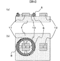
3・・・CANステム、31・・・光導波路コア、4・・・レンズ、5・・・光ファイバ、6・・・光吸収樹脂、7・・・非接着層、8・・・反射材、9・・・コーティング材。
Claims (12)
- 基板と、
前記基板上に設けられ、上面に発光部を有する発光素子と、
前記基板上に設けられた受光素子とを備えた光モジュールにおいて、
前記発光素子の側面を覆うように、前記発光素子の発光波長の光を吸収する光吸収樹脂を配置し、
前記光吸収樹脂と前記基板の間には、前記光吸収樹脂と非接着の部材が配置されていることを特徴とする光モジュール。 - 請求項1に記載の光モジュールにおいて、
前記光吸収樹脂の上を覆うように、前記発光素子の発光波長の光を反射する反射材が配置されていることを特徴とする光モジュール。 - 請求項2に記載の光モジュールにおいて、
前記反射材が樹脂であることを特徴とする光モジュール。 - 基板と、
前記基板上に設けられた発光素子と、
前記基板上に設けられた受光素子を備えた光モジュールにおいて、
前記発光素子の周囲を囲うように、前記発光素子の発光波長の光を吸収する光吸収樹脂が配置され、
前記光吸収樹脂と前記基板の間には、前記光吸収樹脂と非接着の部材が配置されていることを特徴とする光モジュール。 - 請求項4に記載の光モジュールにおいて、
前記光吸収樹脂の外周を覆うように、前記発光素子の発光波長の光を反射する反射材が配置されていることを特徴とする光モジュール。 - 請求項5に記載の光モジュールにおいて、
前記反射材が樹脂であることを特徴とする光モジュール。 - 請求項1から6のいずれかに記載の光モジュールにおいて、
前記光吸収樹脂が、透明樹脂と、前記発光素子の発光波長の光を吸収する光吸収材とを混合することにより構成されていることを特徴とする光モジュール。 - 請求項1から7のいずれかに記載の光モジュールにおいて、
前記光吸収樹脂が、黒色の封止樹脂により構成されていることを特徴とする光モジュール。 - 請求項1から3のいずれかに記載の光モジュールにおいて、
前記非接着な部材がテフロン(登録商標)であることを特徴とする光モジュール。 - 請求項3または請求項6に記載の光モジュールにおいて、
前記反射材が白色ペーストにより構成されていることを特徴とする光モジュール。 - 請求項3または請求項6に記載の光モジュールにおいて、
前記反射材が、前記発光素子の発光波長における屈折率が、前記光吸収樹脂の前記発光素子の発光波長における屈折率と異なる樹脂により構成されていることを特徴とする光モジュール。 - 光ファイバに接続される光送受信モジュールにおいて、
請求項1乃至11のいずれかに記載の光モジュールと、
前記光ファイバからの光を前記光モジュールの受光素子に出射するとともに、前記光モジュールの発光素子からの光を前記光ファイバに出射するように合波及び分波を行う光合分波器と、
前記光モジュールと前記光合分波器を格納する筐体とを備えたことを特徴とする光送受信モジュール。
Priority Applications (3)
| Application Number | Priority Date | Filing Date | Title |
|---|---|---|---|
| JP2008280697A JP4982469B2 (ja) | 2008-10-31 | 2008-10-31 | 光モジュール |
| US13/126,898 US8449204B2 (en) | 2008-10-31 | 2009-06-11 | Optical module |
| PCT/JP2009/060691 WO2010050265A1 (ja) | 2008-10-31 | 2009-06-11 | 光モジュール |
Applications Claiming Priority (1)
| Application Number | Priority Date | Filing Date | Title |
|---|---|---|---|
| JP2008280697A JP4982469B2 (ja) | 2008-10-31 | 2008-10-31 | 光モジュール |
Publications (3)
| Publication Number | Publication Date |
|---|---|
| JP2010109204A JP2010109204A (ja) | 2010-05-13 |
| JP2010109204A5 JP2010109204A5 (ja) | 2011-04-14 |
| JP4982469B2 true JP4982469B2 (ja) | 2012-07-25 |
Family
ID=42128635
Family Applications (1)
| Application Number | Title | Priority Date | Filing Date |
|---|---|---|---|
| JP2008280697A Expired - Fee Related JP4982469B2 (ja) | 2008-10-31 | 2008-10-31 | 光モジュール |
Country Status (3)
| Country | Link |
|---|---|
| US (1) | US8449204B2 (ja) |
| JP (1) | JP4982469B2 (ja) |
| WO (1) | WO2010050265A1 (ja) |
Families Citing this family (6)
| Publication number | Priority date | Publication date | Assignee | Title |
|---|---|---|---|---|
| KR101342097B1 (ko) * | 2011-10-26 | 2013-12-18 | 한국전자통신연구원 | 다채널 광모듈 |
| TW201436178A (zh) * | 2013-02-13 | 2014-09-16 | 新力股份有限公司 | 受光發光裝置 |
| JP6166150B2 (ja) * | 2013-10-29 | 2017-07-19 | アルプス電気株式会社 | 受光装置 |
| DE102017123798B4 (de) * | 2017-10-12 | 2022-03-03 | OSRAM Opto Semiconductors Gesellschaft mit beschränkter Haftung | Halbleiterlaser und Herstellungsverfahren für optoelektronische Halbleiterbauteile |
| EP3800810A4 (en) * | 2018-08-27 | 2021-07-21 | Huawei Technologies Co., Ltd. | COMPONENTS FOR LIGHT RECEPTION AND COMBINED TRANSMISSION RECEIVING, COMBINED OPTICAL MODULE, COMMUNICATION DEVICE AND PON SYSTEM |
| CN113227861B (zh) | 2018-12-26 | 2022-11-11 | 华为技术有限公司 | 具有硅透镜的多通道模式转换器 |
Family Cites Families (8)
| Publication number | Priority date | Publication date | Assignee | Title |
|---|---|---|---|---|
| JPH0273208A (ja) | 1988-09-08 | 1990-03-13 | Nec Corp | 光ファイバー実装方式 |
| JP3792040B2 (ja) | 1998-03-06 | 2006-06-28 | 松下電器産業株式会社 | 双方向光半導体装置 |
| JP2000075155A (ja) * | 1998-09-02 | 2000-03-14 | Nippon Telegr & Teleph Corp <Ntt> | 光モジュール |
| US7212556B1 (en) | 1999-02-17 | 2007-05-01 | Matsushita Electric Industrial Co., Ltd. | Semiconductor laser device optical disk apparatus and optical integrated unit |
| JP3456938B2 (ja) * | 1999-02-17 | 2003-10-14 | 松下電器産業株式会社 | 半導体レーザ装置、光ディスク装置及び光集積化装置 |
| JP3766780B2 (ja) * | 2000-05-12 | 2006-04-19 | シャープ株式会社 | 半導体レーザ装置 |
| JP2004138749A (ja) | 2002-10-17 | 2004-05-13 | Matsushita Electric Ind Co Ltd | 光送受信モジュール及びその実装方法並びに光送受信装置 |
| JP2008263047A (ja) * | 2007-04-12 | 2008-10-30 | Shinko Electric Ind Co Ltd | 光半導体素子用キャップ、光半導体素子用パッケージ及び光ピックアップ装置 |
-
2008
- 2008-10-31 JP JP2008280697A patent/JP4982469B2/ja not_active Expired - Fee Related
-
2009
- 2009-06-11 US US13/126,898 patent/US8449204B2/en not_active Expired - Fee Related
- 2009-06-11 WO PCT/JP2009/060691 patent/WO2010050265A1/ja not_active Ceased
Also Published As
| Publication number | Publication date |
|---|---|
| US8449204B2 (en) | 2013-05-28 |
| US20110243512A1 (en) | 2011-10-06 |
| JP2010109204A (ja) | 2010-05-13 |
| WO2010050265A1 (ja) | 2010-05-06 |
Similar Documents
| Publication | Publication Date | Title |
|---|---|---|
| JP3861816B2 (ja) | 光送受信モジュール及びその製造方法 | |
| US9110256B2 (en) | Lens array and manufacturing method thereof | |
| JP4982469B2 (ja) | 光モジュール | |
| US9488792B2 (en) | Optical receptacle, and optical module provided with same | |
| CN102667565A (zh) | 透镜阵列以及具备该透镜阵列的光学模块 | |
| JP5758658B2 (ja) | レンズアレイおよびこれを備えた光モジュール | |
| CN100359830C (zh) | 双向光传输装置 | |
| JP2011133807A (ja) | レンズアレイおよびこれを備えた光モジュール | |
| JPWO2008126836A1 (ja) | 光学式エンコーダ | |
| JP6728639B2 (ja) | 光配線接続構造、及び光配線接続方法 | |
| JP2011211152A (ja) | レンズアレイおよびこれを備えた光モジュール | |
| US9110257B2 (en) | Optical receptacle and optical module provided with same | |
| JP2009151106A (ja) | 一芯双方向光デバイス | |
| WO2020050166A1 (ja) | 光モジュール | |
| JP6122380B2 (ja) | 光モジュール | |
| JP2007187793A (ja) | 光モジュール | |
| TW201323952A (zh) | 光耦合模組及其製作方法 | |
| JP3929968B2 (ja) | 光コネクタ | |
| JP3936330B2 (ja) | 光コネクタおよびその製造方法 | |
| CN108700720B (zh) | 光插座及光模块 | |
| TWI573407B (zh) | 光通訊模組 | |
| JP2020056894A (ja) | 光路変換部品、光路変換部品付き光導波路、光モジュールおよび電子機器 | |
| JP7840751B2 (ja) | エンコーダ用光モジュール及び反射型エンコーダ | |
| JP2008020721A (ja) | 並列光送受信装置 | |
| JP2010157666A (ja) | 発光装置 |
Legal Events
| Date | Code | Title | Description |
|---|---|---|---|
| A521 | Written amendment |
Free format text: JAPANESE INTERMEDIATE CODE: A523 Effective date: 20110224 |
|
| A621 | Written request for application examination |
Free format text: JAPANESE INTERMEDIATE CODE: A621 Effective date: 20110224 |
|
| TRDD | Decision of grant or rejection written | ||
| A01 | Written decision to grant a patent or to grant a registration (utility model) |
Free format text: JAPANESE INTERMEDIATE CODE: A01 Effective date: 20120327 |
|
| A01 | Written decision to grant a patent or to grant a registration (utility model) |
Free format text: JAPANESE INTERMEDIATE CODE: A01 |
|
| A61 | First payment of annual fees (during grant procedure) |
Free format text: JAPANESE INTERMEDIATE CODE: A61 Effective date: 20120423 |
|
| FPAY | Renewal fee payment (event date is renewal date of database) |
Free format text: PAYMENT UNTIL: 20150427 Year of fee payment: 3 |
|
| LAPS | Cancellation because of no payment of annual fees |