JP4986785B2 - プローブカード - Google Patents
プローブカード Download PDFInfo
- Publication number
- JP4986785B2 JP4986785B2 JP2007244813A JP2007244813A JP4986785B2 JP 4986785 B2 JP4986785 B2 JP 4986785B2 JP 2007244813 A JP2007244813 A JP 2007244813A JP 2007244813 A JP2007244813 A JP 2007244813A JP 4986785 B2 JP4986785 B2 JP 4986785B2
- Authority
- JP
- Japan
- Prior art keywords
- probe
- contact
- layer
- substrate
- conductive layer
- Prior art date
- Legal status (The legal status is an assumption and is not a legal conclusion. Google has not performed a legal analysis and makes no representation as to the accuracy of the status listed.)
- Expired - Fee Related
Links
- 239000000523 sample Substances 0.000 title claims description 218
- 238000007689 inspection Methods 0.000 claims description 18
- 238000010030 laminating Methods 0.000 claims description 6
- 239000000758 substrate Substances 0.000 description 80
- XUIMIQQOPSSXEZ-UHFFFAOYSA-N Silicon Chemical compound [Si] XUIMIQQOPSSXEZ-UHFFFAOYSA-N 0.000 description 16
- 229910052710 silicon Inorganic materials 0.000 description 16
- 239000010703 silicon Substances 0.000 description 16
- 238000002844 melting Methods 0.000 description 11
- 230000008018 melting Effects 0.000 description 11
- 238000000034 method Methods 0.000 description 8
- 238000009713 electroplating Methods 0.000 description 7
- 238000007747 plating Methods 0.000 description 7
- 229910000679 solder Inorganic materials 0.000 description 5
- 230000015572 biosynthetic process Effects 0.000 description 4
- 239000004020 conductor Substances 0.000 description 4
- 238000004519 manufacturing process Methods 0.000 description 4
- 238000000059 patterning Methods 0.000 description 4
- 229920002120 photoresistant polymer Polymers 0.000 description 4
- 238000012360 testing method Methods 0.000 description 4
- 239000004065 semiconductor Substances 0.000 description 3
- 238000010586 diagram Methods 0.000 description 2
- 238000005530 etching Methods 0.000 description 2
- 238000010438 heat treatment Methods 0.000 description 2
- 230000002093 peripheral effect Effects 0.000 description 2
- 239000004593 Epoxy Substances 0.000 description 1
- 230000002349 favourable effect Effects 0.000 description 1
- 239000011521 glass Substances 0.000 description 1
- 239000000463 material Substances 0.000 description 1
- 239000011368 organic material Substances 0.000 description 1
Images




Landscapes
- Measuring Leads Or Probes (AREA)
- Testing Or Measuring Of Semiconductors Or The Like (AREA)
Description
<プローブカード>
図1(a)及び(b)は、本発明の実施の形態1によるプローブカード10の一例を示した図であり、図中の(a)は、検査対象物側から見た平面図であり、図中の(b)は、側面図である。プローブカード10は、ガラスエポキシなどにより形成されたプローブ基板12と、プローブ基板12上に固着された複数のコンタクトプローブ11により構成される。
図2は、図1のプローブカード10の要部の一構成例を示した図であり、プローブ基板12上に形成されるコンタクトプローブ11が示されている。コンタクトプローブ11は、3つの導電層21〜23を積層することにより形成され、各導電層21〜23の端面21a〜23aにより形成された接合部1と、検査対象物上の電極パッドに接触させるための接触部4が先端部に形成されたビーム部2とを有している。
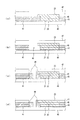
図4〜図6は、図2のコンタクトプローブ11の接合部1を形成する工程を模式的に示した断面図である。図4(a)には、犠牲層41が形成されたコンタクトプローブ形成用のシリコン基板40が示されている。コンタクトプローブ11の接合部1を形成する際には、まず、コンタクトプローブ形成用のシリコン基板40上に、導電層21〜23とは異なる導電性材料からなる犠牲層41が形成される。
実施の形態1では、外側の導電層21の端面21aを他の導電層22,23の端面よりも突出させて接合部1が形成される場合の例について説明した。これに対して、本実施の形態では、接触部4を形成する導電層の端面を他の導電層の端面よりも突出させる場合について説明する。
2 ビーム部
3a 端面
4 接触部
10 プローブカード
11 コンタクトプローブ
12 プローブ基板
13 外部端子
20 低融点層
21〜23 導電層
21a〜23a 端面
31 電極パッド
51 コンタクトプローブ
Claims (3)
- プローブ基板と、平板状で端面を上記プローブ基板上に突き合わせて接合される複数のコンタクトプローブとを備えたプローブカードにおいて、
上記複数のコンタクトプローブが、導電層を複数積層して構成され、上記端面が凹凸であって、上記端面において突出している層の位置がそれぞれ同一であることを特徴とするプローブカード。 - 上記コンタクトプローブは、検査対象物に向けて、一部の上記導電層を他の導電層よりも突出させることにより形成された接触部を有し、
上記接触部を形成する上記導電層が、上記端面内で最も突出している層を形成していることを特徴とする請求項1に記載のプローブカード。 - 上記コンタクトプローブは、3つの導電層を積層することにより形成され、中央の層が上記端面内で最も突出している層を形成していることを特徴とする請求項1又は2に記載のプローブカード。
Priority Applications (1)
| Application Number | Priority Date | Filing Date | Title |
|---|---|---|---|
| JP2007244813A JP4986785B2 (ja) | 2007-09-21 | 2007-09-21 | プローブカード |
Applications Claiming Priority (1)
| Application Number | Priority Date | Filing Date | Title |
|---|---|---|---|
| JP2007244813A JP4986785B2 (ja) | 2007-09-21 | 2007-09-21 | プローブカード |
Publications (2)
| Publication Number | Publication Date |
|---|---|
| JP2009074958A JP2009074958A (ja) | 2009-04-09 |
| JP4986785B2 true JP4986785B2 (ja) | 2012-07-25 |
Family
ID=40610065
Family Applications (1)
| Application Number | Title | Priority Date | Filing Date |
|---|---|---|---|
| JP2007244813A Expired - Fee Related JP4986785B2 (ja) | 2007-09-21 | 2007-09-21 | プローブカード |
Country Status (1)
| Country | Link |
|---|---|
| JP (1) | JP4986785B2 (ja) |
Families Citing this family (1)
| Publication number | Priority date | Publication date | Assignee | Title |
|---|---|---|---|---|
| TWI454710B (zh) * | 2012-09-19 | 2014-10-01 | Mpi Corp | Probe card and its manufacturing method |
Family Cites Families (4)
| Publication number | Priority date | Publication date | Assignee | Title |
|---|---|---|---|---|
| JPH0636209Y2 (ja) * | 1989-12-28 | 1994-09-21 | 小松ウオール工業株式会社 | 移動間仕切りの安全装置 |
| JP4014040B2 (ja) * | 2002-10-29 | 2007-11-28 | 日本電子材料株式会社 | プローブ |
| WO2007086147A1 (ja) * | 2006-01-25 | 2007-08-02 | Kabushiki Kaisha Nihon Micronics | 通電試験用プローブ、プローブ組立体およびその製造方法 |
| JP2007240235A (ja) * | 2006-03-07 | 2007-09-20 | Micronics Japan Co Ltd | 通電試験用プローブおよびプローブ組立体 |
-
2007
- 2007-09-21 JP JP2007244813A patent/JP4986785B2/ja not_active Expired - Fee Related
Also Published As
| Publication number | Publication date |
|---|---|
| JP2009074958A (ja) | 2009-04-09 |
Similar Documents
| Publication | Publication Date | Title |
|---|---|---|
| TWI517326B (zh) | 具有引線之基板 | |
| TW201030872A (en) | Probe card and manufacturing method thereof | |
| JP2012099352A (ja) | 接続端子構造及びその製造方法、並びにソケット | |
| JP2020165774A (ja) | 多ピン構造プローブ体及びプローブカード | |
| CN100592487C (zh) | 结合探针的方法以及使用该方法制造探针卡的方法 | |
| TWI482255B (zh) | 藉由嵌入跡線界定之導電墊 | |
| CN100490107C (zh) | 立式电接触元件的制造方法和立式电接触元件 | |
| KR101120405B1 (ko) | 프로브 블록 조립체 | |
| JP7471778B2 (ja) | プローブカード | |
| TWI434044B (zh) | 探針卡及其製作方法 | |
| JP4986785B2 (ja) | プローブカード | |
| JP2008536109A (ja) | プローブカード及びその製造方法 | |
| JP2005061851A (ja) | プローブカード用基板 | |
| JP6092729B2 (ja) | プローブカード及びその製造方法 | |
| JP2011075532A (ja) | プローブカード及びその製造方法 | |
| JP5462732B2 (ja) | シート状コネクタ、及びその製造方法 | |
| CN110007117A (zh) | 探针卡 | |
| CN101310375A (zh) | 探针板以及制造该探针板的方法 | |
| JP5700761B2 (ja) | 電気的接続装置 | |
| JP7700495B2 (ja) | 半導体装置 | |
| KR101024098B1 (ko) | 프로브 본딩 방법 | |
| KR100821674B1 (ko) | 프로브 어셈블리 | |
| JP5463517B2 (ja) | プローブ | |
| TWI678537B (zh) | 探針卡 | |
| WO2022208708A1 (ja) | プローブカード |
Legal Events
| Date | Code | Title | Description |
|---|---|---|---|
| A621 | Written request for application examination |
Free format text: JAPANESE INTERMEDIATE CODE: A621 Effective date: 20100805 |
|
| A977 | Report on retrieval |
Free format text: JAPANESE INTERMEDIATE CODE: A971007 Effective date: 20120411 |
|
| TRDD | Decision of grant or rejection written | ||
| A01 | Written decision to grant a patent or to grant a registration (utility model) |
Free format text: JAPANESE INTERMEDIATE CODE: A01 Effective date: 20120424 |
|
| A01 | Written decision to grant a patent or to grant a registration (utility model) |
Free format text: JAPANESE INTERMEDIATE CODE: A01 |
|
| A61 | First payment of annual fees (during grant procedure) |
Free format text: JAPANESE INTERMEDIATE CODE: A61 Effective date: 20120424 |
|
| R150 | Certificate of patent or registration of utility model |
Ref document number: 4986785 Country of ref document: JP Free format text: JAPANESE INTERMEDIATE CODE: R150 Free format text: JAPANESE INTERMEDIATE CODE: R150 |
|
| FPAY | Renewal fee payment (event date is renewal date of database) |
Free format text: PAYMENT UNTIL: 20150511 Year of fee payment: 3 |
|
| R250 | Receipt of annual fees |
Free format text: JAPANESE INTERMEDIATE CODE: R250 |
|
| R250 | Receipt of annual fees |
Free format text: JAPANESE INTERMEDIATE CODE: R250 |
|
| R250 | Receipt of annual fees |
Free format text: JAPANESE INTERMEDIATE CODE: R250 |
|
| R250 | Receipt of annual fees |
Free format text: JAPANESE INTERMEDIATE CODE: R250 |
|
| R250 | Receipt of annual fees |
Free format text: JAPANESE INTERMEDIATE CODE: R250 |
|
| R250 | Receipt of annual fees |
Free format text: JAPANESE INTERMEDIATE CODE: R250 |
|
| LAPS | Cancellation because of no payment of annual fees |