JP4986942B2 - リソグラフィシステム - Google Patents
リソグラフィシステム Download PDFInfo
- Publication number
- JP4986942B2 JP4986942B2 JP2008179652A JP2008179652A JP4986942B2 JP 4986942 B2 JP4986942 B2 JP 4986942B2 JP 2008179652 A JP2008179652 A JP 2008179652A JP 2008179652 A JP2008179652 A JP 2008179652A JP 4986942 B2 JP4986942 B2 JP 4986942B2
- Authority
- JP
- Japan
- Prior art keywords
- chuck
- thermal expansion
- encoder
- lithography
- movement
- Prior art date
- Legal status (The legal status is an assumption and is not a legal conclusion. Google has not performed a legal analysis and makes no representation as to the accuracy of the status listed.)
- Expired - Fee Related
Links
Images


Classifications
-
- H—ELECTRICITY
- H10—SEMICONDUCTOR DEVICES; ELECTRIC SOLID-STATE DEVICES NOT OTHERWISE PROVIDED FOR
- H10P—GENERIC PROCESSES OR APPARATUS FOR THE MANUFACTURE OR TREATMENT OF DEVICES COVERED BY CLASS H10
- H10P72/00—Handling or holding of wafers, substrates or devices during manufacture or treatment thereof
- H10P72/06—Apparatus for monitoring, sorting, marking, testing or measuring
- H10P72/0606—Position monitoring, e.g. misposition detection or presence detection
- H10P72/0608—Position monitoring, e.g. misposition detection or presence detection of substrates stored in a container, a magazine, a carrier, a boat or the like
-
- H—ELECTRICITY
- H10—SEMICONDUCTOR DEVICES; ELECTRIC SOLID-STATE DEVICES NOT OTHERWISE PROVIDED FOR
- H10P—GENERIC PROCESSES OR APPARATUS FOR THE MANUFACTURE OR TREATMENT OF DEVICES COVERED BY CLASS H10
- H10P72/00—Handling or holding of wafers, substrates or devices during manufacture or treatment thereof
- H10P72/50—Handling or holding of wafers, substrates or devices during manufacture or treatment thereof for positioning, orientation or alignment
- H10P72/57—Mask-wafer alignment
Landscapes
- Exposure And Positioning Against Photoresist Photosensitive Materials (AREA)
- Exposure Of Semiconductors, Excluding Electron Or Ion Beam Exposure (AREA)
- Container, Conveyance, Adherence, Positioning, Of Wafer (AREA)
- Length Measuring Devices By Optical Means (AREA)
Description
本発明は、対象物をリソグラフィツールに正確に位置決めするための装置及び方法に関する。レチクル又はウェハ等の位置決めされるべき対象物は、ある物理的特性を有するチャックによって拘束される。次いで、チャックはリソグラフィツール内に正確に位置決めされる。リソグラフィツールが作動すると、制御システムは、チャックの位置及び寸法を監視し、チャックによって保持された対象物がリソグラフィツール内に正確に位置決めされるように所要の調整を行う。
最初に、本発明が使用される環境を説明することが役立つ。図1は、本発明によるチャック110が配置される環境例を示している。装置100は、スキャニングリソグラフィツールに存在するような慣用の投影光学系である。レチクルステージ101に続いて、第1のレンズグループ120と、折り返しミラー130と、第2のレンズグループ140と、ビームスプリッタ150と、波長板160と、凹面鏡170と、第3のレンズグループ180と、ウェハステージ191とが配置されている。チャック110は通常、例えばレチクル112をレチクルステージ101に保持するために又はウェハ114をウェハステージ191に保持するために使用される。チャックは、リソグラフィツール内にミラー等の他の対象物を保持及び位置決めするために使用されてもよい。さらに、本発明によるチャックは、接触式リソグラフィツール等の、投影光学系を含まないリソグラフィツール又は、この例とは実質的に異なる投影光学系の設計を有するリソグラフィツールにおいて使用されてよい。
前記のように、チャック110は、慣用のチャックと比較した場合、高い比剛性及び高い熱伝導率を有する材料から製造されている。熱効果を測定するための装置と組み合わされた場合、これらの特性は、増大した制御帯域幅及び減じられた電力消費等の利点をフォトリソグラフィツールに提供する。表1は、慣用のチャック材料と、本発明のチャック材料との複数のよく知られた材料の有用な比較を提供している。

図2は、本発明のチャック110における熱補償を測定するための典型的な装置を示している。この装置は、上に記載された物理的特性を有するチャック110の熱膨張又は収縮を測定するためにエンコーダ220,220′を使用する。
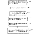
図3は、リソグラフィツールの制御システムの帯域幅又は作動周波数を増大する方法を示している。ステップ305において、上に説明したように、高い比剛性及び高い熱伝導率を有するチャックが提供される。これらの物理的特性はリソグラフィツールに利点を提供する。上に説明したように、高い比剛性はリソグラフィツールの制御システムにおける増大した帯域幅を許容するのに対し、高い熱伝導率はチャックにおける熱効果の正確な測定を許容する。
本発明の様々な実施形態が上に説明されたが、これらの実施形態は例として示されているだけであり、限定するものではないことが理解されるべきである。添付の請求項に定義されているような発明の思想及び範囲から逸脱することなく、これらの実施形態の形式及び詳細に様々な変更が加えられてよいことは当業者によって理解されるであろう。したがって、本発明の広さ及び範囲は、上述の典型的な実施形態の何れによっても制限されるべきではなく、添付の請求項及びそれらの請求項の均等物に基づいてのみ定義されるべきである。
Claims (14)
- 制御システムを有するリソグラフィシステムにおいて、
ステージと、
該ステージによって支持されておりかつ、高い比剛性及び高い熱伝導率を有するチャックであって、前記比剛性が約90M(m/s) 2 より高く、前記熱伝導率が、約25W/mKより高く、この場合Wはワット、mはメートル、Kはケルビン温度である、チャックと、
該チャックの熱膨張を少なくとも1つの次元で、該チャック上の互いに反対の縁部にそれぞれ配置された少なくとも2つの位置の変位を比較することにより測定するための手段と、
前記熱膨張に基づき前記チャックの熱ひずみを計算するとともに、該熱ひずみに基づいて別の次元における熱膨張を計算する手段と、
が設けられており、
前記チャックが工作物又は光学素子を支持しており、これにより前記チャックを移動させることにより前記工作物又は前記光学素子も移動するようになっており、
前記熱膨張に基づいて前記チャックの位置を調整する制御システムと、を備えるリソグラフィシステム。 - 前記チャックが、リソグラフィツールの投影光学系部分から実質的に隔離されている、請求項1記載のリソグラフィシステム。
- 前記チャックが磁気的に安定及び位置決めされている、請求項1又は請求項2記載のリソグラフィシステム。
- 前記比剛性が約90M〜150M(m/s)2である、請求項1乃至請求項3のいずれか一項記載のリソグラフィシステム。
- 前記熱伝導率が、約25〜250W/mKであり、この場合、Wはワット、mはメートル、Kはケルビン温度である、請求項1乃至請求項4のいずれか一項記載のリソグラフィシステム。
- 前記チャックが炭化ケイ素及びその複合物、窒化ケイ素及びその複合物又は窒化アルミニウム及びその複合物から形成されている、請求項1乃至請求項5のいずれか一項記載のリソグラフィシステム。
- 前記熱膨張を測定するための手段がエンコーダを含んでいる、請求項1乃至請求項6のいずれか一項記載のリソグラフィシステム。
- 前記エンコーダが:
前記チャックの第1の縁部及び第2の縁部に沿って位置決めされた線形のトラックの第1の対を有しており、該トラックの第1の対が、リソグラフィツールの定置のフレームに位置決めされたエンコーダヘッドの第1の対に対応しており、前記トラックの第1の対とヘッドの第1の対とが、第1の方向での前記チャックの相対移動の少なくとも2つの独立した測定を生ぜしめるために使用され;
前記チャックの第1の縁部及び第2の縁部に沿って位置決めされた線形のトラックの第2の対を有しており、該トラックの第2の対が、前記定置のフレームに位置決めされたエンコーダヘッドの第2の対に対応しており、前記トラックの第2の対とヘッドの第2の対とが、第1の方向に対して垂直な第2の方向での前記チャックの相対移動の少なくとも2つの独立した測定を生ぜしめるために使用され;
前記チャックの相対移動の前記独立した測定を比較するための手段を有している、請求項7記載のリソグラフィシステム。 - 前記エンコーダが:
前記チャックの第1の縁部に位置決めされた第1の線形のエンコーダトラックと、リソグラフィツールの定置のフレームに位置決めされた対応する第1のエンコーダヘッドとを有しており、これにより、前記第1の縁部に対して垂直な方向での前記フレームに対する前記第1のトラックの移動を測定するようになっており;
前記チャックの第2の縁部に位置決めされた第2の線形のエンコーダトラックを有しており、前記第2の縁部が前記第1の縁部に対して平行でかつ該第1の縁部に向き合っており、前記フレームに位置決めされた対応する第2のエンコーダヘッドを有しており、これにより、前記方向での前記フレームに対する前記第2のトラックの移動を測定するようになっており;
前記第1のトラックに対する前記第2のトラックの移動から前記方向での熱膨張が決定される、請求項7記載のリソグラフィシステム。 - 前記エンコーダが:
前記チャックに位置決めされた、第1の端部及び第2の端部を有する線形のエンコーダトラックを有しており;
該エンコーダトラックの前記第1の端部の近傍に、リソグラフィツールの定置のフレームに位置決めされた第1のエンコーダヘッドを有しており、これにより、前記トラックの長さに対して平行な方向での前記フレームに対する前記第1の端部の移動を測定するようになっており;
前記エンコーダトラックの前記第2の端部の近傍に、前記フレームに位置決めされた第2のエンコーダヘッドを有しており、これにより、前記方向での前記フレームに対する前記第2の端部の移動を測定するようになっており;
前記第1の端部に対するエンコーダトラックの前記第2の端部の前記移動から、前記方向での熱膨張が決定されるようになっている、請求項7記載のリソグラフィシステム。 - 熱膨張を測定するための前記手段が干渉計を含む、請求項1乃至請求項6のいずれか一項記載のリソグラフィシステム。
- 熱膨張を測定するための前記手段が:
リソグラフィツールの定置のフレームに位置決めされた干渉計からの第1の光ビームを反射するための、前記チャックに位置決めされた第1の平坦なミラーを有しており;
前記干渉計からの第2の光ビームを反射するための、前記チャックに位置決めされた、前記第1の平坦なミラーに対して平行でありかつ該第1の平坦なミラーに対して同一平面に位置していない第2の平坦なミラーを有しており;
干渉計によって測定された前記第1のミラーに対する前記第2のミラーの移動から、前記ミラーに対して垂直な方向での熱膨張が決定されるようになっている、請求項11記載のリソグラフィシステム。 - 熱膨張を測定するための前記手段が:
リソグラフィツールの定置のフレームに位置決めされた干渉計からの第1の光ビームを反射するための、前記チャックの第1の角の近傍に位置決めされた第1の逆反射装置と;
前記干渉計からの第1の光ビームに対して平行な第2のビームを反射するための、前記チャックの第2の角の近傍に位置決めされた第2の逆反射装置とを有しており;
前記干渉計によって測定された前記第1の逆反射装置に対する前記第2の逆反射装置の移動から、前記ビームに対して平行な方向での熱膨張が決定されるようになっている、請求項11記載のリソグラフィシステム。 - 熱膨張を測定するための前記手段が:
前記チャックの第1の側に沿って位置決めされた第1の平坦なストリップと、第1のセンサヘッドとを有しており、該第1のセンサヘッドが、該第1のセンサヘッドと前記第1のストリップとの間の距離を測定するためにリソグラフィツールの定置のフレームに位置決めされており;
前記第1の側に対して平行でかつ該第1の側に向き合った、前記チャックの第2の側に沿って位置決めされた第2の平坦なストリップと、第2のセンサヘッドとを有しており、該第2のセンサヘッドが、該第2のセンサヘッドと前記第2のストリップとの間の距離を測定するために前記フレームに位置決めされており;
前記第1のストリップに対する前記第2のストリップの移動から、前記ストリップに対して垂直な方向での熱膨張が決定されるようになっている、請求項1乃至請求項6のいずれか一項記載のリソグラフィシステム。
Applications Claiming Priority (2)
| Application Number | Priority Date | Filing Date | Title |
|---|---|---|---|
| US10/448027 | 2003-05-30 | ||
| US10/448,027 US7025498B2 (en) | 2003-05-30 | 2003-05-30 | System and method of measuring thermal expansion |
Related Parent Applications (1)
| Application Number | Title | Priority Date | Filing Date |
|---|---|---|---|
| JP2004162319A Division JP4610231B2 (ja) | 2003-05-30 | 2004-05-31 | 熱膨張補償を備えるステージ |
Publications (2)
| Publication Number | Publication Date |
|---|---|
| JP2009010393A JP2009010393A (ja) | 2009-01-15 |
| JP4986942B2 true JP4986942B2 (ja) | 2012-07-25 |
Family
ID=33451401
Family Applications (2)
| Application Number | Title | Priority Date | Filing Date |
|---|---|---|---|
| JP2004162319A Expired - Fee Related JP4610231B2 (ja) | 2003-05-30 | 2004-05-31 | 熱膨張補償を備えるステージ |
| JP2008179652A Expired - Fee Related JP4986942B2 (ja) | 2003-05-30 | 2008-07-10 | リソグラフィシステム |
Family Applications Before (1)
| Application Number | Title | Priority Date | Filing Date |
|---|---|---|---|
| JP2004162319A Expired - Fee Related JP4610231B2 (ja) | 2003-05-30 | 2004-05-31 | 熱膨張補償を備えるステージ |
Country Status (2)
| Country | Link |
|---|---|
| US (1) | US7025498B2 (ja) |
| JP (2) | JP4610231B2 (ja) |
Families Citing this family (63)
| Publication number | Priority date | Publication date | Assignee | Title |
|---|---|---|---|---|
| DE102004003784B4 (de) * | 2004-01-23 | 2011-01-13 | Ormecon Gmbh | Dispersion intrinsisch leitfähigen Polyanilins und deren Verwendung |
| JP4756984B2 (ja) * | 2005-10-07 | 2011-08-24 | キヤノン株式会社 | 露光装置、露光装置の制御方法およびデバイスの製造方法 |
| US20070139855A1 (en) * | 2005-12-21 | 2007-06-21 | Asml Netherlands B.V. | Lithographic apparatus and method of manufacturing an electrostatic clamp for a lithographic apparatus |
| KR101323565B1 (ko) * | 2006-01-19 | 2013-10-29 | 가부시키가이샤 니콘 | 이동체 구동 방법 및 이동체 구동 시스템, 패턴 형성 방법및 패턴 형성 장치, 노광 방법 및 노광 장치, 그리고디바이스 제조 방법 |
| EP3267258A1 (en) | 2006-02-21 | 2018-01-10 | Nikon Corporation | Exposure apparatus, exposure method and device manufacturing method |
| CN101385120B (zh) | 2006-02-21 | 2012-09-05 | 株式会社尼康 | 测定装置及方法、处理装置及方法、图案形成装置及方法、曝光装置及方法、以及元件制造方法 |
| CN101980084B (zh) | 2006-02-21 | 2013-01-23 | 株式会社尼康 | 曝光装置、曝光方法及组件制造方法 |
| US7593096B2 (en) * | 2006-05-15 | 2009-09-22 | Asml Netherlands B.V. | Lithographic apparatus and device manufacturing method |
| TWI547771B (zh) | 2006-08-31 | 2016-09-01 | 尼康股份有限公司 | Mobile body drive system and moving body driving method, pattern forming apparatus and method, exposure apparatus and method, component manufacturing method, and method of determining |
| SG10201507256WA (en) | 2006-08-31 | 2015-10-29 | Nikon Corp | Movable Body Drive Method And Movable Body Drive System, Pattern Formation Method And Apparatus, Exposure Method And Apparatus, And Device Manufacturing Method |
| TWI596444B (zh) | 2006-08-31 | 2017-08-21 | 尼康股份有限公司 | Exposure method and device, and device manufacturing method |
| SG10201407218XA (en) | 2006-09-01 | 2015-01-29 | Nippon Kogaku Kk | Movable Body Drive Method And Movable Body Drive System, Pattern Formation Method And Apparatus, Exposure Method And Apparatus, And Device Manufacturing Method |
| KR101770082B1 (ko) | 2006-09-01 | 2017-08-21 | 가부시키가이샤 니콘 | 이동체 구동 방법 및 이동체 구동 시스템, 패턴 형성 방법 및 장치, 노광 방법 및 장치, 디바이스 제조 방법, 그리고 캘리브레이션 방법 |
| US7999918B2 (en) * | 2006-09-29 | 2011-08-16 | Nikon Corporation | Movable body system, pattern formation apparatus, exposure apparatus and exposure method, and device manufacturing method |
| KR101442290B1 (ko) | 2007-01-11 | 2014-09-19 | 쓰리엠 이노베이티브 프로퍼티즈 컴파니 | 웨브 종방향 위치 센서 |
| US7678458B2 (en) * | 2007-01-24 | 2010-03-16 | Asml Holding N.V. | Bonding silicon silicon carbide to glass ceramics |
| US8760615B2 (en) * | 2007-05-24 | 2014-06-24 | Asml Netherlands B.V. | Lithographic apparatus having encoder type position sensor system |
| US8687166B2 (en) * | 2007-05-24 | 2014-04-01 | Asml Netherlands B.V. | Lithographic apparatus having an encoder position sensor system |
| CN101688794B (zh) | 2007-06-19 | 2012-12-12 | 3M创新有限公司 | 用于制造位移刻度尺的系统和方法 |
| US20100188668A1 (en) * | 2007-06-19 | 2010-07-29 | 3M Innovative Properties Company | Total internal reflection displacement scale |
| KR101493115B1 (ko) * | 2007-06-19 | 2015-02-12 | 쓰리엠 이노베이티브 프로퍼티즈 컴파니 | 웨브의 위치를 나타내는 시스템 및 방법 |
| US8243257B2 (en) * | 2007-07-24 | 2012-08-14 | Nikon Corporation | Position measurement system, exposure apparatus, position measuring method, exposure method and device manufacturing method, and tool and measuring method |
| US8237919B2 (en) * | 2007-08-24 | 2012-08-07 | Nikon Corporation | Movable body drive method and movable body drive system, pattern formation method and apparatus, exposure method and apparatus, and device manufacturing method for continuous position measurement of movable body before and after switching between sensor heads |
| US20090100814A1 (en) * | 2007-10-22 | 2009-04-23 | Philip Egging | Non-Powered Roller for Assisting Crop Pick-Up With a Baler |
| US9013681B2 (en) * | 2007-11-06 | 2015-04-21 | Nikon Corporation | Movable body apparatus, pattern formation apparatus and exposure apparatus, and device manufacturing method |
| US9256140B2 (en) * | 2007-11-07 | 2016-02-09 | Nikon Corporation | Movable body apparatus, pattern formation apparatus and exposure apparatus, and device manufacturing method with measurement device to measure movable body in Z direction |
| US8665455B2 (en) * | 2007-11-08 | 2014-03-04 | Nikon Corporation | Movable body apparatus, pattern formation apparatus and exposure apparatus, and device manufacturing method |
| US8422015B2 (en) * | 2007-11-09 | 2013-04-16 | Nikon Corporation | Movable body apparatus, pattern formation apparatus and exposure apparatus, and device manufacturing method |
| NL1036180A1 (nl) * | 2007-11-20 | 2009-05-25 | Asml Netherlands Bv | Stage system, lithographic apparatus including such stage system, and correction method. |
| US8711327B2 (en) * | 2007-12-14 | 2014-04-29 | Nikon Corporation | Exposure apparatus, exposure method, and device manufacturing method |
| US8115906B2 (en) * | 2007-12-14 | 2012-02-14 | Nikon Corporation | Movable body system, pattern formation apparatus, exposure apparatus and measurement device, and device manufacturing method |
| SG174005A1 (en) | 2008-04-30 | 2011-09-29 | Nikon Corp | Stage device, pattern formation apparatus, exposure apparatus, stage drive method, exposure method, and device manufacturing method |
| US8817236B2 (en) * | 2008-05-13 | 2014-08-26 | Nikon Corporation | Movable body system, movable body drive method, pattern formation apparatus, pattern formation method, exposure apparatus, exposure method, and device manufacturing method |
| US8228482B2 (en) * | 2008-05-13 | 2012-07-24 | Nikon Corporation | Exposure apparatus, exposure method, and device manufacturing method |
| US8786829B2 (en) * | 2008-05-13 | 2014-07-22 | Nikon Corporation | Exposure apparatus, exposure method, and device manufacturing method |
| NL2003039A1 (nl) * | 2008-07-22 | 2010-01-25 | Asml Netherlands Bv | Lithographic apparatus and device manufacturing method. |
| US8186875B2 (en) * | 2008-09-14 | 2012-05-29 | Nuovo Pignone S.P.A. | Method for determining reheat cracking susceptibility |
| US8773635B2 (en) * | 2008-12-19 | 2014-07-08 | Nikon Corporation | Exposure apparatus, exposure method, and device manufacturing method |
| US8902402B2 (en) | 2008-12-19 | 2014-12-02 | Nikon Corporation | Movable body apparatus, exposure apparatus, exposure method, and device manufacturing method |
| US8599359B2 (en) | 2008-12-19 | 2013-12-03 | Nikon Corporation | Exposure apparatus, exposure method, device manufacturing method, and carrier method |
| US8760629B2 (en) * | 2008-12-19 | 2014-06-24 | Nikon Corporation | Exposure apparatus including positional measurement system of movable body, exposure method of exposing object including measuring positional information of movable body, and device manufacturing method that includes exposure method of exposing object, including measuring positional information of movable body |
| WO2010077592A2 (en) | 2008-12-29 | 2010-07-08 | 3M Innovative Properties Company | Phase-locked web position signal using web fiducials |
| KR101578259B1 (ko) | 2008-12-30 | 2015-12-16 | 쓰리엠 이노베이티브 프로퍼티즈 컴파니 | 기점을 기재 상에 형성하기 위한 장치 및 방법 |
| US8334983B2 (en) * | 2009-05-22 | 2012-12-18 | Asml Netherlands B.V. | Lithographic apparatus and device manufacturing method |
| TWI512405B (zh) * | 2009-08-07 | 2015-12-11 | 尼康股份有限公司 | A moving body device, an exposure apparatus, and an element manufacturing method |
| US8493547B2 (en) | 2009-08-25 | 2013-07-23 | Nikon Corporation | Exposure apparatus, exposure method, and device manufacturing method |
| US8514395B2 (en) | 2009-08-25 | 2013-08-20 | Nikon Corporation | Exposure method, exposure apparatus, and device manufacturing method |
| US8488109B2 (en) | 2009-08-25 | 2013-07-16 | Nikon Corporation | Exposure method, exposure apparatus, and device manufacturing method |
| US20110096312A1 (en) * | 2009-09-28 | 2011-04-28 | Nikon Corporation | Exposure apparatus and device fabricating method |
| US20110096318A1 (en) * | 2009-09-28 | 2011-04-28 | Nikon Corporation | Exposure apparatus and device fabricating method |
| US20110096306A1 (en) * | 2009-09-28 | 2011-04-28 | Nikon Corporation | Stage apparatus, exposure apparatus, driving method, exposing method, and device fabricating method |
| US20110102761A1 (en) * | 2009-09-28 | 2011-05-05 | Nikon Corporation | Stage apparatus, exposure apparatus, and device fabricating method |
| US20110128523A1 (en) * | 2009-11-19 | 2011-06-02 | Nikon Corporation | Stage apparatus, exposure apparatus, driving method, exposing method, and device fabricating method |
| US20110123913A1 (en) * | 2009-11-19 | 2011-05-26 | Nikon Corporation | Exposure apparatus, exposing method, and device fabricating method |
| US8488106B2 (en) * | 2009-12-28 | 2013-07-16 | Nikon Corporation | Movable body drive method, movable body apparatus, exposure method, exposure apparatus, and device manufacturing method |
| JP2012089768A (ja) * | 2010-10-22 | 2012-05-10 | Nikon Corp | 露光装置及びデバイス製造方法 |
| WO2013070965A1 (en) * | 2011-11-09 | 2013-05-16 | Zygo Corporation | Thermally stable optical sensor mount |
| US9207549B2 (en) | 2011-12-29 | 2015-12-08 | Nikon Corporation | Exposure apparatus and exposure method, and device manufacturing method with encoder of higher reliability for position measurement |
| US9377700B2 (en) * | 2012-06-01 | 2016-06-28 | Asml Holding N.V. | Determining position and curvature information directly from a surface of a patterning device |
| JP6381184B2 (ja) * | 2013-07-09 | 2018-08-29 | キヤノン株式会社 | 校正方法、測定装置、露光装置および物品の製造方法 |
| CN106813718B (zh) * | 2017-03-01 | 2019-04-12 | 西安交通大学 | 一种测量薄膜应变与热导率的装置及方法 |
| US11720034B2 (en) | 2017-04-11 | 2023-08-08 | Asml Netherlands B.V. | Lithographic apparatus and cooling method |
| WO2025157567A1 (en) * | 2024-01-24 | 2025-07-31 | Asml Netherlands B.V. | Improved reticle stage thermal overlay |
Family Cites Families (60)
| Publication number | Priority date | Publication date | Assignee | Title |
|---|---|---|---|---|
| US3788746A (en) * | 1972-10-02 | 1974-01-29 | Hewlett Packard Co | Optical dilatometer |
| JPS53145475A (en) * | 1977-05-24 | 1978-12-18 | Toshiba Corp | Position detector |
| US4334778A (en) * | 1980-09-12 | 1982-06-15 | The United States Of America As Represented By The United States Department Of Energy | Dual surface interferometer |
| KR910004158B1 (en) * | 1983-08-15 | 1991-06-22 | Sinagawa Sirotenga Co Ltd | Thermal deformation measuring system of ceranics and the like |
| US5350899A (en) * | 1992-04-15 | 1994-09-27 | Hiroichi Ishikawa | Semiconductor wafer temperature determination by optical measurement of wafer expansion in processing apparatus chamber |
| US4930894A (en) * | 1984-04-27 | 1990-06-05 | Hewlett-Packard Company | Minimum deadpath interferometer and dilatometer |
| US4711574A (en) * | 1984-04-27 | 1987-12-08 | Hewlett-Packard Company | Minimum deadpath interferometer and dilatometer |
| JPH0674963B2 (ja) * | 1988-02-08 | 1994-09-21 | 株式会社日立製作所 | レーザ干渉測長器及びそれを用いた位置決め方法 |
| US5064289A (en) * | 1989-02-23 | 1991-11-12 | Hewlett-Packard Company | Linear-and-angular measuring plane mirror interferometer |
| US5754403A (en) * | 1989-09-29 | 1998-05-19 | Texas Instruments Incorporated | Constraining core for surface mount technology |
| US5298970A (en) * | 1990-03-20 | 1994-03-29 | Kabushiki Kaisha Kobe Seiko Sho | Sample evaluating method by using thermal expansion displacement |
| JP3077176B2 (ja) * | 1990-08-13 | 2000-08-14 | 株式会社ニコン | 露光方法、装置、及び素子製造方法 |
| USH1370H (en) * | 1991-04-15 | 1994-11-01 | The United States Of America As Represented By The Secretary Of The Navy | Interferometric vibration and thermal expansion compensator |
| US5220405A (en) * | 1991-12-20 | 1993-06-15 | International Business Machines Corporation | Interferometer for in situ measurement of thin film thickness changes |
| US5645351A (en) * | 1992-05-20 | 1997-07-08 | Hitachi, Ltd. | Temperature measuring method using thermal expansion and an apparatus for carrying out the same |
| JPH0613299A (ja) * | 1992-06-25 | 1994-01-21 | Hitachi Ltd | 電子ビーム描画方法およびその描画装置 |
| JPH0636997A (ja) * | 1992-07-15 | 1994-02-10 | Hitachi Ltd | 電子線描画装置 |
| US6005333A (en) * | 1993-05-05 | 1999-12-21 | Canon Kabushiki Kaisha | Electron beam-generating device, and image-forming apparatus and recording apparatus employing the same |
| JP3600881B2 (ja) * | 1993-12-27 | 2004-12-15 | 株式会社ニコン | 干渉計及びステージ装置 |
| DE59403306D1 (de) * | 1994-02-26 | 1997-08-14 | Heidenhain Gmbh Dr Johannes | Interferometer |
| US5555089A (en) * | 1994-11-30 | 1996-09-10 | Anvik Corporation | Absolute distance measuring interferometry using multi-pass resonant cavity referenced to a stabilized laser source |
| JPH098103A (ja) * | 1995-06-19 | 1997-01-10 | Nikon Corp | 投影露光装置及び投影露光方法 |
| WO1997033204A1 (en) * | 1996-03-04 | 1997-09-12 | Asm Lithography B.V. | Lithopraphic apparatus for step-and-scan imaging of a mask pattern |
| KR100525521B1 (ko) * | 1996-10-21 | 2006-01-27 | 가부시키가이샤 니콘 | 노광장치및노광방법 |
| US5944097A (en) * | 1997-05-06 | 1999-08-31 | Northrop Grumman Corporation | Composite substrate carrier for high power electronic devices |
| US6057921A (en) * | 1997-07-08 | 2000-05-02 | Etec Systems, Inc. | Two piece mirror arrangement for interferometrically controlled stage |
| US6672759B2 (en) * | 1997-07-11 | 2004-01-06 | International Business Machines Corporation | Method for accounting for clamp expansion in a coefficient of thermal expansion measurement |
| US6522386B1 (en) * | 1997-07-24 | 2003-02-18 | Nikon Corporation | Exposure apparatus having projection optical system with aberration correction element |
| JPH1187228A (ja) * | 1997-09-01 | 1999-03-30 | Nikon Corp | 露光装置及び露光方法 |
| JP2956671B2 (ja) * | 1997-11-25 | 1999-10-04 | 日本電気株式会社 | レティクル検査方法および検査装置 |
| US6020964A (en) * | 1997-12-02 | 2000-02-01 | Asm Lithography B.V. | Interferometer system and lithograph apparatus including an interferometer system |
| JP2963890B2 (ja) * | 1998-03-09 | 1999-10-18 | 株式会社スーパーシリコン研究所 | ウェーハの光学式形状測定器 |
| JPH11295031A (ja) * | 1998-04-08 | 1999-10-29 | Canon Inc | 位置決めステージ装置とその位置計測方法および位置決めステージ装置を備えた露光装置ならびにデバイス製造方法 |
| JP3810039B2 (ja) * | 1998-05-06 | 2006-08-16 | キヤノン株式会社 | ステージ装置 |
| JP3720582B2 (ja) * | 1998-06-04 | 2005-11-30 | キヤノン株式会社 | 投影露光装置及び投影露光方法 |
| JP2000049066A (ja) * | 1998-07-27 | 2000-02-18 | Canon Inc | 露光装置およびデバイス製造方法 |
| DE19858428C2 (de) * | 1998-12-17 | 2002-09-12 | Leica Microsystems | Koordinaten-Messanordnung |
| JP2000252352A (ja) * | 1999-03-03 | 2000-09-14 | Nikon Corp | 基板保持装置及びそれを有する荷電粒子線露光装置 |
| TW490596B (en) * | 1999-03-08 | 2002-06-11 | Asm Lithography Bv | Lithographic projection apparatus, method of manufacturing a device using the lithographic projection apparatus, device manufactured according to the method and method of calibrating the lithographic projection apparatus |
| EP1077393A2 (en) * | 1999-08-19 | 2001-02-21 | Canon Kabushiki Kaisha | Substrate attracting and holding system for use in exposure apparatus |
| JP2001160530A (ja) * | 1999-12-01 | 2001-06-12 | Nikon Corp | ステージ装置及び露光装置 |
| JP2001168000A (ja) * | 1999-12-03 | 2001-06-22 | Nikon Corp | 露光装置の製造方法、および該製造方法によって製造された露光装置を用いたマイクロデバイスの製造方法 |
| US6406991B2 (en) * | 1999-12-27 | 2002-06-18 | Hoya Corporation | Method of manufacturing a contact element and a multi-layered wiring substrate, and wafer batch contact board |
| US6704089B2 (en) * | 2000-04-28 | 2004-03-09 | Asml Netherlands B.V. | Lithographic projection apparatus, a method for determining a position of a substrate alignment mark, a device manufacturing method and device manufactured thereby |
| US6941669B2 (en) * | 2000-06-30 | 2005-09-13 | Magus Gmbh | Method for determining effective coefficient of thermal expansion |
| US7289212B2 (en) * | 2000-08-24 | 2007-10-30 | Asml Netherlands B.V. | Lithographic apparatus, device manufacturing method and device manufacturing thereby |
| US6653639B1 (en) * | 2000-10-17 | 2003-11-25 | Nikon Corporation | Chuck for mounting reticle to a reticle stage |
| KR100579603B1 (ko) * | 2001-01-15 | 2006-05-12 | 에이에스엠엘 네델란즈 비.브이. | 리소그래피 장치 |
| JP2002231611A (ja) * | 2001-02-02 | 2002-08-16 | Nikon Corp | 露光装置及びデバイス製造方法 |
| JP3762307B2 (ja) * | 2001-02-15 | 2006-04-05 | キヤノン株式会社 | レーザ干渉干渉計システムを含む露光装置 |
| JP2003057419A (ja) * | 2001-08-21 | 2003-02-26 | Canon Inc | 光学反射ミラー、光学反射ミラーの製造方法、位置決め装置、半導体装置の製造方法 |
| US7193726B2 (en) * | 2001-08-23 | 2007-03-20 | Zygo Corporation | Optical interferometry |
| ITMO20010248A1 (it) * | 2001-12-12 | 2003-06-12 | Expert System Solutions Srl | Dilatometro ottico perfezionato |
| US6734117B2 (en) * | 2002-03-12 | 2004-05-11 | Nikon Corporation | Periodic clamping method and apparatus to reduce thermal stress in a wafer |
| JP4006251B2 (ja) * | 2002-03-20 | 2007-11-14 | キヤノン株式会社 | ミラー装置、ミラーの調整方法、露光装置、露光方法及び半導体デバイスの製造方法 |
| JP4222927B2 (ja) * | 2002-09-20 | 2009-02-12 | エーエスエムエル ネザーランズ ビー.ブイ. | 少なくとも2波長を使用するリソグラフィ装置用アライメント・システム |
| US6654660B1 (en) * | 2002-11-04 | 2003-11-25 | Advanced Micro Devices, Inc. | Controlling thermal expansion of mask substrates by scatterometry |
| US20040145751A1 (en) * | 2003-01-28 | 2004-07-29 | Binnard Michael B. | Square wafer chuck with mirror |
| JP4164414B2 (ja) * | 2003-06-19 | 2008-10-15 | キヤノン株式会社 | ステージ装置 |
| US6939036B2 (en) * | 2003-11-04 | 2005-09-06 | Certainteed Corporation | Temperature-expansion indicator for siding panels |
-
2003
- 2003-05-30 US US10/448,027 patent/US7025498B2/en not_active Expired - Lifetime
-
2004
- 2004-05-31 JP JP2004162319A patent/JP4610231B2/ja not_active Expired - Fee Related
-
2008
- 2008-07-10 JP JP2008179652A patent/JP4986942B2/ja not_active Expired - Fee Related
Also Published As
| Publication number | Publication date |
|---|---|
| US20040240513A1 (en) | 2004-12-02 |
| JP4610231B2 (ja) | 2011-01-12 |
| JP2009010393A (ja) | 2009-01-15 |
| JP2005045215A (ja) | 2005-02-17 |
| US7025498B2 (en) | 2006-04-11 |
Similar Documents
| Publication | Publication Date | Title |
|---|---|---|
| JP4986942B2 (ja) | リソグラフィシステム | |
| US12585204B2 (en) | Measurement device, lithography system and exposure apparatus, and control method, overlay measurement method and device manufacturing method | |
| JP7505536B2 (ja) | 計測システム | |
| US20240134295A1 (en) | Substrate processing system and substrate processing method, and device manufacturing method | |
| US11385557B2 (en) | Measurement device, lithography system and exposure apparatus, and device manufacturing method | |
| US6864988B2 (en) | Optical system with isolated measuring structure | |
| KR101619280B1 (ko) | 투영 시스템 및 리소그래피 장치 | |
| US9477092B2 (en) | Optical imaging arrangement with individually actively supported components | |
| JP2000049066A (ja) | 露光装置およびデバイス製造方法 | |
| US20160109812A1 (en) | Lithographic apparatus | |
| JP2012028797A (ja) | リソグラフィ装置およびデバイス製造方法 | |
| JP2006140366A (ja) | 投影光学系及び露光装置 | |
| JP4113168B2 (ja) | リソグラフィシステムのスキャニングステージのためのフォームコアチャック | |
| US20080100930A1 (en) | Optical measuring system, and a projection objective | |
| JP4424739B2 (ja) | ステージ装置 | |
| JP2001135561A (ja) | ステージ装置、露光装置およびデバイス製造方法 | |
| JP2003324053A (ja) | ステージ装置および露光装置 | |
| JP2004241670A (ja) | 組立構造体、ステージ装置および露光装置 | |
| JP4120361B2 (ja) | 計測装置、ステージ装置、及び計測方法 | |
| JP2007242707A (ja) | 計測装置、パターン形成装置及びリソグラフィ装置 | |
| JPH11221732A (ja) | ステージ装置および加工装置 |
Legal Events
| Date | Code | Title | Description |
|---|---|---|---|
| A131 | Notification of reasons for refusal |
Free format text: JAPANESE INTERMEDIATE CODE: A131 Effective date: 20110422 |
|
| A521 | Request for written amendment filed |
Free format text: JAPANESE INTERMEDIATE CODE: A523 Effective date: 20110714 |
|
| TRDD | Decision of grant or rejection written | ||
| A01 | Written decision to grant a patent or to grant a registration (utility model) |
Free format text: JAPANESE INTERMEDIATE CODE: A01 Effective date: 20120327 |
|
| A01 | Written decision to grant a patent or to grant a registration (utility model) |
Free format text: JAPANESE INTERMEDIATE CODE: A01 |
|
| A61 | First payment of annual fees (during grant procedure) |
Free format text: JAPANESE INTERMEDIATE CODE: A61 Effective date: 20120424 |
|
| R150 | Certificate of patent or registration of utility model |
Free format text: JAPANESE INTERMEDIATE CODE: R150 Ref document number: 4986942 Country of ref document: JP Free format text: JAPANESE INTERMEDIATE CODE: R150 |
|
| FPAY | Renewal fee payment (event date is renewal date of database) |
Free format text: PAYMENT UNTIL: 20150511 Year of fee payment: 3 |
|
| R250 | Receipt of annual fees |
Free format text: JAPANESE INTERMEDIATE CODE: R250 |
|
| R250 | Receipt of annual fees |
Free format text: JAPANESE INTERMEDIATE CODE: R250 |
|
| R250 | Receipt of annual fees |
Free format text: JAPANESE INTERMEDIATE CODE: R250 |
|
| R250 | Receipt of annual fees |
Free format text: JAPANESE INTERMEDIATE CODE: R250 |
|
| R250 | Receipt of annual fees |
Free format text: JAPANESE INTERMEDIATE CODE: R250 |
|
| R250 | Receipt of annual fees |
Free format text: JAPANESE INTERMEDIATE CODE: R250 |
|
| R250 | Receipt of annual fees |
Free format text: JAPANESE INTERMEDIATE CODE: R250 |
|
| LAPS | Cancellation because of no payment of annual fees |