JP5002201B2 - メモリシステム - Google Patents
メモリシステム Download PDFInfo
- Publication number
- JP5002201B2 JP5002201B2 JP2006182631A JP2006182631A JP5002201B2 JP 5002201 B2 JP5002201 B2 JP 5002201B2 JP 2006182631 A JP2006182631 A JP 2006182631A JP 2006182631 A JP2006182631 A JP 2006182631A JP 5002201 B2 JP5002201 B2 JP 5002201B2
- Authority
- JP
- Japan
- Prior art keywords
- data
- memory
- write
- page
- command
- Prior art date
- Legal status (The legal status is an assumption and is not a legal conclusion. Google has not performed a legal analysis and makes no representation as to the accuracy of the status listed.)
- Expired - Fee Related
Links
Images


Classifications
-
- G—PHYSICS
- G06—COMPUTING OR CALCULATING; COUNTING
- G06F—ELECTRIC DIGITAL DATA PROCESSING
- G06F12/00—Accessing, addressing or allocating within memory systems or architectures
-
- G—PHYSICS
- G06—COMPUTING OR CALCULATING; COUNTING
- G06F—ELECTRIC DIGITAL DATA PROCESSING
- G06F12/00—Accessing, addressing or allocating within memory systems or architectures
- G06F12/02—Addressing or allocation; Relocation
- G06F12/0207—Addressing or allocation; Relocation with multidimensional access, e.g. row/column, matrix
-
- G—PHYSICS
- G06—COMPUTING OR CALCULATING; COUNTING
- G06F—ELECTRIC DIGITAL DATA PROCESSING
- G06F12/00—Accessing, addressing or allocating within memory systems or architectures
- G06F12/02—Addressing or allocation; Relocation
- G06F12/08—Addressing or allocation; Relocation in hierarchically structured memory systems, e.g. virtual memory systems
- G06F12/0802—Addressing of a memory level in which the access to the desired data or data block requires associative addressing means, e.g. caches
- G06F12/0866—Addressing of a memory level in which the access to the desired data or data block requires associative addressing means, e.g. caches for peripheral storage systems, e.g. disk cache
-
- G—PHYSICS
- G06—COMPUTING OR CALCULATING; COUNTING
- G06F—ELECTRIC DIGITAL DATA PROCESSING
- G06F12/00—Accessing, addressing or allocating within memory systems or architectures
- G06F12/02—Addressing or allocation; Relocation
- G06F12/08—Addressing or allocation; Relocation in hierarchically structured memory systems, e.g. virtual memory systems
- G06F12/0802—Addressing of a memory level in which the access to the desired data or data block requires associative addressing means, e.g. caches
- G06F12/0877—Cache access modes
- G06F12/0882—Page mode
-
- G—PHYSICS
- G06—COMPUTING OR CALCULATING; COUNTING
- G06F—ELECTRIC DIGITAL DATA PROCESSING
- G06F3/00—Input arrangements for transferring data to be processed into a form capable of being handled by the computer; Output arrangements for transferring data from processing unit to output unit, e.g. interface arrangements
- G06F3/06—Digital input from, or digital output to, record carriers, e.g. RAID, emulated record carriers or networked record carriers
- G06F3/08—Digital input from, or digital output to, record carriers, e.g. RAID, emulated record carriers or networked record carriers from or to individual record carriers, e.g. punched card, memory card, integrated circuit [IC] card or smart card
-
- G—PHYSICS
- G06—COMPUTING OR CALCULATING; COUNTING
- G06F—ELECTRIC DIGITAL DATA PROCESSING
- G06F2212/00—Indexing scheme relating to accessing, addressing or allocation within memory systems or architectures
- G06F2212/21—Employing a record carrier using a specific recording technology
- G06F2212/214—Solid state disk
Landscapes
- Engineering & Computer Science (AREA)
- Theoretical Computer Science (AREA)
- Physics & Mathematics (AREA)
- General Engineering & Computer Science (AREA)
- General Physics & Mathematics (AREA)
- Mathematical Physics (AREA)
- Human Computer Interaction (AREA)
- Microelectronics & Electronic Packaging (AREA)
- Read Only Memory (AREA)
- Techniques For Improving Reliability Of Storages (AREA)
- Memory System (AREA)
Description
この発明の第1の実施形態に係るメモリシステムについて、図1を用いて説明する。図1は、本実施形態に係るメモリシステムのブロック図である。
(1)データの書き込み速度を向上出来る。
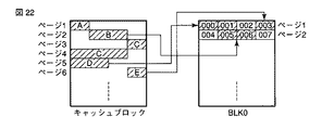
本実施形態に係るメモリシステムであると、ページバッファ31内のデータがページサイズよりも小さい場合には、それまでにデータを書き込んでいたメモリブロックBLKとは異なるメモリブロックBLKに書き込んでいる。すなわち、ページバッファ内のデータがページサイズに達するまで書き込み動作を待つ必要が無い。従って、書き込み速度を向上出来る。
(2)ページサイズ未満のデータの集約を簡便にし、高速化出来る。
本実施形態に係るメモリシステムでは、ページバッファ31とデータキャッシュ33との間で、ページ単位未満の単位でデータの授受を行っている。従って、データの集約を簡便にし、データの集約速度を高速化出来る。
(3)データの集約処理を効率化出来る。
本実施形態に係るメモリシステムであると、ページバッファ31とデータキャッシュ33との間におけるページ単位未満の単位でのデータの授受を利用して、データの書き込み時にデータの集約を行っている。データの集約処理を効率的に行うことが出来る。
Claims (5)
- ページ単位でデータを一括して書き込み、前記ページを複数含み且つ各々がデータの消去単位となる複数のメモリブロックを備えた不揮発性半導体メモリと、
前記不揮発性メモリに対して第1書き込み命令、第1ロウアドレス、書き込みデータ、及び第2書き込み命令を順次出力し、且つ出力した前記第1ロウアドレスの変更命令と、該第1ロウアドレスとは異なる第2ロウアドレスとを発行するコントローラと
を具備し、前記第1書き込み命令は、前記不揮発性半導体メモリに対して、データの書き込み動作が開始されることを認識させる命令であり、
前記第2書き込み命令は、前記不揮発性半導体メモリに対して前記書き込みデータを前記メモリブロックに書き込ませる命令であり、
前記不揮発性半導体メモリは、前記変更命令が発行されない際には前記第1ロウアドレスに対応する前記ページに前記書き込みデータを書き込み、前記変更命令が発行された際には、前記書き込みデータを再度受信することなく、前記第2ロウアドレスに対応する前記ページに前記書き込みデータを書き込む
ことを特徴とするメモリシステム。 - 前記コントローラは、前記書き込みデータのデータサイズがページサイズ未満である場合に、前記変更命令及び前記第2ロウアドレスを発行し、
前記第2ロウアドレスは、前記第1ロウアドレスとは異なる前記メモリブロック内の前記ページに対応する
ことを特徴とする請求項1記載のメモリシステム。 - 前記コントローラは、前記変更命令を発行する際には、前記書き込みデータを前記不揮発性半導体メモリへ出力した後、前記変更命令及び前記第2ロウアドレスを順次、前記不揮発性半導体メモリへ出力し、
前記第2書き込み命令は、前記第2ロウアドレスが出力された後に、前記不揮発性半導体メモリへ出力される
ことを特徴とする請求項1記載のメモリシステム。 - 前記コントローラは、ホスト機器から前記データの書き込みアクセスの終了または中断命令を受信した際に、前記データのデータサイズがページサイズ未満であるか否かを判定する
ことを特徴とする請求項2記載のメモリシステム。 - 前記書き込みデータは、FATファイルシステムにおける管理データである
ことを特徴とする請求項1記載のメモリシステム。
Priority Applications (6)
| Application Number | Priority Date | Filing Date | Title |
|---|---|---|---|
| JP2006182631A JP5002201B2 (ja) | 2006-06-30 | 2006-06-30 | メモリシステム |
| US11/770,344 US7937523B2 (en) | 2006-06-30 | 2007-06-28 | Memory system with nonvolatile semiconductor memory |
| KR1020070064437A KR100884429B1 (ko) | 2006-06-30 | 2007-06-28 | 불휘발성 반도체 메모리를 구비하는 메모리 시스템 |
| TW096123646A TWI358020B (en) | 2006-06-30 | 2007-06-29 | Memory system with nonvolatile semiconductor memor |
| CN2007101269602A CN101097543B (zh) | 2006-06-30 | 2007-07-02 | 具备非易失性半导体存储器的存储器系统 |
| US13/078,647 US20110185225A1 (en) | 2006-06-30 | 2011-04-01 | Memory system with nonvolatile semiconductor memory |
Applications Claiming Priority (1)
| Application Number | Priority Date | Filing Date | Title |
|---|---|---|---|
| JP2006182631A JP5002201B2 (ja) | 2006-06-30 | 2006-06-30 | メモリシステム |
Publications (2)
| Publication Number | Publication Date |
|---|---|
| JP2008009942A JP2008009942A (ja) | 2008-01-17 |
| JP5002201B2 true JP5002201B2 (ja) | 2012-08-15 |
Family
ID=39011388
Family Applications (1)
| Application Number | Title | Priority Date | Filing Date |
|---|---|---|---|
| JP2006182631A Expired - Fee Related JP5002201B2 (ja) | 2006-06-30 | 2006-06-30 | メモリシステム |
Country Status (5)
| Country | Link |
|---|---|
| US (2) | US7937523B2 (ja) |
| JP (1) | JP5002201B2 (ja) |
| KR (1) | KR100884429B1 (ja) |
| CN (1) | CN101097543B (ja) |
| TW (1) | TWI358020B (ja) |
Families Citing this family (39)
| Publication number | Priority date | Publication date | Assignee | Title |
|---|---|---|---|---|
| FI103329B1 (fi) * | 1997-12-22 | 1999-06-15 | Nordberg Lokomo Oy | Tapa leukamurskaimen kulutusleuan kiinnittämiseksi ja leukamurskain |
| WO2008102610A1 (ja) * | 2007-02-23 | 2008-08-28 | Panasonic Corporation | メモリコントローラ、不揮発性記憶装置、及び不揮発性記憶システム |
| JP5032155B2 (ja) * | 2007-03-02 | 2012-09-26 | 株式会社東芝 | 不揮発性半導体記憶装置、及び不揮発性半導体記憶システム |
| US7962683B2 (en) * | 2007-08-15 | 2011-06-14 | Silicon Motion, Inc. | Flash memory, and method for operating a flash memory |
| US8185685B2 (en) | 2007-12-14 | 2012-05-22 | Hitachi Global Storage Technologies Netherlands B.V. | NAND flash module replacement for DRAM module |
| JP4653817B2 (ja) * | 2008-03-01 | 2011-03-16 | 株式会社東芝 | メモリシステム |
| JP4592774B2 (ja) * | 2008-03-01 | 2010-12-08 | 株式会社東芝 | メモリシステム |
| KR101067457B1 (ko) | 2008-03-01 | 2011-09-27 | 가부시끼가이샤 도시바 | 메모리 시스템 |
| TWI385519B (zh) * | 2008-04-18 | 2013-02-11 | Phison Electronics Corp | 資料寫入方法及使用此方法的快閃儲存系統與其控制器 |
| JP4649503B2 (ja) * | 2008-08-13 | 2011-03-09 | 株式会社東芝 | 半導体装置 |
| TWI413984B (zh) * | 2008-10-16 | 2013-11-01 | Silicon Motion Inc | 快閃記憶體裝置以及資料更新方法 |
| US8549209B2 (en) * | 2008-11-04 | 2013-10-01 | Mosaid Technologies Incorporated | Bridging device having a configurable virtual page size |
| US8244960B2 (en) * | 2009-01-05 | 2012-08-14 | Sandisk Technologies Inc. | Non-volatile memory and method with write cache partition management methods |
| US8094500B2 (en) * | 2009-01-05 | 2012-01-10 | Sandisk Technologies Inc. | Non-volatile memory and method with write cache partitioning |
| US8700840B2 (en) * | 2009-01-05 | 2014-04-15 | SanDisk Technologies, Inc. | Nonvolatile memory with write cache having flush/eviction methods |
| CN101859605B (zh) * | 2009-04-10 | 2013-05-01 | 国民技术股份有限公司 | 一种使用瑕疵闪存的方法 |
| TWI435215B (zh) * | 2009-08-26 | 2014-04-21 | Phison Electronics Corp | 下達讀取指令與資料讀取方法、控制器與儲存系統 |
| JP5657242B2 (ja) * | 2009-12-09 | 2015-01-21 | 株式会社東芝 | 半導体装置及びメモリシステム |
| TWI416331B (zh) * | 2009-12-23 | 2013-11-21 | Phison Electronics Corp | 用於快閃記憶體的資料寫入方法及其控制器與儲存裝置 |
| JP5708216B2 (ja) * | 2011-05-09 | 2015-04-30 | ソニー株式会社 | フラッシュメモリ装置、メモリ制御装置、メモリ制御方法、ストレージシステム |
| JP5768654B2 (ja) * | 2011-10-25 | 2015-08-26 | ソニー株式会社 | 記憶制御装置、記憶装置、情報処理システム、および、記憶制御方法 |
| CN103680610A (zh) * | 2012-09-03 | 2014-03-26 | 北京兆易创新科技股份有限公司 | 差分存储NAND Flash存储器写操作的方法及装置 |
| KR102133573B1 (ko) | 2013-02-26 | 2020-07-21 | 삼성전자주식회사 | 반도체 메모리 및 반도체 메모리를 포함하는 메모리 시스템 |
| EP3333853A1 (en) * | 2013-03-07 | 2018-06-13 | Charles I. Peddle | High speed flash controllers |
| US9069660B2 (en) * | 2013-03-15 | 2015-06-30 | Apple Inc. | Systems and methods for writing to high-capacity memory |
| US20150095551A1 (en) * | 2013-09-30 | 2015-04-02 | Micron Technology, Inc. | Volatile memory architecutre in non-volatile memory devices and related controllers |
| JP6107625B2 (ja) * | 2013-12-02 | 2017-04-05 | ソニー株式会社 | 記憶制御装置、記憶装置、情報処理システムおよびその記憶制御方法 |
| US9460019B2 (en) * | 2014-06-26 | 2016-10-04 | Intel Corporation | Sending packets using optimized PIO write sequences without SFENCEs |
| JP2016028319A (ja) * | 2014-07-08 | 2016-02-25 | 富士通株式会社 | アクセス制御プログラム、アクセス制御装置及びアクセス制御方法 |
| KR20170008339A (ko) * | 2015-07-13 | 2017-01-24 | 에스케이하이닉스 주식회사 | 메모리 시스템 및 메모리 시스템의 동작 방법 |
| US11809727B1 (en) * | 2016-04-27 | 2023-11-07 | Pure Storage, Inc. | Predicting failures in a storage system that includes a plurality of storage devices |
| US11112990B1 (en) | 2016-04-27 | 2021-09-07 | Pure Storage, Inc. | Managing storage device evacuation |
| CN109582235B (zh) * | 2018-11-27 | 2021-12-21 | 杭州宏杉科技股份有限公司 | 管理元数据存储方法及装置 |
| CN109815711B (zh) * | 2018-12-21 | 2020-12-25 | 航天信息股份有限公司 | 一种存储设备、数据存储方法和数据读取方法 |
| KR102918292B1 (ko) * | 2020-05-19 | 2026-01-28 | 에스케이하이닉스 주식회사 | 저장 장치 및 그 동작 방법 |
| JP7500365B2 (ja) | 2020-09-14 | 2024-06-17 | キオクシア株式会社 | メモリシステム |
| CN113409849A (zh) * | 2021-05-21 | 2021-09-17 | 芯天下技术股份有限公司 | 一种降低编程功耗的方法、装置、存储介质和终端 |
| CN113409852A (zh) * | 2021-06-17 | 2021-09-17 | 芯天下技术股份有限公司 | 一种提高闪存编程效率的方法、装置、存储介质和终端 |
| CN113409850A (zh) * | 2021-06-17 | 2021-09-17 | 芯天下技术股份有限公司 | 一种提高编程效率的方法、装置、存储介质和终端 |
Family Cites Families (22)
| Publication number | Priority date | Publication date | Assignee | Title |
|---|---|---|---|---|
| US4680647A (en) * | 1983-09-26 | 1987-07-14 | Pioneer Electronic Corporation | Method for recording and reproducing video format signal |
| US5371885A (en) * | 1989-08-29 | 1994-12-06 | Microsoft Corporation | High performance file system |
| FR2710445B1 (fr) * | 1993-09-20 | 1995-11-03 | Sgs Thomson Microelectronics | Circuit de redondance dynamique pour mémoire en circuit intégré. |
| GB2285524B (en) | 1994-01-11 | 1998-02-04 | Advanced Risc Mach Ltd | Data memory and processor bus |
| US6047352A (en) * | 1996-10-29 | 2000-04-04 | Micron Technology, Inc. | Memory system, method and predecoding circuit operable in different modes for selectively accessing multiple blocks of memory cells for simultaneous writing or erasure |
| JPH11224492A (ja) | 1997-11-06 | 1999-08-17 | Toshiba Corp | 半導体記憶装置、不揮発性半導体記憶装置及びフラッシュメモリ |
| JPH11242630A (ja) * | 1997-12-26 | 1999-09-07 | Mitsubishi Electric Corp | ベースバンドic |
| JP2000067582A (ja) * | 1998-08-14 | 2000-03-03 | Texas Instr Inc <Ti> | メモリシステムおよび電子装置の動作方法 |
| US6449193B1 (en) * | 2000-12-28 | 2002-09-10 | Texas Instruments Incorporated | Burst access memory system |
| JP3979486B2 (ja) | 2001-09-12 | 2007-09-19 | 株式会社ルネサステクノロジ | 不揮発性記憶装置およびデータ格納方法 |
| US6850438B2 (en) * | 2002-07-05 | 2005-02-01 | Aplus Flash Technology, Inc. | Combination nonvolatile memory using unified technology with byte, page and block write and simultaneous read and write operations |
| US6944063B2 (en) * | 2003-01-28 | 2005-09-13 | Sandisk Corporation | Non-volatile semiconductor memory with large erase blocks storing cycle counts |
| JP2005063038A (ja) | 2003-08-08 | 2005-03-10 | Sony Corp | データ処理装置、その方法、そのプログラムおよび記録媒体 |
| CN100349138C (zh) | 2003-08-08 | 2007-11-14 | 倚天资讯股份有限公司 | 非挥发性存储器存取系统及其循环使用存取空间方法 |
| KR101087906B1 (ko) | 2003-11-18 | 2011-11-30 | 파나소닉 주식회사 | 파일기록장치 |
| JP2005332125A (ja) | 2004-05-19 | 2005-12-02 | Victor Co Of Japan Ltd | メモリコントローラ及び共有メモリシステム |
| JP4253272B2 (ja) * | 2004-05-27 | 2009-04-08 | 株式会社東芝 | メモリカード、半導体装置、及び半導体メモリの制御方法 |
| KR100568115B1 (ko) * | 2004-06-30 | 2006-04-05 | 삼성전자주식회사 | 점진적 머지 방법 및 그것을 이용한 메모리 시스템 |
| JP4713867B2 (ja) * | 2004-09-22 | 2011-06-29 | 株式会社東芝 | メモリコントローラ,メモリ装置及びメモリコントローラの制御方法 |
| US7366826B2 (en) * | 2004-12-16 | 2008-04-29 | Sandisk Corporation | Non-volatile memory and method with multi-stream update tracking |
| JP4738038B2 (ja) | 2005-03-25 | 2011-08-03 | 株式会社東芝 | メモリカード |
| KR100634457B1 (ko) * | 2005-07-04 | 2006-10-16 | 삼성전자주식회사 | 단일의 페이지 버퍼 구조로 멀티-비트 및 단일-비트프로그램 동작을 수행하는 플래시 메모리 장치 |
-
2006
- 2006-06-30 JP JP2006182631A patent/JP5002201B2/ja not_active Expired - Fee Related
-
2007
- 2007-06-28 KR KR1020070064437A patent/KR100884429B1/ko not_active Expired - Fee Related
- 2007-06-28 US US11/770,344 patent/US7937523B2/en not_active Expired - Fee Related
- 2007-06-29 TW TW096123646A patent/TWI358020B/zh not_active IP Right Cessation
- 2007-07-02 CN CN2007101269602A patent/CN101097543B/zh not_active Expired - Fee Related
-
2011
- 2011-04-01 US US13/078,647 patent/US20110185225A1/en not_active Abandoned
Also Published As
| Publication number | Publication date |
|---|---|
| TWI358020B (en) | 2012-02-11 |
| KR100884429B1 (ko) | 2009-02-19 |
| CN101097543B (zh) | 2010-06-23 |
| US20080046639A1 (en) | 2008-02-21 |
| US7937523B2 (en) | 2011-05-03 |
| CN101097543A (zh) | 2008-01-02 |
| TW200819976A (en) | 2008-05-01 |
| US20110185225A1 (en) | 2011-07-28 |
| KR20080002646A (ko) | 2008-01-04 |
| JP2008009942A (ja) | 2008-01-17 |
Similar Documents
| Publication | Publication Date | Title |
|---|---|---|
| JP5002201B2 (ja) | メモリシステム | |
| KR100874998B1 (ko) | 반도체 집적 회로 장치의 데이터 기록 방식 | |
| US11630766B2 (en) | Memory system and operating method thereof | |
| US8386698B2 (en) | Data accessing method for flash memory and storage system and controller using the same | |
| US7814264B2 (en) | Memory card, semiconductor device, and method of controlling semiconductor memory | |
| US8356134B2 (en) | Memory device with non-volatile memory buffer | |
| US8055873B2 (en) | Data writing method for flash memory, and controller and system using the same | |
| JP4649503B2 (ja) | 半導体装置 | |
| US20100042774A1 (en) | Block management method for flash memory, and storage system and controller using the same | |
| US20100057979A1 (en) | Data transmission method for flash memory and flash memory storage system and controller using the same | |
| US9619380B2 (en) | Data writing method, memory control circuit unit and memory storage apparatus | |
| JP2008009919A (ja) | カードコントローラ | |
| US11803223B2 (en) | Open channel solid state drive, nonvolatile memory system including the same and method of power loss protection of open channel solid state drive | |
| US7404031B2 (en) | Memory card, nonvolatile semiconductor memory, and method of controlling semiconductor memory | |
| KR100882740B1 (ko) | 맵 히스토리 기반의 불휘발성 메모리의 매핑 방법 및 저장장치 | |
| JP4373943B2 (ja) | メモリコントローラ、フラッシュメモリシステム及びフラッシュメモリの制御方法 | |
| JP4697146B2 (ja) | メモリコントローラ及びメモリコントローラを備えるフラッシュメモリシステム、並びにフラッシュメモリの制御方法 | |
| US9146861B2 (en) | Memory address management method, memory controller and memory storage device | |
| US6898680B2 (en) | Minimization of overhead of non-volatile memory operation | |
| JP4177292B2 (ja) | メモリンコントローラ、フラッシュメモリシステム及びフラッシュメモリの制御方法 | |
| JP4334331B2 (ja) | フラッシュメモリのアクセス制御方法 | |
| JP2005292925A (ja) | メモリコントローラ、フラッシュメモリシステム、並びに、フラッシュメモリの制御方法 | |
| JP2008084184A (ja) | メモリコントローラ | |
| KR20090046568A (ko) | 플래시 메모리 시스템 및 그것의 쓰기 방법 | |
| JP4177301B2 (ja) | メモリコントローラ、フラッシュメモリシステム及びフラッシュメモリの制御方法 |
Legal Events
| Date | Code | Title | Description |
|---|---|---|---|
| A621 | Written request for application examination |
Free format text: JAPANESE INTERMEDIATE CODE: A621 Effective date: 20090209 |
|
| A131 | Notification of reasons for refusal |
Free format text: JAPANESE INTERMEDIATE CODE: A131 Effective date: 20111025 |
|
| A521 | Request for written amendment filed |
Free format text: JAPANESE INTERMEDIATE CODE: A523 Effective date: 20111202 |
|
| TRDD | Decision of grant or rejection written | ||
| A01 | Written decision to grant a patent or to grant a registration (utility model) |
Free format text: JAPANESE INTERMEDIATE CODE: A01 Effective date: 20120424 |
|
| A01 | Written decision to grant a patent or to grant a registration (utility model) |
Free format text: JAPANESE INTERMEDIATE CODE: A01 |
|
| A61 | First payment of annual fees (during grant procedure) |
Free format text: JAPANESE INTERMEDIATE CODE: A61 Effective date: 20120521 |
|
| FPAY | Renewal fee payment (event date is renewal date of database) |
Free format text: PAYMENT UNTIL: 20150525 Year of fee payment: 3 |
|
| RD04 | Notification of resignation of power of attorney |
Free format text: JAPANESE INTERMEDIATE CODE: A7424 Effective date: 20120529 |
|
| A072 | Dismissal of procedure [no reply to invitation to correct request for examination] |
Free format text: JAPANESE INTERMEDIATE CODE: A072 Effective date: 20121009 |
|
| LAPS | Cancellation because of no payment of annual fees |