JP5018245B2 - アナログスイッチ - Google Patents
アナログスイッチ Download PDFInfo
- Publication number
- JP5018245B2 JP5018245B2 JP2007144355A JP2007144355A JP5018245B2 JP 5018245 B2 JP5018245 B2 JP 5018245B2 JP 2007144355 A JP2007144355 A JP 2007144355A JP 2007144355 A JP2007144355 A JP 2007144355A JP 5018245 B2 JP5018245 B2 JP 5018245B2
- Authority
- JP
- Japan
- Prior art keywords
- potential
- gate
- mosfet
- switch
- well
- Prior art date
- Legal status (The legal status is an assumption and is not a legal conclusion. Google has not performed a legal analysis and makes no representation as to the accuracy of the status listed.)
- Expired - Fee Related
Links
Images




Classifications
-
- H—ELECTRICITY
- H03—ELECTRONIC CIRCUITRY
- H03K—PULSE TECHNIQUE
- H03K17/00—Electronic switching or gating, i.e. not by contact-making and –breaking
- H03K17/04—Modifications for accelerating switching
- H03K17/041—Modifications for accelerating switching without feedback from the output circuit to the control circuit
- H03K17/0416—Modifications for accelerating switching without feedback from the output circuit to the control circuit by measures taken in the output circuit
- H03K17/04163—Modifications for accelerating switching without feedback from the output circuit to the control circuit by measures taken in the output circuit in field-effect transistor switches
-
- H—ELECTRICITY
- H03—ELECTRONIC CIRCUITRY
- H03K—PULSE TECHNIQUE
- H03K17/00—Electronic switching or gating, i.e. not by contact-making and –breaking
- H03K17/04—Modifications for accelerating switching
- H03K17/042—Modifications for accelerating switching by feedback from the output circuit to the control circuit
- H03K17/04206—Modifications for accelerating switching by feedback from the output circuit to the control circuit in field-effect transistor switches
Landscapes
- Electronic Switches (AREA)
Description
に示される。しかし、この回路はウェル電位を制御する回路を通してウェル−基板間の容量が見えることについて配慮されておらず、またゲート電位も固定された電位を与えているため、入出力端から見える容量を小さくすることが困難であることを本願発明者等は見いだした。
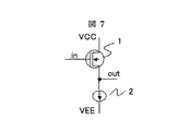
図7に実施例1におけるウェル電位用レベルシフトバッファ2の回路例を示す。端子inを入力とし、NMOS1と電流源2から構成されるソースフォロアによって端子outに出力する。
VEE…負電源、
BULK…基板電位、
WEL…ウェル電位、
GATE…ゲート電位、
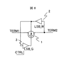
TERM1…アナログスイッチ端子1、
TERM2…アナログスイッチ端子2、
CTRL…アナログスイッチのON/OFFの制御端子、
LSB_W…ウェル電位用レベルシフトバッファ、
LSB_G…ゲート電位用レベルシフトバッファ、
SEL…電位セレクタ、
DUT…テスタにおける測定対象物、
PINELECTRONICS…LSIテスタにおいてDUTへの電圧・電流印加とDUTの出力電圧・電流の測定する部品、
DRIVER…DUTへAC若しくはDCの電圧を印加する部品、
COMPARATOR…DUTのAC若しくはDCの出力電圧を設定電圧と比較する部品、
LOAD…DUTへの電流負荷を供給する部品、
DCL…DRIVERとCOMPARATORとLOADの総称、
PMU…DUTに電圧・電流の印加とDUTの入出力電圧・電流を基準値と比較する部品。
Claims (2)
- ソース、ドレイン、ゲート、およびウェルを端子として有するMOSFETと、
前記ソースおよび前記ドレインのいずれか一方に接続されたスイッチ入力端子および他方に接続されたスイッチ出力端子と、
前記ゲートに直接または間接的に接続され、前記スイッチ入力端子と前記スイッチ出力端子の間の電気的導通をON状態またはOFF状態に保持する電位が印加されるスイッチ制御端子と、
前記スイッチ出力端子に入力端子が直接または間接的に接続され、かつ、前記ゲートおよび前記ウェルの少なくともいずれか一方に出力端子が接続された、前記スイッチ出力端子の電位に前記ゲートの電位および前記ウェルの電位の少なくともいずれか一方を追随させるためのレベルシフトバッファとを具備し、
前記レベルシフトバッファは、前記MOSFETの前記ソースおよび前記ドレインのいずれか一方の電位に前記ゲートの電位を追随させるゲート電位用レベルシフトバッファであり、
前記MOSFETの前記ソースおよび前記ドレインの両方の電位から、P型の場合は高電位を、N型の場合は低電位を、それぞれ選択するセレクタを更に具備して成り、
前記ゲート電位用レベルシフトバッファは前記セレクタによって選択された電位に前記ゲートの電位を追随させる機能を有し
て成ることを特徴とするアナログスイッチ。 - 請求項1において、
前記MOSFETは、P型若しくはN型の単体MOSFET、又はP型MOSFETとN型MOSFETとの並列接続で構成されることを特徴とするアナログスイッチ。
Priority Applications (2)
| Application Number | Priority Date | Filing Date | Title |
|---|---|---|---|
| JP2007144355A JP5018245B2 (ja) | 2007-05-31 | 2007-05-31 | アナログスイッチ |
| US12/128,637 US8008963B2 (en) | 2007-05-31 | 2008-05-29 | Analog switch |
Applications Claiming Priority (1)
| Application Number | Priority Date | Filing Date | Title |
|---|---|---|---|
| JP2007144355A JP5018245B2 (ja) | 2007-05-31 | 2007-05-31 | アナログスイッチ |
Publications (2)
| Publication Number | Publication Date |
|---|---|
| JP2008301144A JP2008301144A (ja) | 2008-12-11 |
| JP5018245B2 true JP5018245B2 (ja) | 2012-09-05 |
Family
ID=40087161
Family Applications (1)
| Application Number | Title | Priority Date | Filing Date |
|---|---|---|---|
| JP2007144355A Expired - Fee Related JP5018245B2 (ja) | 2007-05-31 | 2007-05-31 | アナログスイッチ |
Country Status (2)
| Country | Link |
|---|---|
| US (1) | US8008963B2 (ja) |
| JP (1) | JP5018245B2 (ja) |
Families Citing this family (11)
| Publication number | Priority date | Publication date | Assignee | Title |
|---|---|---|---|---|
| US8094576B2 (en) | 2007-08-07 | 2012-01-10 | Net Optic, Inc. | Integrated switch tap arrangement with visual display arrangement and methods thereof |
| JP5431992B2 (ja) * | 2010-02-09 | 2014-03-05 | セイコーインスツル株式会社 | トランスミッションゲート及び半導体装置 |
| US9813448B2 (en) | 2010-02-26 | 2017-11-07 | Ixia | Secured network arrangement and methods thereof |
| US9749261B2 (en) * | 2010-02-28 | 2017-08-29 | Ixia | Arrangements and methods for minimizing delay in high-speed taps |
| US8880014B2 (en) * | 2010-06-07 | 2014-11-04 | Skyworks Solutions, Inc. | CMOS RF switch device and method for biasing the same |
| KR101863973B1 (ko) * | 2013-07-08 | 2018-06-04 | 매그나칩 반도체 유한회사 | 씨모스 아날로그 스위치 회로 |
| US10382036B2 (en) * | 2015-01-29 | 2019-08-13 | Qualcomm Incorporated | High voltage switch |
| US9998213B2 (en) | 2016-07-29 | 2018-06-12 | Keysight Technologies Singapore (Holdings) Pte. Ltd. | Network tap with battery-assisted and programmable failover |
| US10312906B2 (en) | 2016-09-16 | 2019-06-04 | Asahi Kasei Microdevices Corporation | Switch apparatus |
| TWI694729B (zh) * | 2018-06-19 | 2020-05-21 | 瑞昱半導體股份有限公司 | 開關電路 |
| CN109245752B (zh) * | 2018-10-22 | 2024-02-27 | 上海艾为电子技术股份有限公司 | 一种调整电路和模拟开关 |
Family Cites Families (11)
| Publication number | Priority date | Publication date | Assignee | Title |
|---|---|---|---|---|
| JPS6129215A (ja) * | 1984-07-20 | 1986-02-10 | Hitachi Ltd | アナログ・スイツチ回路 |
| JP2551925B2 (ja) * | 1987-11-24 | 1996-11-06 | 株式会社共和電業 | 接合容量キャンセル式fetスイッチ回路 |
| US5084634A (en) * | 1990-10-24 | 1992-01-28 | Burr-Brown Corporation | Dynamic input sampling switch for CDACS |
| JPH06169247A (ja) | 1992-11-30 | 1994-06-14 | New Japan Radio Co Ltd | アナログスイッチ |
| FR2738424B1 (fr) * | 1995-09-05 | 1997-11-21 | Sgs Thomson Microelectronics | Interrupteur analogique basse tension |
| JP3258930B2 (ja) * | 1997-04-24 | 2002-02-18 | 東芝マイクロエレクトロニクス株式会社 | トランスミッション・ゲート |
| US6163199A (en) * | 1999-01-29 | 2000-12-19 | Fairchild Semiconductor Corp. | Overvoltage/undervoltage tolerant transfer gate |
| JP2001110195A (ja) * | 1999-10-08 | 2001-04-20 | Agilent Technologies Japan Ltd | トラックアンドホールド回路 |
| JP3765982B2 (ja) | 2000-08-15 | 2006-04-12 | 株式会社東芝 | トレラント機能付きアナログスイッチ回路 |
| JP2003163589A (ja) * | 2001-11-22 | 2003-06-06 | Toshiba Corp | トレラント機能付きアナログスイッチ回路 |
| JP4487726B2 (ja) * | 2004-10-28 | 2010-06-23 | 株式会社デンソー | アナログスイッチおよびスイッチトキャパシタフィルタ |
-
2007
- 2007-05-31 JP JP2007144355A patent/JP5018245B2/ja not_active Expired - Fee Related
-
2008
- 2008-05-29 US US12/128,637 patent/US8008963B2/en not_active Expired - Fee Related
Also Published As
| Publication number | Publication date |
|---|---|
| US8008963B2 (en) | 2011-08-30 |
| JP2008301144A (ja) | 2008-12-11 |
| US20080296685A1 (en) | 2008-12-04 |
Similar Documents
| Publication | Publication Date | Title |
|---|---|---|
| JP5018245B2 (ja) | アナログスイッチ | |
| US8354873B2 (en) | Transmission gate and semiconductor device | |
| JP4128545B2 (ja) | サンプリングスイッチ | |
| US8212604B2 (en) | T switch with high off state isolation | |
| US9843321B2 (en) | System and method for a pre-driver circuit | |
| JP2003143004A (ja) | レベルシフタ回路 | |
| US20150036252A1 (en) | Semiconductor driving device and semiconductor device | |
| WO2013142238A1 (en) | Bi-directional switch using series connected n-type mos devices in parallel with series connected p-type mos devices | |
| US8314638B2 (en) | Comparator circuit | |
| CN102622024A (zh) | 位准转换电路 | |
| US10586605B2 (en) | Sample hold circuit | |
| US7501874B2 (en) | Level shift circuit | |
| US8629721B2 (en) | Output stage formed inside and on top of an SOI-type substrate | |
| US10348305B2 (en) | Level shift circuit | |
| US7492210B2 (en) | Voltage selection circuit | |
| JP4672575B2 (ja) | パワーデバイスの駆動回路 | |
| US10312913B2 (en) | Level shifter | |
| US9838015B2 (en) | Apparatus for performing level shift control in an electronic device with aid of parallel paths controlled by different control signals for current control purposes | |
| KR20050085862A (ko) | 스위칭 회로 | |
| US20250373247A1 (en) | Analog switch | |
| US20240125823A1 (en) | Current sensor | |
| JP2010045522A (ja) | 半導体装置 | |
| US20100102850A1 (en) | Semiconductor device | |
| JP2007189507A (ja) | 高周波スイッチ回路 | |
| JP2009260455A (ja) | レベル変換回路および画像表示装置 |
Legal Events
| Date | Code | Title | Description |
|---|---|---|---|
| A621 | Written request for application examination |
Free format text: JAPANESE INTERMEDIATE CODE: A621 Effective date: 20100305 |
|
| A977 | Report on retrieval |
Free format text: JAPANESE INTERMEDIATE CODE: A971007 Effective date: 20120227 |
|
| A131 | Notification of reasons for refusal |
Free format text: JAPANESE INTERMEDIATE CODE: A131 Effective date: 20120313 |
|
| A521 | Request for written amendment filed |
Free format text: JAPANESE INTERMEDIATE CODE: A523 Effective date: 20120420 |
|
| TRDD | Decision of grant or rejection written | ||
| A01 | Written decision to grant a patent or to grant a registration (utility model) |
Free format text: JAPANESE INTERMEDIATE CODE: A01 Effective date: 20120515 |
|
| A01 | Written decision to grant a patent or to grant a registration (utility model) |
Free format text: JAPANESE INTERMEDIATE CODE: A01 |
|
| A61 | First payment of annual fees (during grant procedure) |
Free format text: JAPANESE INTERMEDIATE CODE: A61 Effective date: 20120528 |
|
| FPAY | Renewal fee payment (event date is renewal date of database) |
Free format text: PAYMENT UNTIL: 20150622 Year of fee payment: 3 |
|
| LAPS | Cancellation because of no payment of annual fees |