JP5065417B2 - 単純マトリクス型の表示素子を有する表示装置 - Google Patents
単純マトリクス型の表示素子を有する表示装置 Download PDFInfo
- Publication number
- JP5065417B2 JP5065417B2 JP2009547818A JP2009547818A JP5065417B2 JP 5065417 B2 JP5065417 B2 JP 5065417B2 JP 2009547818 A JP2009547818 A JP 2009547818A JP 2009547818 A JP2009547818 A JP 2009547818A JP 5065417 B2 JP5065417 B2 JP 5065417B2
- Authority
- JP
- Japan
- Prior art keywords
- signal
- liquid crystal
- display
- pulse
- driver
- Prior art date
- Legal status (The legal status is an assumption and is not a legal conclusion. Google has not performed a legal analysis and makes no representation as to the accuracy of the status listed.)
- Active
Links
Images






Classifications
-
- G—PHYSICS
- G09—EDUCATION; CRYPTOGRAPHY; DISPLAY; ADVERTISING; SEALS
- G09G—ARRANGEMENTS OR CIRCUITS FOR CONTROL OF INDICATING DEVICES USING STATIC MEANS TO PRESENT VARIABLE INFORMATION
- G09G3/00—Control arrangements or circuits, of interest only in connection with visual indicators other than cathode-ray tubes
- G09G3/20—Control arrangements or circuits, of interest only in connection with visual indicators other than cathode-ray tubes for presentation of an assembly of a number of characters, e.g. a page, by composing the assembly by combination of individual elements arranged in a matrix no fixed position being assigned to or needed to be assigned to the individual characters or partial characters
- G09G3/34—Control arrangements or circuits, of interest only in connection with visual indicators other than cathode-ray tubes for presentation of an assembly of a number of characters, e.g. a page, by composing the assembly by combination of individual elements arranged in a matrix no fixed position being assigned to or needed to be assigned to the individual characters or partial characters by control of light from an independent source
- G09G3/36—Control arrangements or circuits, of interest only in connection with visual indicators other than cathode-ray tubes for presentation of an assembly of a number of characters, e.g. a page, by composing the assembly by combination of individual elements arranged in a matrix no fixed position being assigned to or needed to be assigned to the individual characters or partial characters by control of light from an independent source using liquid crystals
- G09G3/3611—Control of matrices with row and column drivers
- G09G3/3622—Control of matrices with row and column drivers using a passive matrix
- G09G3/3629—Control of matrices with row and column drivers using a passive matrix using liquid crystals having memory effects, e.g. ferroelectric liquid crystals
-
- G—PHYSICS
- G09—EDUCATION; CRYPTOGRAPHY; DISPLAY; ADVERTISING; SEALS
- G09G—ARRANGEMENTS OR CIRCUITS FOR CONTROL OF INDICATING DEVICES USING STATIC MEANS TO PRESENT VARIABLE INFORMATION
- G09G2300/00—Aspects of the constitution of display devices
- G09G2300/02—Composition of display devices
- G09G2300/023—Display panel composed of stacked panels
-
- G—PHYSICS
- G09—EDUCATION; CRYPTOGRAPHY; DISPLAY; ADVERTISING; SEALS
- G09G—ARRANGEMENTS OR CIRCUITS FOR CONTROL OF INDICATING DEVICES USING STATIC MEANS TO PRESENT VARIABLE INFORMATION
- G09G2300/00—Aspects of the constitution of display devices
- G09G2300/04—Structural and physical details of display devices
- G09G2300/0469—Details of the physics of pixel operation
- G09G2300/0478—Details of the physics of pixel operation related to liquid crystal pixels
- G09G2300/0482—Use of memory effects in nematic liquid crystals
- G09G2300/0486—Cholesteric liquid crystals, including chiral-nematic liquid crystals, with transitions between focal conic, planar, and homeotropic states
-
- G—PHYSICS
- G09—EDUCATION; CRYPTOGRAPHY; DISPLAY; ADVERTISING; SEALS
- G09G—ARRANGEMENTS OR CIRCUITS FOR CONTROL OF INDICATING DEVICES USING STATIC MEANS TO PRESENT VARIABLE INFORMATION
- G09G2310/00—Command of the display device
- G09G2310/02—Addressing, scanning or driving the display screen or processing steps related thereto
- G09G2310/0264—Details of driving circuits
- G09G2310/0278—Details of driving circuits arranged to drive both scan and data electrodes
-
- G—PHYSICS
- G09—EDUCATION; CRYPTOGRAPHY; DISPLAY; ADVERTISING; SEALS
- G09G—ARRANGEMENTS OR CIRCUITS FOR CONTROL OF INDICATING DEVICES USING STATIC MEANS TO PRESENT VARIABLE INFORMATION
- G09G2320/00—Control of display operating conditions
- G09G2320/02—Improving the quality of display appearance
- G09G2320/0204—Compensation of DC component across the pixels in flat panels
-
- G—PHYSICS
- G09—EDUCATION; CRYPTOGRAPHY; DISPLAY; ADVERTISING; SEALS
- G09G—ARRANGEMENTS OR CIRCUITS FOR CONTROL OF INDICATING DEVICES USING STATIC MEANS TO PRESENT VARIABLE INFORMATION
- G09G2320/00—Control of display operating conditions
- G09G2320/02—Improving the quality of display appearance
- G09G2320/0252—Improving the response speed
-
- G—PHYSICS
- G09—EDUCATION; CRYPTOGRAPHY; DISPLAY; ADVERTISING; SEALS
- G09G—ARRANGEMENTS OR CIRCUITS FOR CONTROL OF INDICATING DEVICES USING STATIC MEANS TO PRESENT VARIABLE INFORMATION
- G09G2330/00—Aspects of power supply; Aspects of display protection and defect management
- G09G2330/02—Details of power systems and of start or stop of display operation
- G09G2330/025—Reduction of instantaneous peaks of current
-
- G—PHYSICS
- G09—EDUCATION; CRYPTOGRAPHY; DISPLAY; ADVERTISING; SEALS
- G09G—ARRANGEMENTS OR CIRCUITS FOR CONTROL OF INDICATING DEVICES USING STATIC MEANS TO PRESENT VARIABLE INFORMATION
- G09G3/00—Control arrangements or circuits, of interest only in connection with visual indicators other than cathode-ray tubes
- G09G3/20—Control arrangements or circuits, of interest only in connection with visual indicators other than cathode-ray tubes for presentation of an assembly of a number of characters, e.g. a page, by composing the assembly by combination of individual elements arranged in a matrix no fixed position being assigned to or needed to be assigned to the individual characters or partial characters
- G09G3/2007—Display of intermediate tones
- G09G3/2014—Display of intermediate tones by modulation of the duration of a single pulse during which the logic level remains constant
-
- G—PHYSICS
- G09—EDUCATION; CRYPTOGRAPHY; DISPLAY; ADVERTISING; SEALS
- G09G—ARRANGEMENTS OR CIRCUITS FOR CONTROL OF INDICATING DEVICES USING STATIC MEANS TO PRESENT VARIABLE INFORMATION
- G09G3/00—Control arrangements or circuits, of interest only in connection with visual indicators other than cathode-ray tubes
- G09G3/20—Control arrangements or circuits, of interest only in connection with visual indicators other than cathode-ray tubes for presentation of an assembly of a number of characters, e.g. a page, by composing the assembly by combination of individual elements arranged in a matrix no fixed position being assigned to or needed to be assigned to the individual characters or partial characters
- G09G3/2007—Display of intermediate tones
- G09G3/2018—Display of intermediate tones by time modulation using two or more time intervals
-
- G—PHYSICS
- G09—EDUCATION; CRYPTOGRAPHY; DISPLAY; ADVERTISING; SEALS
- G09G—ARRANGEMENTS OR CIRCUITS FOR CONTROL OF INDICATING DEVICES USING STATIC MEANS TO PRESENT VARIABLE INFORMATION
- G09G3/00—Control arrangements or circuits, of interest only in connection with visual indicators other than cathode-ray tubes
- G09G3/20—Control arrangements or circuits, of interest only in connection with visual indicators other than cathode-ray tubes for presentation of an assembly of a number of characters, e.g. a page, by composing the assembly by combination of individual elements arranged in a matrix no fixed position being assigned to or needed to be assigned to the individual characters or partial characters
- G09G3/34—Control arrangements or circuits, of interest only in connection with visual indicators other than cathode-ray tubes for presentation of an assembly of a number of characters, e.g. a page, by composing the assembly by combination of individual elements arranged in a matrix no fixed position being assigned to or needed to be assigned to the individual characters or partial characters by control of light from an independent source
- G09G3/36—Control arrangements or circuits, of interest only in connection with visual indicators other than cathode-ray tubes for presentation of an assembly of a number of characters, e.g. a page, by composing the assembly by combination of individual elements arranged in a matrix no fixed position being assigned to or needed to be assigned to the individual characters or partial characters by control of light from an independent source using liquid crystals
- G09G3/3611—Control of matrices with row and column drivers
- G09G3/3614—Control of polarity reversal in general
Landscapes
- Engineering & Computer Science (AREA)
- Chemical & Material Sciences (AREA)
- Crystallography & Structural Chemistry (AREA)
- Physics & Mathematics (AREA)
- Computer Hardware Design (AREA)
- General Physics & Mathematics (AREA)
- Theoretical Computer Science (AREA)
- Control Of Indicators Other Than Cathode Ray Tubes (AREA)
- Liquid Crystal (AREA)
- Liquid Crystal Display Device Control (AREA)
Description
同図に示すように、コレステリック液晶を利用した表示素子10は、上側基板11と、コレステリック液晶層12と、及び下側基板13と、を備えて構成されている。コレステリック液晶の動作状態には、図1Aに示すように入射光を反射することができるプレーナ状態と、図1Bに示すように入射光を透過させることができるフォーカルコニック状態とがあるが、これらの状態は、いずれも、電圧が印加されない状態、即ち無電界下においても維持される。よって、コレステリック液晶では、安定した表示状態を保持することができる。
コレステリック液晶の動作状態がプレーナ状態の時には、入射光が反射するので「明」状態となり、即ち白を表示することができる状態となる。他方、コレステリック液晶の動作状態がフォーカルコニック状態の時には、下側基板13の下に光吸収層が設置されている場合には、光が液晶層を透過すると共に、当該光吸収層によって吸収されるので、「暗」状態となり、即ち黒を表示することができる状態となる。
図2は、従来の一般的なコレステリック液晶の電圧−反射率特性を示すグラフ図である。
同図に示すグラフ図において、グラフの縦軸はコレステリック液晶の反射率(%)を表し、横軸は、コレステリック液晶を挟む電極間に所定のパルス幅で印加されるパルス電圧の電圧値(V)を表している。
また、実線で示す曲線Pは、初期状態がプレーナ状態となっているコレステリック液晶の電圧−反射率特性を示しており、また、破線で示す曲線FCは、初期状態が、入射光を透過するフォーカルコニック状態となっているコレステリック液晶の電圧−反射率特性を示すものである。
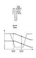
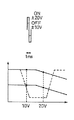
図3Aは、コレステリック液晶において、電圧パルスのパルス幅が数十msの場合のパルス応答特性を示し、図3Bは電圧パルスのパルス幅が2msの場合のパルス応答特性を示し、図3Cは電圧パルスのパルス幅が1msの場合のパルス応答特性を示すグラフ図である。 各図の上側にはコレステリック液晶に印加される電圧パルスを示し、下側には電圧−反射率特性を示している、また、グラフ図の縦軸は反射率(%)を表し、横軸は電圧(V)を表している。コレステリック液晶の駆動パルスには正極性と負極性のパルスを組み合わせて使用している。周知のように、コレステリック液晶は、極性が反転しない固定的な電圧パルスを印加し続けると、分極による液晶の劣化を招くが、正極性と負極性のパルスを組み合わせて使用することにより、このような劣化を防止することができる。
図4Aから図4Cに示す電圧パルスは、1単位のパルスの長さが等しく、パルス幅の異なる正極パルスと負極パルスとを有しており、コレステリック液晶の分極に起因する劣化は、このような極性変換電圧パルスを印加することにより、防止することができる。
以下、この問題点について、さらに詳しく説明する。
同図において、パルス信号XCLKはデータの取り込み用のクロックを示す(図6参照)。また、パルス信号LPはデータ確定用のラッチパルスを示し、周期的な立ち上がりと立ち下がりとを反復するフレーム信号FRは印加電圧の極性を反転させて液晶に特有の経時劣化を回復させるパルス極性制御信号を示し、切替信号S/Cは、セグメントモードとコモンモードとの切替えを行う信号を示し、表示装置駆動信号/DSPOF(DSPOFバー)は液晶表示装置の駆動信号であり、より具体的には印加電圧の強制オフ信号(印加電圧をオフにする信号、即ち図6に示す信号DSPOFの反転信号を示している)。さらに、OUT電圧は、ラインデータを出力(表示)するために液晶に印加する電圧である。
このように構成することにより、従来のデータ転送期間における表示装置駆動信号/DSPOF(DSPOFバー)の立ち下がり期間(即ち表示装置駆動停止期間)を、従来の半分程度に短縮することが可能となり、これにより、液晶が動作しない時間が低減されるので、液晶の応答特性を向上させた表示装置を実現することができる。
21 電源
22 昇圧部
25 ドライバ制御回路
26 ロウドライバ(単純マトリクスドライバ)
27 カラムドライバ(単純マトリクスドライバ)
100 単純マトリクスドライバの制御部
101 CLK(クロック)生成部
110 共用カウンタ
111 S/C切替用カウンタ
112 R/W回路
121 FR信号生成部
122 /DISPOF信号生成部
123 S/C信号生成部
124 XCLK信号生成部
125 OUT電圧生成部
図6は、本発明の実施形態に係る表示装置の概略構成を示す構成図である。
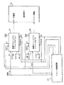
本実施形態に係る表示装置は、コレステリック液晶等のメモリ性の表示材料で構成される単純マトリクス型の表示素子10と、回路に電力を供給する電源21と、電源21の出力電圧を昇圧する昇圧部22と、昇圧部22の出力電圧を複数の電圧値にそれぞれ分岐する多電圧生成部23と、回路にクロックを供給するクロック源24と、複数の制御信号及び画像データを生成するドライバ制御回路25と、スキャンラインを駆動するロウドライバ26(コモンドライバ)と、表示ラインを駆動するカラムドライバ27(セグメントドライバ)と、を備えて構成される。
表示素子10は、例えば、A4判XGA仕様で、1024×768画素を有するものであってよい。電源21は、例えば3V〜5Vの電圧を出力するものでよい。昇圧部22は、DC−DCコンバータなどのレギュレータにより、電源21からの入力電圧を36V〜40Vに昇圧するものである。多電圧生成部23は、昇圧された電圧からロウドライバ(コモンドライバ)26及びカラムドライバ(セグメントドライバ)27に供給する複数の電圧を生成する。
スキャンシフト信号LP_COMはロウドライバ26において表示ラインの更新を指示する信号である。
同図に示すように、制御信号LP_COM及び制御信号LP_SEGを液晶に印加して表示ラインを更新した後、データ取り込みクロックXCLKに応じて1ライン分のデータをカラムドライバ27に供給し、1024個の画素データをシフトして1ライン分の画素データが揃った時点で再び液晶に制御信号LP_COM及び制御信号LP_SEGを印加すると、ロウドライバ26は1スキャンラインに、正極フェーズの電圧パルスを出力する。また、カラムドライバ27は、1024本のデータラインに、1ライン分の画像データに対応した正極フェーズの電圧パルスを出力する。
以下、同様の処理を繰り返して、全画面に表示データに応じた正極及び負極フェーズの電圧パルスの印加を行う。階調レベルに対応したパルスの累積印加時間を、液晶に印加する電圧パルスのパルス数で調整する場合は、各データライン毎に印加する電圧パルスの回数を変化させ、パルス長で調整する場合は、各データライン毎に液晶に印加する電圧パルスのパルス幅を変化させる。
図10Aは、図9のモード選択機能付き単純マトリクスドライバICのセグメントモード時の入力信号と出力電圧の関係を示す説明図である。
図10Bは、図9のモード選択機能付き単純マトリクスドライバICのコモンモード時の入力信号と出力電圧の関係を示す説明図である。
同図に示すように、コモンモード時のドライバは、表示装置駆動信号/DSPOFが「高(HIGH:1)」の時にデータラッチ信号に応じた出力を行い、/DSPOFが「低(LOW:0)」の時には出力は所定値V5(例えばGND)になる。データ信号が"1"で、極性制御信号FRが"1"の時にはV5(GND)を出力し、極性制御信号FRが"0"の時にはV0(20V)を出力し、データ信号が"0"で、極性制御信号FRが"1"の時にはV21(15V)を、極性制御信号FR"0"の時にはV34(5V)を出力する。V0、V21、V34は、外部からドライバに供給される電圧であり、V0≧V21≧V34≧GNDの制限条件を満たす必要がある。
同図において、パルス信号XCLKはデータの取り込み用のクロックを示す(図6,12参照)。また、パルス信号LPはデータ確定用のラッチパルスを示し、ラインデータ転送時に立ち上がる切替え信号S/Cはセグメントモードとコモンモードとの切替えを指示する制御信号を示し、周期的な立ち上がりと立ち下がりとを反復するフレーム信号FRは印加電圧の極性を反転させて液晶に特有の経時劣化を回復させるパルス極性制御信号を示し、表示装置駆動信号/DSPOF(DSPOFバー、図6に示す/DSPOFと同じ信号)は液晶表示装置の駆動信号であり、より具体的には印加電圧の強制オフ信号(印加電圧をオフにする信号、即ち信号DSPOF)の反転信号を示している(図12参照)。さらに、OUT電圧は、ラインデータを表示(表示)させるために液晶に印加する電圧である。
同図に示すように、本実施形態に係る表示装置の単純マトリクスドライバは、データ転送期間において、図13に示す表示装置駆動信号/DSPOF(DSPOFバー)を立ち下げ、その後に、切替え信号S/Cを切替えて立ち上げ、セグメントモード側にする。また、これと同時に、データの取り込み用のクロックとしてパルス信号XCLKを出力し、表示データであるDataを出力する。これらの出力が完了すると、パルス信号LPがデータ確定用のラッチパルスを出力して表示データ(Data)の取り込みがなされ、最後に、ラインデータを出力(表示)させるためのOUT電圧(図13)が液晶に印加されて、データが表示される。
同図において、制御部100は、本実施形態に係る表示装置が備えるドライバ制御回路25の機能ブロックである。
CLK(クロック)生成部101は、外部入力によって周期の設定が可能なパルス信号CLK(図13)を生成する。また、分周部102は、CLK(クロック)生成部101からのクロックを受けて、シーケンス制御に必要なクロックに分周する。分周部102が出力するクロックはシーケンス制御に必要な制御信号の生成タイミングを出力するカウンタ109に送出される。
Claims (4)
- マトリクス型の表示素子と、前記表示素子のスキャン電極を駆動するロウドライバと、前記表示素子のデータ電極を駆動するカラムドライバと、を備える表示装置であって、
データ取り込み用のクロックであるパルス信号XCLK、データ確定用のラッチパルスであるパルス信号LP、液晶の劣化を防止するためのパルス極性制御信号であるフレーム信号FR、及び表示装置駆動停止期間を指示する/DSPOF信号、から成る制御信号を前記ロウドライバ及び前記カラムドライバにそれぞれ出力する手段と、
前記パルス信号XCLKにしたがって前記制御信号を出力する手段から前記カラムドライバに表示データの転送を行うことが可能なセグメントモードであるか、それとも前記パルス信号LPに応じて、前記カラムドライバが前記転送された表示データを前記表示素子へと出力を行うコモンモードであるかの、いずれか1つのモードを指定する切替え信号S/Cを前記ロウドライバ及び前記カラムドライバに出力する手段と、
前記フレーム信号FRの立ち下がり時に生じる液晶への突入電流を防止するために前記/DSPOF信号によって設定される、前記ロウドライバ及び前記カラムドライバから前記表示素子への出力が停止される表示装置駆動停止期間については、表示データの転送が可能な前記セグメントモードにする手段と、
前記セグメントモードに切替えられた前記表示装置駆動停止期間に、前記制御信号を出力する手段から前記カラムドライバに前記表示データの一部を転送する手段と、
を備えたことを特徴とする表示装置。 - 前記セグメントモードに切替えられた期間に転送される前記表示データの一部は、1ライン分の表示データのうちの前半分のデータであることを特徴とする請求項1記載の表示装置。
- 前記制御信号及び切替え信号S/Cは、フルカラー表示が可能な液晶表示パネルの前記ロウドライバ及びカラムドライバに入力され、前記表示データの出力信号は、前記フルカラー表示が可能な液晶表示パネルに入力されることを特徴とする請求項1または請求項2に記載の表示装置。
- 前記フルカラー表示が可能な液晶表示パネルは、赤、緑、青、の光色にそれぞれ対応した3層の液晶表示パネルで構成されていることを特徴とする請求項3記載の表示装置。
Applications Claiming Priority (1)
| Application Number | Priority Date | Filing Date | Title |
|---|---|---|---|
| PCT/JP2007/001500 WO2009084075A1 (ja) | 2007-12-28 | 2007-12-28 | 単純マトリクス型の表示素子を有する表示装置 |
Publications (2)
| Publication Number | Publication Date |
|---|---|
| JPWO2009084075A1 JPWO2009084075A1 (ja) | 2011-05-12 |
| JP5065417B2 true JP5065417B2 (ja) | 2012-10-31 |
Family
ID=40823815
Family Applications (1)
| Application Number | Title | Priority Date | Filing Date |
|---|---|---|---|
| JP2009547818A Active JP5065417B2 (ja) | 2007-12-28 | 2007-12-28 | 単純マトリクス型の表示素子を有する表示装置 |
Country Status (3)
| Country | Link |
|---|---|
| US (1) | US8330751B2 (ja) |
| JP (1) | JP5065417B2 (ja) |
| WO (1) | WO2009084075A1 (ja) |
Families Citing this family (2)
| Publication number | Priority date | Publication date | Assignee | Title |
|---|---|---|---|---|
| CN116256910A (zh) * | 2021-12-09 | 2023-06-13 | 虹彩光电股份有限公司 | 胆固醇液晶显示器装置及清除画面时降低涌浪电流的控制方法 |
| CN116953969A (zh) * | 2022-04-18 | 2023-10-27 | 虹彩光电股份有限公司 | 复合时序模式的胆固醇液晶显示器、液晶驱动单元、以及驱动方法 |
Citations (3)
| Publication number | Priority date | Publication date | Assignee | Title |
|---|---|---|---|---|
| JPH01213695A (ja) * | 1988-02-20 | 1989-08-28 | Fujitsu General Ltd | マトリックス型表示パネルの駆動回路 |
| JPH07159755A (ja) * | 1993-12-07 | 1995-06-23 | Casio Comput Co Ltd | 光源装置及びカラー液晶表示装置 |
| JP2007304527A (ja) * | 2006-05-15 | 2007-11-22 | Fujitsu Frontech Ltd | メモリ性液晶のリセット方法及び液晶表示装置 |
Family Cites Families (11)
| Publication number | Priority date | Publication date | Assignee | Title |
|---|---|---|---|---|
| JPH02212886A (ja) | 1989-02-14 | 1990-08-24 | Seiko Epson Corp | 液晶駆動回路 |
| JPH0462516A (ja) | 1990-06-30 | 1992-02-27 | Toshiba Lighting & Technol Corp | 液晶表示装置 |
| KR0140041B1 (ko) * | 1993-02-09 | 1998-06-15 | 쯔지 하루오 | 표시 장치용 전압 발생 회로, 공통 전극 구동 회로, 신호선 구동 회로 및 계조 전압 발생 회로 |
| CN1162736C (zh) * | 1995-12-14 | 2004-08-18 | 精工爱普生株式会社 | 显示装置的驱动方法、显示装置及电子装置 |
| JPH1138941A (ja) | 1997-07-22 | 1999-02-12 | Nec Ic Microcomput Syst Ltd | 液晶表示回路 |
| JP2000147466A (ja) | 1998-11-17 | 2000-05-26 | Minolta Co Ltd | 液晶表示素子の駆動方法及び情報表示装置 |
| JP2000171837A (ja) | 1998-12-01 | 2000-06-23 | Minolta Co Ltd | 液晶表示素子の駆動方法及び情報表示装置 |
| JP4154828B2 (ja) | 2000-02-17 | 2008-09-24 | コニカミノルタホールディングス株式会社 | 液晶表示素子の駆動方法及び液晶表示装置 |
| US6950086B2 (en) * | 2000-04-03 | 2005-09-27 | Optrex Corporation | Driving method for a cholesteric liquid crystal display device having a memory mode of operation and a driving apparatus |
| US6961036B2 (en) * | 2003-01-29 | 2005-11-01 | Himax Technologies, Inc. | Single polar driving method for cholesteric liquid crystal displays |
| JP4998560B2 (ja) * | 2007-11-21 | 2012-08-15 | 富士通株式会社 | 液晶表示素子及びその駆動方法 |
-
2007
- 2007-12-28 JP JP2009547818A patent/JP5065417B2/ja active Active
- 2007-12-28 WO PCT/JP2007/001500 patent/WO2009084075A1/ja not_active Ceased
-
2010
- 2010-01-05 US US12/652,501 patent/US8330751B2/en active Active
Patent Citations (3)
| Publication number | Priority date | Publication date | Assignee | Title |
|---|---|---|---|---|
| JPH01213695A (ja) * | 1988-02-20 | 1989-08-28 | Fujitsu General Ltd | マトリックス型表示パネルの駆動回路 |
| JPH07159755A (ja) * | 1993-12-07 | 1995-06-23 | Casio Comput Co Ltd | 光源装置及びカラー液晶表示装置 |
| JP2007304527A (ja) * | 2006-05-15 | 2007-11-22 | Fujitsu Frontech Ltd | メモリ性液晶のリセット方法及び液晶表示装置 |
Also Published As
| Publication number | Publication date |
|---|---|
| WO2009084075A1 (ja) | 2009-07-09 |
| JPWO2009084075A1 (ja) | 2011-05-12 |
| US20100103154A1 (en) | 2010-04-29 |
| US8330751B2 (en) | 2012-12-11 |
Similar Documents
| Publication | Publication Date | Title |
|---|---|---|
| CN101828143B (zh) | 具有点阵型显示元件的显示装置及其驱动方法 | |
| JP5163652B2 (ja) | ドットマトリクス型の表示素子を有する表示装置およびその駆動方法 | |
| US20100194793A1 (en) | Cholesteric liquid crystal display device | |
| JPWO2006103738A1 (ja) | 液晶表示素子の駆動方法 | |
| JP5005039B2 (ja) | 単純マトリクス型の表示素子を有する表示装置および単純マトリクスドライバ | |
| JP2012078525A (ja) | 表示装置及びその駆動方法 | |
| JP3807205B2 (ja) | コレステリック液晶表示装置 | |
| JP5065417B2 (ja) | 単純マトリクス型の表示素子を有する表示装置 | |
| JP4668984B2 (ja) | 表示素子の駆動方法 | |
| JP5234829B2 (ja) | 単純マトリクス型の表示素子を有する表示装置 | |
| JP4992969B2 (ja) | 表示装置の駆動方法及び表示装置 | |
| JP2004013121A (ja) | 液晶表示装置の駆動方法 | |
| JP5115217B2 (ja) | ドットマトリクス型液晶表示装置 | |
| CN101981495B (zh) | 胆甾型液晶面板的多灰度驱动电路、驱动方法及显示装置 | |
| JP2009181106A (ja) | ドットマトリクス型表示装置および画像書込み方法 | |
| JP5332339B2 (ja) | 表示装置 | |
| JP2013205673A (ja) | コレステリック液晶の表示装置及びその表示方法 | |
| JP2012003017A (ja) | 表示装置 | |
| JP2009163092A (ja) | 液晶表示素子の駆動方法および液晶表示装置 | |
| JP2010102160A (ja) | 液晶表示装置 | |
| JP5310517B2 (ja) | 液晶駆動方法 | |
| JP5272487B2 (ja) | ドットマトリクス型の表示装置 | |
| JP2010145975A (ja) | 表示素子の駆動方法及び表示装置 | |
| JP2009204932A (ja) | ドットマトリクス型表示装置 |
Legal Events
| Date | Code | Title | Description |
|---|---|---|---|
| A131 | Notification of reasons for refusal |
Free format text: JAPANESE INTERMEDIATE CODE: A131 Effective date: 20120221 |
|
| A521 | Request for written amendment filed |
Free format text: JAPANESE INTERMEDIATE CODE: A523 Effective date: 20120420 |
|
| A131 | Notification of reasons for refusal |
Free format text: JAPANESE INTERMEDIATE CODE: A131 Effective date: 20120522 |
|
| A521 | Request for written amendment filed |
Free format text: JAPANESE INTERMEDIATE CODE: A523 Effective date: 20120717 |
|
| TRDD | Decision of grant or rejection written | ||
| A01 | Written decision to grant a patent or to grant a registration (utility model) |
Free format text: JAPANESE INTERMEDIATE CODE: A01 Effective date: 20120807 |
|
| A01 | Written decision to grant a patent or to grant a registration (utility model) |
Free format text: JAPANESE INTERMEDIATE CODE: A01 |
|
| A61 | First payment of annual fees (during grant procedure) |
Free format text: JAPANESE INTERMEDIATE CODE: A61 Effective date: 20120809 |
|
| R150 | Certificate of patent or registration of utility model |
Ref document number: 5065417 Country of ref document: JP Free format text: JAPANESE INTERMEDIATE CODE: R150 Free format text: JAPANESE INTERMEDIATE CODE: R150 |
|
| FPAY | Renewal fee payment (event date is renewal date of database) |
Free format text: PAYMENT UNTIL: 20150817 Year of fee payment: 3 |
|
| R250 | Receipt of annual fees |
Free format text: JAPANESE INTERMEDIATE CODE: R250 |
|
| R250 | Receipt of annual fees |
Free format text: JAPANESE INTERMEDIATE CODE: R250 |
|
| S111 | Request for change of ownership or part of ownership |
Free format text: JAPANESE INTERMEDIATE CODE: R313113 |
|
| R350 | Written notification of registration of transfer |
Free format text: JAPANESE INTERMEDIATE CODE: R350 |
|
| RD02 | Notification of acceptance of power of attorney |
Free format text: JAPANESE INTERMEDIATE CODE: R3D02 |
|
| R250 | Receipt of annual fees |
Free format text: JAPANESE INTERMEDIATE CODE: R250 |
|
| R250 | Receipt of annual fees |
Free format text: JAPANESE INTERMEDIATE CODE: R250 |
|
| R250 | Receipt of annual fees |
Free format text: JAPANESE INTERMEDIATE CODE: R250 |
|
| R250 | Receipt of annual fees |
Free format text: JAPANESE INTERMEDIATE CODE: R250 |
|
| R250 | Receipt of annual fees |
Free format text: JAPANESE INTERMEDIATE CODE: R250 |
|
| R250 | Receipt of annual fees |
Free format text: JAPANESE INTERMEDIATE CODE: R250 |
|
| R250 | Receipt of annual fees |
Free format text: JAPANESE INTERMEDIATE CODE: R250 |
|
| R250 | Receipt of annual fees |
Free format text: JAPANESE INTERMEDIATE CODE: R250 |
|
| R250 | Receipt of annual fees |
Free format text: JAPANESE INTERMEDIATE CODE: R250 |