JP5114069B2 - 電子モジュールおよび電子モジュールをカプセル化する方法 - Google Patents
電子モジュールおよび電子モジュールをカプセル化する方法 Download PDFInfo
- Publication number
- JP5114069B2 JP5114069B2 JP2007043887A JP2007043887A JP5114069B2 JP 5114069 B2 JP5114069 B2 JP 5114069B2 JP 2007043887 A JP2007043887 A JP 2007043887A JP 2007043887 A JP2007043887 A JP 2007043887A JP 5114069 B2 JP5114069 B2 JP 5114069B2
- Authority
- JP
- Japan
- Prior art keywords
- film
- module
- housing body
- module according
- optoelectronic component
- Prior art date
- Legal status (The legal status is an assumption and is not a legal conclusion. Google has not performed a legal analysis and makes no representation as to the accuracy of the status listed.)
- Active
Links
Images
Classifications
-
- H—ELECTRICITY
- H10—SEMICONDUCTOR DEVICES; ELECTRIC SOLID-STATE DEVICES NOT OTHERWISE PROVIDED FOR
- H10H—INORGANIC LIGHT-EMITTING SEMICONDUCTOR DEVICES HAVING POTENTIAL BARRIERS
- H10H20/00—Individual inorganic light-emitting semiconductor devices having potential barriers, e.g. light-emitting diodes [LED]
- H10H20/80—Constructional details
- H10H20/85—Packages
- H10H20/8506—Containers
-
- H—ELECTRICITY
- H10—SEMICONDUCTOR DEVICES; ELECTRIC SOLID-STATE DEVICES NOT OTHERWISE PROVIDED FOR
- H10F—INORGANIC SEMICONDUCTOR DEVICES SENSITIVE TO INFRARED RADIATION, LIGHT, ELECTROMAGNETIC RADIATION OF SHORTER WAVELENGTH OR CORPUSCULAR RADIATION
- H10F77/00—Constructional details of devices covered by this subclass
- H10F77/50—Encapsulations or containers
-
- H—ELECTRICITY
- H10—SEMICONDUCTOR DEVICES; ELECTRIC SOLID-STATE DEVICES NOT OTHERWISE PROVIDED FOR
- H10H—INORGANIC LIGHT-EMITTING SEMICONDUCTOR DEVICES HAVING POTENTIAL BARRIERS
- H10H20/00—Individual inorganic light-emitting semiconductor devices having potential barriers, e.g. light-emitting diodes [LED]
- H10H20/80—Constructional details
- H10H20/85—Packages
- H10H20/855—Optical field-shaping means, e.g. lenses
Landscapes
- Led Device Packages (AREA)
- Semiconductor Lasers (AREA)
- Light Receiving Elements (AREA)
- Optical Integrated Circuits (AREA)
Description
A)内部にオプトエレクトロニクス構成素子が配置される凹部を備えたハウジングボディを有する電子モジュールを準備するステップ
B)ポリイミドを有するフィルムを空洞部が形成されるように凹部上に被着するステップ。
A1)ポリイミドを有するフィルム帯材を準備するステップ
A2)切断および/または打抜きによりフィルム帯材からフィルムを分離するステップ。
Claims (28)
- 電子モジュールにおいて
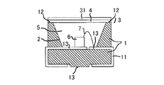
−オプトエレクトロニクス構成素子(6)が配置される凹部(2)を有するハウジングボディ(1)と、
−空洞部(5)が形成されるように前記凹部(2)上に配置されている、ポリイミドを有するフィルム(3)とを包含し、
前記フィルム(3)は、接着層(4)を用いて前記ハウジングボディ(1)上に被着されており、且つ、前記接着層(4)は前記空洞部を気密に閉じずに、周囲に関する該空洞部内の圧力の補償調整を実現する厚さを有することを特徴とする、モジュール。 - 前記ハウジングボディは、前記空洞部を包囲する平坦な表面を有し、該表面上には前記接着層が配置されており、それにより前記凹部を包囲する前記フィルムの領域が前記ハウジングボディに被着されている、請求項1記載のモジュール。
- 前記オプトエレクトロニクス構成素子は前記フィルムと機械的に直接接触しない、請求項1または2記載のモジュール。
- 前記フィルムは複屈折性である、請求項1から3までのいずれか1項記載のモジュール。
- 前記フィルム(3)は、前記ポリイミドを包含する少なくとも1つの第1の層(31)と第2の層とを有し、前記第2の層は接着層(4)を有し、且つ前記ハウジングボディ(1)上に配置されている、請求項1から4までのいずれか1項記載のモジュール。
- 前記接着層(4)はシリコーン接着剤を有する、請求項1から5までのいずれか1項記載のモジュール。
- 前記フィルム(3)または該フィルム(3)の前記第1の層(31)はポリイミドである、請求項1から6までのいずれか1項記載のモジュール。
- 前記ポリイミドはポリ−(酸化ジフェニル−ピロメリトイミド)である、請求項1から7までのいずれか1項記載のモジュール。
- 前記フィルム(3)は70μmの厚さを有する、請求項1から8までのいずれか1項記載のモジュール。
- 前記フィルム(3)はモジュールの動作時に前記ハウジングボディ(1)上に残存する、請求項1から9までのいずれか1項記載のモジュール。
- 前記フィルム(3)は前記オプトエレクトロニクス構成素子のビーム路内に配置されている、請求項1から10までのいずれか1項記載のモジュール。
- 前記フィルム(3)はビームに対して透過性である、請求項1から11までのいずれか1項記載のモジュール。
- 前記フィルム(3)は800nm〜900nmの波長領域においてビームに対して透過性である、請求項12記載のモジュール。
- 前記フィルム(3)の透過性は、−40℃〜100℃の温度領域においては温度に依存しない、請求項12または13記載のモジュール。
- 前記フィルム(3)は静電防止性である、請求項1から14までのいずれか1項記載のモジュール。
- 前記オプトエレクトロニクス構成素子(6)はビーム検出型のオプトエレクトロニクス構成素子またはビーム放射型のオプトエレクトロニクス構成素子である、請求項1から15までのいずれか1項記載のモジュール。
- 前記ビーム検出型のオプトエレクトロニクス構成素子はフォトダイオード、フォトトランジスタまたはフォトICである、請求項16記載のモジュール。
- 前記ビーム放射型のオプトエレクトロニクス構成素子はビーム放射型の半導体ダイオードまたは半導体レーザダイオードである、請求項16記載のモジュール。
- 前記半導体レーザダイオードは面放射型レーザダイオード(VCSEL)である、請求項18記載のモジュール。
- 前記ハウジングボディ(1)は表面実装可能なものである、請求項1から19までのいずれか1項記載のモジュール。
- 前記ハウジングボディ(1)はプラスチックからなる、請求項1から20までのいずれか1項記載のモジュール。
- 請求項1から21までのいずれか1項記載の電子モジュールをカプセル化する方法において、
A)オプトエレクトロニクス構成素子(6)が配置される凹部(2)を備えたハウジングボディ(1)を有する前記電子モジュールを準備するステップと、
B)空洞部(5)が形成されるように、ポリイミドを有するフィルム(3)を前記凹部(2)上に被着するステップとを有し、ただし、前記フィルム(3)を接着層(4)を用いて前記ハウジングボディ(1)上に被着し、前記接着層(4)は、前記空洞部を気密に閉じずに、周囲に関する該空洞部内の圧力の補償調整を実現する厚さを有することを特徴とする、電子モジュールをカプセル化する方法。 - 前記ステップB)の前に、
A1)ポリイミドを有するフィルム帯材を準備するステップと、
A2)切断および/または打抜きにより前記フィルム帯材から前記フィルム(3)を分離するステップとを有する、請求項22記載の方法。 - 前記ステップB)は、
B1)前記フィルム(3)を真空ピペットを用いて取り上げるステップと、
B2)前記フィルム(3)を真空ピペットを用いて前記凹部(2)上に載着するステップとを有する、請求項22または23記載の方法。 - 前記ハウジングボディ(1)を、前記フィルム(3)の載着後にさらに基板に載着する、請求項22から24までのいずれか1項記載の方法。
- 前記基板は回路基板を包含する、請求項25記載の方法。
- 前記ハウジングボディを溶接はんだ法を用いて前記基板上に被着する、請求項25または26記載の方法。
- 前記フィルム(3)をモジュールの使用開始前に前記ハウジングボディ(1)から除去する、請求項22から27までのいずれか1項記載の方法。
Applications Claiming Priority (2)
| Application Number | Priority Date | Filing Date | Title |
|---|---|---|---|
| DE102006008793A DE102006008793A1 (de) | 2006-02-24 | 2006-02-24 | Elektronisches Bauteil |
| DE102006008793.3 | 2006-02-24 |
Publications (2)
| Publication Number | Publication Date |
|---|---|
| JP2007227935A JP2007227935A (ja) | 2007-09-06 |
| JP5114069B2 true JP5114069B2 (ja) | 2013-01-09 |
Family
ID=38048419
Family Applications (1)
| Application Number | Title | Priority Date | Filing Date |
|---|---|---|---|
| JP2007043887A Active JP5114069B2 (ja) | 2006-02-24 | 2007-02-23 | 電子モジュールおよび電子モジュールをカプセル化する方法 |
Country Status (4)
| Country | Link |
|---|---|
| US (1) | US7851812B2 (ja) |
| EP (1) | EP1826832A3 (ja) |
| JP (1) | JP5114069B2 (ja) |
| DE (1) | DE102006008793A1 (ja) |
Families Citing this family (12)
| Publication number | Priority date | Publication date | Assignee | Title |
|---|---|---|---|---|
| TWI342536B (en) * | 2006-09-11 | 2011-05-21 | Au Optronics Corp | Signal regulator module and related display device |
| TW201020643A (en) * | 2008-11-25 | 2010-06-01 | Chi Mei Lighting Tech Corp | Side view type light-emitting diode package structure, and manufacturing method and application thereof |
| TWI380483B (en) * | 2008-12-29 | 2012-12-21 | Everlight Electronics Co Ltd | Led device and method of packaging the same |
| DE102009004724A1 (de) * | 2009-01-15 | 2010-07-22 | Osram Opto Semiconductors Gmbh | Verfahren zur Herstellung eines optoelektronischen Bauteils und optoelektronisches Bauteil |
| TWM379163U (en) * | 2009-11-26 | 2010-04-21 | Truelight Corp | Packaging apparatus for high power and high orientation matrix semiconductor light-emitting devices |
| CN102544338A (zh) * | 2010-12-10 | 2012-07-04 | 富士康(昆山)电脑接插件有限公司 | 发光二极管导线架 |
| DE112011105262B4 (de) | 2011-05-19 | 2025-10-16 | OSRAM Opto Semiconductors Gesellschaft mit beschränkter Haftung | Optoelektronische Vorrichtung und Verfahren zur Herstellung von optoelektronischen Vorrichtungen |
| WO2013036481A2 (en) * | 2011-09-06 | 2013-03-14 | Cree, Inc. | Light emitter packages and devices having improved wire bonding and related methods |
| KR101371258B1 (ko) * | 2012-05-15 | 2014-03-07 | 주식회사 나무가 | 레이저 다이오드 패키지 및 상기 레이저 다이오드 패키지를 사용하는 3D Depth 카메라 |
| DE102012107794B4 (de) * | 2012-08-23 | 2023-10-19 | OSRAM Opto Semiconductors Gesellschaft mit beschränkter Haftung | Optoelektronische Vorrichtung |
| CN111917001B (zh) * | 2019-05-07 | 2021-07-23 | 光宝光电(常州)有限公司 | 光源装置 |
| DE102021119709A1 (de) * | 2021-07-29 | 2023-02-02 | OSRAM Opto Semiconductors Gesellschaft mit beschränkter Haftung | Anordnung, verfahren zur montage eines optoelektronischen bauteils und optoelektronisches bauteil |
Family Cites Families (38)
| Publication number | Priority date | Publication date | Assignee | Title |
|---|---|---|---|---|
| JPS5353983U (ja) * | 1976-10-12 | 1978-05-09 | ||
| JPS5936837B2 (ja) * | 1977-04-05 | 1984-09-06 | 株式会社東芝 | 光半導体装置 |
| US4975762A (en) * | 1981-06-11 | 1990-12-04 | General Electric Ceramics, Inc. | Alpha-particle-emitting ceramic composite cover |
| DE3337195A1 (de) * | 1983-10-13 | 1985-04-25 | Telefunken electronic GmbH, 7100 Heilbronn | Anordnung fuer ein bei niederen temperaturen betriebsfaehiges elektronisches bauelement |
| US4926545A (en) * | 1989-05-17 | 1990-05-22 | At&T Bell Laboratories | Method of manufacturing optical assemblies |
| US5117279A (en) * | 1990-03-23 | 1992-05-26 | Motorola, Inc. | Semiconductor device having a low temperature uv-cured epoxy seal |
| DE19536454B4 (de) | 1995-09-29 | 2006-03-09 | Osram Opto Semiconductors Gmbh | Optoelektronisches Halbleiter-Bauelement |
| DE19549818B4 (de) * | 1995-09-29 | 2010-03-18 | Osram Opto Semiconductors Gmbh | Optoelektronisches Halbleiter-Bauelement |
| US6583444B2 (en) * | 1997-02-18 | 2003-06-24 | Tessera, Inc. | Semiconductor packages having light-sensitive chips |
| DE19751911A1 (de) * | 1997-11-22 | 1999-06-02 | Vishay Semiconductor Gmbh | Leuchtdiode mit einem hermetisch dichten Gehäuse und Verfahren zu deren Herstellung |
| US6054008A (en) * | 1998-01-22 | 2000-04-25 | International Business Machines Corporation | Process for adhesively attaching a temporary lid to a microelectronic package |
| DE19845229C1 (de) * | 1998-10-01 | 2000-03-09 | Wustlich Daniel | Mit Weißlicht arbeitende Hintergrundbeleuchtung |
| DE19945134C2 (de) | 1999-09-21 | 2003-08-14 | Osram Opto Semiconductors Gmbh | Lichtemittierendes Halbleiterbauelement hoher ESD-Festigkeit und Verfahren zu seiner Herstellung |
| FR2800911B1 (fr) * | 1999-11-04 | 2003-08-22 | St Microelectronics Sa | Boitier semi-conducteur optique et procede de fabrication d'un tel boitier |
| TW572925B (en) * | 2000-01-24 | 2004-01-21 | Mitsui Chemicals Inc | Urethane resin composition for sealing optoelectric conversion devices |
| DE10026262B4 (de) * | 2000-05-26 | 2005-03-17 | Osram Opto Semiconductors Gmbh | Vertikalresonator-Laserdiode (VCSEL) |
| JP2001345482A (ja) * | 2000-06-01 | 2001-12-14 | Toshiba Corp | 蛍光表示装置 |
| DE10038235A1 (de) | 2000-08-04 | 2002-02-21 | Osram Opto Semiconductors Gmbh | Oberflächenemittierender Laser mit seitlicher Strominjektion |
| DE10041328B4 (de) * | 2000-08-23 | 2018-04-05 | Osram Opto Semiconductors Gmbh | Verpackungseinheit für Halbleiterchips |
| US6759266B1 (en) * | 2001-09-04 | 2004-07-06 | Amkor Technology, Inc. | Quick sealing glass-lidded package fabrication method |
| JP2003188406A (ja) * | 2001-12-20 | 2003-07-04 | Sumitomo Electric Ind Ltd | 受光素子、これを用いた光受信器および製造方法 |
| TWI226357B (en) * | 2002-05-06 | 2005-01-11 | Osram Opto Semiconductors Gmbh | Wavelength-converting reaction-resin, its production method, light-radiating optical component and light-radiating semiconductor-body |
| WO2003093393A1 (de) * | 2002-05-06 | 2003-11-13 | Osram Opto Semiconductors Gmbh | Wellenlängenkonvertierende reaktionsharzmasse und leuchtdiodenbauelement |
| JP3962282B2 (ja) * | 2002-05-23 | 2007-08-22 | 松下電器産業株式会社 | 半導体装置の製造方法 |
| US7479662B2 (en) * | 2002-08-30 | 2009-01-20 | Lumination Llc | Coated LED with improved efficiency |
| US7078737B2 (en) * | 2002-09-02 | 2006-07-18 | Matsushita Electric Industrial Co., Ltd. | Light-emitting device |
| JP3782411B2 (ja) * | 2002-09-02 | 2006-06-07 | 松下電器産業株式会社 | 発光装置 |
| KR20050103200A (ko) * | 2003-01-27 | 2005-10-27 | 쓰리엠 이노베이티브 프로퍼티즈 컴파니 | 인광계 광원 요소와 제조 방법 |
| EP1687879B1 (de) | 2003-11-28 | 2008-12-10 | OSRAM Opto Semiconductors GmbH | Lichtemittierendes halbleiterbauelement mit einer schutzdiode |
| DE102004005269B4 (de) | 2003-11-28 | 2005-09-29 | Osram Opto Semiconductors Gmbh | Lichtemittierendes Halbleiterbauelement mit einer Schutzdiode |
| JP4116607B2 (ja) * | 2004-04-28 | 2008-07-09 | 日東電工株式会社 | 映像センサの実装方法およびそれに用いる粘着テープ |
| US6881980B1 (en) * | 2004-06-17 | 2005-04-19 | Chunghwa Picture Tubes, Ltd. | Package structure of light emitting diode |
| US7745832B2 (en) * | 2004-09-24 | 2010-06-29 | Epistar Corporation | Semiconductor light-emitting element assembly with a composite substrate |
| DE102004063133A1 (de) * | 2004-12-22 | 2006-07-13 | Schott Ag | Organisches elektrisches oder elektronisches Bauelement mit erhöhter Lebensdauer |
| JP4945106B2 (ja) * | 2005-09-08 | 2012-06-06 | スタンレー電気株式会社 | 半導体発光装置 |
| US20070190747A1 (en) * | 2006-01-23 | 2007-08-16 | Tessera Technologies Hungary Kft. | Wafer level packaging to lidded chips |
| US8212271B2 (en) * | 2007-10-11 | 2012-07-03 | Hitachi Chemical Co., Ltd. | Substrate for mounting an optical semiconductor element, manufacturing method thereof, an optical semiconductor device, and manufacturing method thereof |
| US7915802B2 (en) * | 2007-11-12 | 2011-03-29 | Rohm Co., Ltd. | Surface light emitting device and polarization light source |
-
2006
- 2006-02-24 DE DE102006008793A patent/DE102006008793A1/de not_active Ceased
-
2007
- 2007-02-15 EP EP07003234.7A patent/EP1826832A3/de not_active Ceased
- 2007-02-23 US US11/678,523 patent/US7851812B2/en active Active
- 2007-02-23 JP JP2007043887A patent/JP5114069B2/ja active Active
Also Published As
| Publication number | Publication date |
|---|---|
| EP1826832A3 (de) | 2013-09-25 |
| US20070200130A1 (en) | 2007-08-30 |
| DE102006008793A1 (de) | 2007-09-13 |
| US7851812B2 (en) | 2010-12-14 |
| JP2007227935A (ja) | 2007-09-06 |
| EP1826832A2 (de) | 2007-08-29 |
Similar Documents
| Publication | Publication Date | Title |
|---|---|---|
| JP5114069B2 (ja) | 電子モジュールおよび電子モジュールをカプセル化する方法 | |
| CN103548148B (zh) | 光电子装置和用于制造光电子装置的方法 | |
| US7246953B2 (en) | Optical device package | |
| US8159595B2 (en) | Camera module having circuit component | |
| US7521770B2 (en) | Image capturing device | |
| CN102388469B (zh) | 紧密光电构件封装物的制造 | |
| CN101569023A (zh) | 用于光电子器件的壳体和光电子器件在壳体中的布置 | |
| US20190067901A1 (en) | Integrated package for laser driver and laser diode | |
| JP5375219B2 (ja) | 撮像装置 | |
| JP5610156B2 (ja) | 光電変換モジュール及び光電変換モジュールの製造方法 | |
| CN103858230A (zh) | 光电子模块和用于制造该光电子模块的方法 | |
| US10510932B2 (en) | Optoelectronic modules including optoelectronic device subassemblies and methods of manufacturing the same | |
| JP6324442B2 (ja) | 電子モジュールおよび光電デバイス | |
| WO2012005852A2 (en) | Vent structures for encapsulated components on an soi-based photonics platform | |
| US6827503B2 (en) | Optical device package having a configured frame | |
| US20090278157A1 (en) | Method for the production of a semiconductor component comprising a planar contact, and semiconductor component | |
| JP5639271B2 (ja) | オプトエレクトロニクス半導体部品の製造方法 | |
| CN1649163A (zh) | 固体摄像装置用半导体元件和采用该元件的固体摄像装置 | |
| CN107818999B (zh) | 半导体装置的制造方法以及半导体装置 | |
| JP2010273087A (ja) | 半導体装置及びその製造方法 | |
| JPH0846224A (ja) | オプトエレクトロニック組立体及びその製造方法及び使用方法 | |
| KR20210115480A (ko) | 이미지 센서 패키지 및 이를 포함하는 카메라 장치 | |
| JP2007027559A (ja) | 表面実装型電子部品、その製造方法および光学電子機器 | |
| EP1611468B1 (en) | Package for optoelectronic device on wafer level | |
| WO2022043402A1 (en) | Optical device |
Legal Events
| Date | Code | Title | Description |
|---|---|---|---|
| A621 | Written request for application examination |
Free format text: JAPANESE INTERMEDIATE CODE: A621 Effective date: 20091029 |
|
| RD04 | Notification of resignation of power of attorney |
Free format text: JAPANESE INTERMEDIATE CODE: A7424 Effective date: 20101227 |
|
| RD04 | Notification of resignation of power of attorney |
Free format text: JAPANESE INTERMEDIATE CODE: A7424 Effective date: 20101228 |
|
| A131 | Notification of reasons for refusal |
Free format text: JAPANESE INTERMEDIATE CODE: A131 Effective date: 20120210 |
|
| A521 | Request for written amendment filed |
Free format text: JAPANESE INTERMEDIATE CODE: A523 Effective date: 20120510 |
|
| A131 | Notification of reasons for refusal |
Free format text: JAPANESE INTERMEDIATE CODE: A131 Effective date: 20120530 |
|
| A521 | Request for written amendment filed |
Free format text: JAPANESE INTERMEDIATE CODE: A523 Effective date: 20120829 |
|
| TRDD | Decision of grant or rejection written | ||
| A01 | Written decision to grant a patent or to grant a registration (utility model) |
Free format text: JAPANESE INTERMEDIATE CODE: A01 Effective date: 20120914 |
|
| A01 | Written decision to grant a patent or to grant a registration (utility model) |
Free format text: JAPANESE INTERMEDIATE CODE: A01 |
|
| A61 | First payment of annual fees (during grant procedure) |
Free format text: JAPANESE INTERMEDIATE CODE: A61 Effective date: 20121015 |
|
| FPAY | Renewal fee payment (event date is renewal date of database) |
Free format text: PAYMENT UNTIL: 20151019 Year of fee payment: 3 |
|
| R150 | Certificate of patent or registration of utility model |
Free format text: JAPANESE INTERMEDIATE CODE: R150 Ref document number: 5114069 Country of ref document: JP Free format text: JAPANESE INTERMEDIATE CODE: R150 |
|
| R250 | Receipt of annual fees |
Free format text: JAPANESE INTERMEDIATE CODE: R250 |
|
| R250 | Receipt of annual fees |
Free format text: JAPANESE INTERMEDIATE CODE: R250 |
|
| R250 | Receipt of annual fees |
Free format text: JAPANESE INTERMEDIATE CODE: R250 |
|
| R250 | Receipt of annual fees |
Free format text: JAPANESE INTERMEDIATE CODE: R250 |
|
| R250 | Receipt of annual fees |
Free format text: JAPANESE INTERMEDIATE CODE: R250 |
|
| R250 | Receipt of annual fees |
Free format text: JAPANESE INTERMEDIATE CODE: R250 |
|
| R250 | Receipt of annual fees |
Free format text: JAPANESE INTERMEDIATE CODE: R250 |
|
| R250 | Receipt of annual fees |
Free format text: JAPANESE INTERMEDIATE CODE: R250 |
|
| R250 | Receipt of annual fees |
Free format text: JAPANESE INTERMEDIATE CODE: R250 |
|
| R250 | Receipt of annual fees |
Free format text: JAPANESE INTERMEDIATE CODE: R250 |