JP5116522B2 - スイッチング電源装置 - Google Patents
スイッチング電源装置 Download PDFInfo
- Publication number
- JP5116522B2 JP5116522B2 JP2008066788A JP2008066788A JP5116522B2 JP 5116522 B2 JP5116522 B2 JP 5116522B2 JP 2008066788 A JP2008066788 A JP 2008066788A JP 2008066788 A JP2008066788 A JP 2008066788A JP 5116522 B2 JP5116522 B2 JP 5116522B2
- Authority
- JP
- Japan
- Prior art keywords
- voltage
- input voltage
- input
- power supply
- switching power
- Prior art date
- Legal status (The legal status is an assumption and is not a legal conclusion. Google has not performed a legal analysis and makes no representation as to the accuracy of the status listed.)
- Expired - Fee Related
Links
- 239000004065 semiconductor Substances 0.000 claims description 5
- 230000003247 decreasing effect Effects 0.000 claims description 4
- 230000007423 decrease Effects 0.000 description 7
- 230000033228 biological regulation Effects 0.000 description 4
- 238000010586 diagram Methods 0.000 description 4
- 239000003990 capacitor Substances 0.000 description 1
- 238000000034 method Methods 0.000 description 1
- 238000012986 modification Methods 0.000 description 1
- 230000004048 modification Effects 0.000 description 1
Images


Landscapes
- Dc-Dc Converters (AREA)
Description
これに対して車載機に上述のスイッチング電源装置を適用した場合には、動作電圧の範囲内において常に略一定の出力電圧を容易に作成することができる。
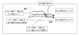
そしてこのトランスを使用する場合、入力電圧が下がったときには、出力電圧も電圧比3:1で低下する。具体的には例えば10Vの入力電圧では出力電圧は30Vとなる。すなわち従来のpush−pull電源装置では、性能に必要な出力電圧をたとえ39Vに設定していても、入力電圧が特定の入力電圧である13Vよりも低い場合には出力電圧のフィードバックが機能しなくなるようになっていた。
一方、出力電圧をフィードバックせずにDuty比を固定することで、入力電圧と出力電圧との間で比例関係を成立させることも可能ではあるが、この場合には出力電圧のレギュレーションを確保できず、出力電圧が大きく変動してしまう虞があった。
3 FET
10 IC
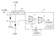
11 エラーAMP
12 コンパレータ
20 ツェナーダイオード
Claims (5)
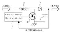
- オン・オフ制御される半導体スイッチにより、直流入力電圧を変換した直流出力電圧を出力する昇圧用のスイッチング出力回路と、
前記直流出力電圧が入力される誤差増幅器と、
前記誤差増幅器の出力信号と三角波信号とを比較して、PWM信号を出力するPWM比較器と、を有するとともに、
前記PWM信号により前記半導体スイッチのオンあるいはオフを制御するスイッチング電源装置であって、
前記誤差増幅器にさらに前記直流入力電圧を入力するとともに、前記誤差増幅器で前記直流出力電圧と前記直流入力電圧とを比較し、
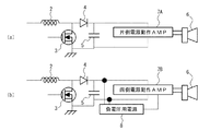
前記直流入力電圧が所定値よりも高い場合に、前記直流入力電圧を所定の電圧に制御するとともに、前記直流入力電圧が所定値以下に低下した場合に、前記直流入力電圧が低下するように前記直流入力電圧を制御する入力電圧制御手段を備えることを特徴とするスイッチング電源装置。 - 前記入力電圧制御手段が、前記直流入力電圧が、前記誤差増幅器に入力される前にツェナーダイオードを介して接地されることで実現される構成であることを特徴とする請求項1記載のスイッチング電源装置。
- 前記入力電圧制御手段が、前記直流入力電圧が、電圧可変レギュレータを介して前記誤差増幅器に入力されることで実現される構成であることを特徴とする請求項1記載のスイッチング電源装置。
- 前記入力電圧制御手段が、さらに前記直流入力電圧が、電子制御装置を介して前記電圧可変レギュレータに入力されることで実現される構成であることを特徴とする請求項3記載のスイッチング電源装置。
- 前記直流入力電圧が、車両が備えるバッテリをメイン電源とする電圧であることを特徴とする請求項1から4のいずれか1項記載のスイッチング電源装置。
Priority Applications (1)
| Application Number | Priority Date | Filing Date | Title |
|---|---|---|---|
| JP2008066788A JP5116522B2 (ja) | 2008-03-14 | 2008-03-14 | スイッチング電源装置 |
Applications Claiming Priority (1)
| Application Number | Priority Date | Filing Date | Title |
|---|---|---|---|
| JP2008066788A JP5116522B2 (ja) | 2008-03-14 | 2008-03-14 | スイッチング電源装置 |
Publications (2)
| Publication Number | Publication Date |
|---|---|
| JP2009225555A JP2009225555A (ja) | 2009-10-01 |
| JP5116522B2 true JP5116522B2 (ja) | 2013-01-09 |
Family
ID=41241747
Family Applications (1)
| Application Number | Title | Priority Date | Filing Date |
|---|---|---|---|
| JP2008066788A Expired - Fee Related JP5116522B2 (ja) | 2008-03-14 | 2008-03-14 | スイッチング電源装置 |
Country Status (1)
| Country | Link |
|---|---|
| JP (1) | JP5116522B2 (ja) |
Family Cites Families (6)
| Publication number | Priority date | Publication date | Assignee | Title |
|---|---|---|---|---|
| JPS60257766A (ja) * | 1984-05-31 | 1985-12-19 | Panafacom Ltd | Dc−dc電力変換器 |
| JP2827188B2 (ja) * | 1992-09-02 | 1998-11-18 | 日本電信電話株式会社 | 電源装置 |
| JP3473509B2 (ja) * | 1999-07-16 | 2003-12-08 | 三菱電機株式会社 | スイッチングレギュレータ |
| JP2002095244A (ja) * | 2000-09-18 | 2002-03-29 | Toshiba Corp | レギュレータ回路 |
| JP3944605B2 (ja) * | 2002-09-30 | 2007-07-11 | ローム株式会社 | スイッチング電源装置 |
| JP4513494B2 (ja) * | 2004-10-15 | 2010-07-28 | トヨタ自動車株式会社 | 電圧変換装置の制御装置及び制御方法 |
-
2008
- 2008-03-14 JP JP2008066788A patent/JP5116522B2/ja not_active Expired - Fee Related
Also Published As
| Publication number | Publication date |
|---|---|
| JP2009225555A (ja) | 2009-10-01 |
Similar Documents
| Publication | Publication Date | Title |
|---|---|---|
| US20180145593A1 (en) | Cycle-by-cycle peak current limiting in crrent mode buck/boost converters | |
| JP2010004653A (ja) | Dc−dcコンバータ | |
| JP5157603B2 (ja) | 昇圧型dc−dcコンバータおよび電源駆動用半導体集積回路 | |
| JP4498851B2 (ja) | 電源装置 | |
| JP4997122B2 (ja) | 電源供給回路及びその動作制御方法 | |
| US8829871B2 (en) | Current mode control for DC-DC converter having peak current dependent variable off-time | |
| JP2017085725A (ja) | 降圧dc/dcコンバータおよびその制御回路、車載用電源装置 | |
| KR20110135803A (ko) | 스위칭 전원장치 | |
| US20100301824A1 (en) | Step-up dc/dc switching converter and semiconductor integrated circuit device | |
| JP2018129907A (ja) | Dc/dcコンバータおよびその制御回路、制御方法、車載電装機器 | |
| US7336057B2 (en) | DC/DC converter | |
| US9385615B2 (en) | Isolated switching power supply | |
| JP5228567B2 (ja) | 昇圧型dc−dcコンバータ | |
| US10135332B2 (en) | DC-DC converter | |
| US10027221B1 (en) | Method of generating a feedback signal in a switching regulator | |
| JP2010158116A (ja) | Dc−dcコンバータ | |
| CN103516218B (zh) | 电源供应装置 | |
| JP5116522B2 (ja) | スイッチング電源装置 | |
| JP6139422B2 (ja) | 基準電圧出力回路および電源装置 | |
| US10811972B2 (en) | Buck-boost converter power supply with drive circuit | |
| JP2006166613A (ja) | スイッチング電源装置 | |
| JP2010098840A (ja) | 昇降圧dc−dcコンバータ | |
| JP2005269838A (ja) | Dc−dcコンバータ | |
| JP2011087389A (ja) | Dc−dcコンバータ及び車両用灯具 | |
| US20080136382A1 (en) | Reference voltage generator for reduced voltage overshoot in a switch mode regulator at the end of soft-start |
Legal Events
| Date | Code | Title | Description |
|---|---|---|---|
| A621 | Written request for application examination |
Free format text: JAPANESE INTERMEDIATE CODE: A621 Effective date: 20101220 |
|
| A521 | Request for written amendment filed |
Free format text: JAPANESE INTERMEDIATE CODE: A523 Effective date: 20120217 |
|
| A131 | Notification of reasons for refusal |
Free format text: JAPANESE INTERMEDIATE CODE: A131 Effective date: 20120807 |
|
| A977 | Report on retrieval |
Free format text: JAPANESE INTERMEDIATE CODE: A971007 Effective date: 20120808 |
|
| A521 | Request for written amendment filed |
Free format text: JAPANESE INTERMEDIATE CODE: A523 Effective date: 20120903 |
|
| TRDD | Decision of grant or rejection written | ||
| A01 | Written decision to grant a patent or to grant a registration (utility model) |
Free format text: JAPANESE INTERMEDIATE CODE: A01 Effective date: 20121016 |
|
| A01 | Written decision to grant a patent or to grant a registration (utility model) |
Free format text: JAPANESE INTERMEDIATE CODE: A01 |
|
| A61 | First payment of annual fees (during grant procedure) |
Free format text: JAPANESE INTERMEDIATE CODE: A61 Effective date: 20121016 |
|
| R150 | Certificate of patent or registration of utility model |
Free format text: JAPANESE INTERMEDIATE CODE: R150 Ref document number: 5116522 Country of ref document: JP Free format text: JAPANESE INTERMEDIATE CODE: R150 |
|
| FPAY | Renewal fee payment (event date is renewal date of database) |
Free format text: PAYMENT UNTIL: 20151026 Year of fee payment: 3 |
|
| LAPS | Cancellation because of no payment of annual fees |