JP5117438B2 - Power supply circuit for lifting magnet - Google Patents
Power supply circuit for lifting magnet Download PDFInfo
- Publication number
- JP5117438B2 JP5117438B2 JP2009087558A JP2009087558A JP5117438B2 JP 5117438 B2 JP5117438 B2 JP 5117438B2 JP 2009087558 A JP2009087558 A JP 2009087558A JP 2009087558 A JP2009087558 A JP 2009087558A JP 5117438 B2 JP5117438 B2 JP 5117438B2
- Authority
- JP
- Japan
- Prior art keywords
- lifting magnet
- power supply
- circuit
- switching element
- switching
- Prior art date
- Legal status (The legal status is an assumption and is not a legal conclusion. Google has not performed a legal analysis and makes no representation as to the accuracy of the status listed.)
- Active
Links
- 230000007246 mechanism Effects 0.000 claims description 8
- XEEYBQQBJWHFJM-UHFFFAOYSA-N Iron Chemical compound [Fe] XEEYBQQBJWHFJM-UHFFFAOYSA-N 0.000 description 14
- 230000005347 demagnetization Effects 0.000 description 12
- 238000006243 chemical reaction Methods 0.000 description 9
- 230000005284 excitation Effects 0.000 description 7
- 229910052742 iron Inorganic materials 0.000 description 7
- 230000020169 heat generation Effects 0.000 description 6
- 239000003990 capacitor Substances 0.000 description 5
- 238000010586 diagram Methods 0.000 description 5
- 230000005389 magnetism Effects 0.000 description 5
- 238000001816 cooling Methods 0.000 description 4
- 235000014676 Phragmites communis Nutrition 0.000 description 3
- 238000010521 absorption reaction Methods 0.000 description 3
- 238000010891 electric arc Methods 0.000 description 3
- 239000004065 semiconductor Substances 0.000 description 3
- 239000006096 absorbing agent Substances 0.000 description 1
- 238000007664 blowing Methods 0.000 description 1
- 238000010276 construction Methods 0.000 description 1
- 230000004048 modification Effects 0.000 description 1
- 238000012986 modification Methods 0.000 description 1
- 238000001179 sorption measurement Methods 0.000 description 1
Images
Landscapes
- Load-Engaging Elements For Cranes (AREA)
Description
本発明は、リフティングマグネット用電源回路に関するものである。 The present invention relates to a power supply circuit for a lifting magnet.
一般に、荷役作業や建設作業などにおいて鉄片を持ち上げるためのリフティングマグネットが知られている。リフティングマグネットとしては、工場などの設備となっているもののほか、車両に搭載されるものもある。リフティングマグネットを使用する際には、リフティングマグネットを励磁し、鉄片を吸着させて持ち上げる。そして、鉄片を解放する際には、リフティングマグネットを消磁する。 Generally, a lifting magnet for lifting an iron piece in cargo handling work or construction work is known. Lifting magnets are installed in vehicles as well as factory facilities. When using a lifting magnet, the lifting magnet is energized and lifted by attracting iron pieces. Then, when releasing the iron piece, the lifting magnet is demagnetized.
特許文献1には、リフティングマグネットの励磁及び消磁を行うリフティングマグネット駆動回路が記載されている。これらのリフティングマグネット駆動回路は、4つのスイッチング素子及び4つのダイオードを有し、リフティングマグネットの励磁及び消磁を制御するHブリッジ回路部を備えている。特許文献1に記載のリフティングマグネット駆動回路では、Hブリッジ回路部における4つのスイッチング素子として無接点スイッチが用いられている。 Patent Document 1 describes a lifting magnet drive circuit that excites and demagnetizes a lifting magnet. These lifting magnet drive circuits have four switching elements and four diodes, and include an H-bridge circuit unit that controls excitation and demagnetization of the lifting magnet. In the lifting magnet drive circuit described in Patent Document 1, contactless switches are used as the four switching elements in the H-bridge circuit section.
ここで、無接点スイッチとは、機械的に接触する接点を有さないスイッチであって、トランジスタなどの半導体スイッチである。 Here, the non-contact switch is a switch having no mechanical contact, and is a semiconductor switch such as a transistor.
ところで、リフティングマグネット駆動回路では、リフティングマグネットの励磁及び消磁を行う際に、Hブリッジ回路部におけるスイッチング素子がスイッチング動作を行う。しかしながら、無接点スイッチは内部抵抗が比較的大きいので、無接点スイッチをHブリッジ回路部におけるスイッチング素子に用いると、発熱が大きくなるため、空冷ファンなどの冷却装置が必要であった。そのため、装置の構造が複雑になってしまうという問題があった。 By the way, in the lifting magnet driving circuit, when the lifting magnet is excited and demagnetized, the switching element in the H bridge circuit section performs a switching operation. However, since the internal resistance of the non-contact switch is relatively large, if the non-contact switch is used as a switching element in the H-bridge circuit unit, heat generation increases, and thus a cooling device such as an air cooling fan is necessary. Therefore, there has been a problem that the structure of the apparatus becomes complicated.
また、耐電圧からの半導体無接点スイッチの保守性の問題があった。半導体無接点スイッチは、IC、コンデンサ、抵抗、プリント基板などを備え、有接点スイッチと比較して故障のおそれがあった。接点における故障のおそれを減らし、更なる信頼性の向上が望まれている。 In addition, there is a problem of maintainability of the semiconductor contactless switch due to withstand voltage. The semiconductor contactless switch includes an IC, a capacitor, a resistor, a printed circuit board, and the like, and has a risk of failure as compared with a contact switch. It is desired to further improve the reliability by reducing the possibility of failure at the contact.
そこで、本発明は、簡素な構成で、低発熱を実現し、信頼性の向上を図ることが可能なリフティングマグネット用電源回路を提供することを目的としている。 SUMMARY OF THE INVENTION An object of the present invention is to provide a lifting magnet power supply circuit that achieves low heat generation and can improve reliability with a simple configuration.
本発明のリフティングマグネット用電源回路は、リフティングマグネットに電力を供給するリフティングマグネット用電源回路であって、高電位側電源と低電位側電源との間に順に直列に接続された第1及び第2のスイッチング素子であって、その間のノードがリフティングマグネットの一端に接続される第1及び第2のスイッチング素子と、高電位側電源と低電位側電源との間に順に直列に接続された第3及び第4のスイッチング素子であって、その間のノードが前記リフティングマグネットの他端に接続される第3及び第4のスイッチング素子と、転流用機構とを有し、リフティングマグネットへの電力の供給を制御するHブリッジ回路部を備え、第1のスイッチング素子は、無接点スイッチであり、第2〜第4のスイッチング素子は、交流用有接点スイッチであり、交流用有接点スイッチに並列に接続されたスナバ回路を更に備えることを特徴としている。
The lifting magnet power supply circuit according to the present invention is a lifting magnet power supply circuit that supplies power to the lifting magnet, and is connected in series between a high potential power source and a low potential power source in order. A third switching element connected in series between the first and second switching elements whose nodes are connected to one end of the lifting magnet and the high-potential-side power supply and the low-potential-side power supply. And a fourth switching element, the third and fourth switching elements having a node between them connected to the other end of the lifting magnet, and a commutation mechanism for supplying power to the lifting magnet. comprising an H-bridge circuit for controlling the first switching element is a proximity switch, the second to fourth switching element, This is a contact switch for AC, and further comprises a snubber circuit connected in parallel to the contact switch for AC.
有接点スイッチでは、導通状態と非導通状態との切り換えの際に、大きなアーク放電が発生することがある。この発明によれば、リフティングマグネットへの電力の供給を制御するHブリッジ回路部において、転流用機構(例えばダイオード)を備えると共に、交流用有接点スイッチに並列に接続されたスナバ回路を備える構成であるため、不要な電圧を吸収することができ、接点を遮断するときのアークを使用上及び寿命上問題とならない大きさまで小さくすることができる。すなわち、アークを適切な大きさに維持して接点を遮断することができる。これにより、リフティングマグネットのように大きなインダクタンスを持つ負荷に流れる直流電流を、交流用有接点スイッチ(交流用の汎用接触器)によって、オフすることができる。また、スナバ回路、転流用機構、交流用有接点スイッチを備える構成であるため、接点における発熱を抑えることが可能であり、従来必要であった冷却装置を不要とし、装置構成の簡素化が図られる。また、交流用有接点スイッチを用いることで、保守性の問題を改善し、装置の信頼性の向上を図ることができる。
更に、第1のスイッチング素子をスイッチング速度が比較的速い無接点スイッチとし
ているため、リフティングマグネットの制御性を損なうことなく、低発熱、信頼性の向上、低コスト化を実現することができる。
In a reed switch, a large arc discharge may occur when switching between a conductive state and a non-conductive state. According to the present invention, the H-bridge circuit unit that controls the power supply to the lifting magnet includes a commutation mechanism (for example, a diode) and a snubber circuit connected in parallel to the AC contact switch. Therefore, an unnecessary voltage can be absorbed, and the arc for breaking the contact can be reduced to a size that does not cause a problem in use and life. That is, the contact can be interrupted while maintaining the arc in an appropriate size. Thereby, the direct current flowing through the load having a large inductance such as the lifting magnet can be turned off by the AC contact switch (AC general-purpose contactor). In addition, since the configuration includes a snubber circuit, a commutation mechanism, and a contact switch for alternating current, it is possible to suppress heat generation at the contacts, eliminating the need for a cooling device that has been required in the past, and simplifying the device configuration It is done. Further, by using the AC contact switch, it is possible to improve the maintainability problem and improve the reliability of the apparatus.
Further, the first switching element is a non-contact switch having a relatively fast switching speed.
Therefore, low heat generation, improved reliability, and cost reduction can be realized without impairing the controllability of the lifting magnet.
本発明のリフティングマグネット用電源回路によれば、簡素な構成で、低発熱を実現し、信頼性の向上及び低コスト化を図ることができる。 According to the lifting magnet power supply circuit of the present invention, low heat generation can be realized with a simple configuration, and reliability and cost can be reduced.
以下、図面を参照して本発明の好適な実施形態について詳細に説明する。なお、各図面において同一又は相当の部分に対しては同一の符号を附すこととする。 DESCRIPTION OF EMBODIMENTS Hereinafter, preferred embodiments of the present invention will be described in detail with reference to the drawings. In the drawings, the same or corresponding parts are denoted by the same reference numerals.
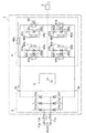
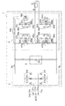
図1は、本発明の実施形態に係るリフティングマグネット用電源回路を示す回路図である。図1に示すリフティングマグネット用電源回路1は、リフティングマグネット2に電力の供給する電源回路である。リフティングマグネット用電源回路1は、直流変換部3と、Hブリッジ回路部4と、消磁用エネルギー吸収部5とを備え、リフティングマグネット2の励磁及び消磁を行う回路である。
FIG. 1 is a circuit diagram showing a lifting magnet power supply circuit according to an embodiment of the present invention. A lifting magnet power supply circuit 1 shown in FIG. 1 is a power supply circuit that supplies power to a lifting magnet 2. The lifting magnet power supply circuit 1 includes a DC converter 3, an H
直流変換部3は、3相交流電源ACG(発電機)から供給された交流電圧VAC1〜VAC3を直流電圧VDCに変換する。直流変換部3は、正側出力端3a及び負側出力端3bを有しており、生成した直流電源電圧VDCを正側出力端3aと負側出力端3bとの間に提供する。本実施形態では、正側出力端3aが高電位側電源として機能し、負側出力端3bが低電位側電源として機能する。なお、直流変換部3は、単相交流電源から交流電圧を直流電圧に変換する形態であってもよい。また、発電機が直流発電機である場合に、直流変換部は設けられていてもよい。
The DC converter 3 converts the AC voltages V AC1 to V AC3 supplied from the three-phase AC power supply ACG (generator) into a DC voltage V DC . The DC converter 3 has a
本実施形態の直流変換部3は、6個のダイオード31a〜31fを含むブリッジ回路によって構成されており、三相全波整流を行う。具体的には、ダイオード31a〜31fのうち、ダイオード31a及び31bが直列に接続され、ダイオード31c及び31dが直列に接続され、ダイオード31e及び31fが直列に接続されている。また、ダイオード31a及び31bからなる組と、ダイオード31c及び31dからなる組と、ダイオード31e及び31fからなる組とは、互いに並列に接続されている。そして、これらのダイオードの組のカソード側の一端は正側出力端30aに電気的に接続されており、アノード側の他端は負側出力端30bに電気的に接続されている。
The DC conversion unit 3 of the present embodiment is configured by a bridge circuit including six
また、ダイオード31aとダイオード31bとの間には、3相交流電源ACGにおける一相の電源端子から延びる交流電源ライン11aが電気的に接続されている。ダイオード31cとダイオード31dとの間には、3相交流電源ACGにおける他の一相の電源端子から延びる交流電源ライン11bが電気的に接続されている。ダイオード31eとダイオード31fとの間には、3相交流電源ACGにおける更に他の一相の電源端子から延びる交流電源ライン11cが電気的に接続されている。なお、直流変換部は、これ以外にも例えばサイリスタを用いた純ブリッジ回路や、ダイオード及びサイリスタを用いた混合ブリッジ回路によって構成されていてもよい。直流変換部が純ブリッジ回路や混合ブリッジ回路によって構成される場合、サイリスタは、図示しない位相制御回路によって所定の制御角で位相制御される。
An AC
Hブリッジ回路部4は、リフティングマグネット2の励磁及び消磁を制御する。Hブリッジ回路部4は、第1〜第4のスイッチング素子41a〜41dと、該第1〜第4のスイッチング素子41a〜41dそれぞれのドレイン−ソース間に電気的に接続された第1〜第4の転流用ダイオード(転流用機構、第1〜第4の整流素子)42a〜42dとを含むHブリッジ回路によって構成されている。
The H
具体的には、第1のスイッチング素子41aの一端は直流変換部3の正側出力端3aに接続されており、第1のスイッチング素子41aの他端は第2のスイッチング素子41bの一端に接続されている。第2のスイッチング素子41bの他端は直流変換部3の負側出力端3bに接続されている。一方、第3のスイッチング素子41cの一端は、直流変換部3の正側出力端3aに接続されており、第3のスイッチング素子41cの他端は第4のスイッチング素子41dの一端に接続されている。第4のスイッチング素子41dの他端は直流変換部3の負側出力端3bに接続されている。
Specifically, one end of the
また、第1,第2,第4の転流用ダイオード42a,42b,42dのアノードは、それぞれ第1,第2,第4のスイッチング素子41a,41b,41dの他端に接続されており、第1,第2,第4の転流用ダイオード42a,42b,42dのカソードは、それぞれ第1,第2,第4のスイッチング素子41a,41b,41dの一端に接続されている。そして、第1のスイッチング素子41aの他端及び第2のスイッチング素子41bの一端はリフティングマグネット2の一端に接続されており、第3のスイッチング素子41cの他端及び第4のスイッチング素子41dの一端はリフティングマグネット2の他端に接続されている。
The anodes of the first, second and
また、第3の転流用ダイオード42cのアノードは、それぞれ第3のスイッチング素子41cの他端に接続されており、第3の転流用ダイオード42cのカソードは、直流変換部3の正側出力端3a側、直接接続ではなく、抵抗素子46eを介して接続されている。リフティングマグネット2の全てのエネルギーを消磁用エネルギー吸収部5に戻すためには、大きなコンデンサ容量を必要とするので、抵抗素子46eで熱に変え必要量のみを消磁用エネルギー吸収部5に戻している。
The anode of the
第1〜第4のスイッチング素子41a〜41d各々の制御端子は図示しない制御回路に接続されており、第1〜第4のスイッチング素子41a〜41d各々における一端−他端間の導通状態は、該制御回路から提供される制御電流(または制御電圧)によって制御される。
The control terminals of the first to
第1〜第4のスイッチング素子41a〜41dは交流用有接点スイッチ(交流用電磁接触器)である。交流用有接点スイッチとしては、機械的に接触する接点を有するスイッチであって、交流用電磁接触器(MCスイッチ)などの機械式スイッチが適用可能である。
The first to
消磁用エネルギー吸収部5は、リフティングマグネット2の消磁を行う際にリフティングマグネット2に蓄積されたエネルギーを吸収するための回路部分である。消磁用エネルギー吸収部5は、直流変換部3の正側出力端3aと負側出力端3bとの間に接続されている。消磁用エネルギー吸収部5は、容量素子51を有している。なお、消磁用エネルギー吸収部5としては、様々な回路構成が適用可能である。
The demagnetizing energy absorbing unit 5 is a circuit part for absorbing energy accumulated in the lifting magnet 2 when the lifting magnet 2 is demagnetized. The demagnetizing energy absorbing unit 5 is connected between the
Hブリッジ回路部4は、スナバ回路45a〜45dを更に備えている。スナバ回路45a〜45dは、それぞれ、第1〜第4のスイッチング素子41a〜41dに並列に接続されている。
The H
スナバ回路45aは、抵抗素子46aと、容量素子47aと、ダイオード48aとを備えている。抵抗素子46aと容量素子47aとは直列に接続されており、抵抗素子46aにはダイオード48aが並列に接続されている。具体的には、ダイオード48aのアノードは抵抗素子46aと容量素子47aとの間のノードに接続されており、ダイオード48aのカソードは抵抗素子46aのもう一端に接続されている。なお、容量素子47aの容量は、例えば、100μFとされている。
The
同様に、スナバ回路45bは、抵抗素子46bと、容量素子47bと、ダイオード48bとを備えている。抵抗素子46bと容量素子47bとは直列に接続されており、抵抗素子46bにはダイオード48bが並列に接続されている。具体的には、ダイオード48bのアノードは抵抗素子46bと容量素子47bとの間のノードに接続されており、ダイオード48bのカソードは抵抗素子46bのもう一端に接続されている。なお、容量素子47bの容量は、例えば、100μFとされている。
Similarly, the
同様に、スナバ回路45cは、抵抗素子46cと、容量素子47cと、ダイオード48cとを備えている。抵抗素子46cと容量素子47cとは直列に接続されており、抵抗素子46cにはダイオード48cが並列に接続されている。具体的には、ダイオード48cのアノードは抵抗素子46cと容量素子47cとの間のノードに接続されており、ダイオード48cのカソードは抵抗素子46cのもう一端に接続されている。なお、容量素子47cの容量は、例えば、100μFとされている。
Similarly, the
同様に、スナバ回路45dは、抵抗素子46dと、容量素子47dと、ダイオード48dとを備えている。抵抗素子46dと容量素子47dとは直列に接続されており、抵抗素子46dにはダイオード48dが並列に接続されている。具体的には、ダイオード48のアノードは抵抗素子46dと容量素子47dとの間のノードに接続されており、ダイオード48dのカソードは抵抗素子46dのもう一端に接続されている。なお、容量素子47dの容量は、例えば、100μFとされている。
Similarly, the
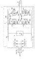
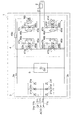
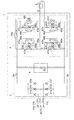
次に、図2〜5を参照しながら、リフティングマグネット用電源回路1の動作を説明する。図2〜5は、図1に示すリフティングマグネット用電源回路における各動作モードでの電流の流れを示す図である。 Next, the operation of the lifting magnet power supply circuit 1 will be described with reference to FIGS. 2 to 5 are diagrams showing current flows in the respective operation modes in the lifting magnet power supply circuit shown in FIG.
(リフティングマグネットの励磁動作モード)
Hブリッジ回路部4における第1のスイッチング素子41a及び第4のスイッチング素子41dを導通させる。これによって、図2に示すように、直流変換部3の正側出力端3a、第1のスイッチング素子41a、リフティングマグネット2、第4のスイッチング素子41d、直流変換部3の負側出力端3bに励磁電流I1が流れる。
(Excitation mode of lifting magnet)
The
次に、第1のスイッチング素子41aを非導通とする。これによって、図3に示すように、リフティングマグネット2、第4のスイッチング素子41d、第2の整流用ダイオード42bに還流電流I2が流れる。その後、再び第1のスイッチング素子41aを導通させる。これによって、図2に示すように、励磁電流I1が流れることとなる。
Next, the
このように、第1のスイッチング素子41aをスイッチングすることによって、リフティングマグネット2が励磁され、鉄片等を吸着して持ち上げることができる。なお、第4のスイッチング素子41dはスイッチング動作を行わない。
In this way, by switching the
(リフティングマグネットの消磁動作モード)
Hブリッジ回路部4における第1のスイッチング素子41a及び第4のスイッチング素子41dを非導通とし、リフティングマグネット2の両端電圧を反転させる。これによって、図4に示すように、リフティングマグネット2、第3のダイオード48c、消磁用エネルギー吸収部5における容量素子51、第2のダイオード48bに消磁電流I3が流れ、リフティングマグネット2に蓄積されたエネルギーが容量素子51に移乗すると共に容量素子51に蓄積される。
(Demagnetization mode of lifting magnet)
The
これにより、リフティングマグネット2が消磁され、吸着していた鉄片等を解放することができる。 As a result, the lifting magnet 2 is demagnetized, and the attracted iron pieces and the like can be released.
(リフティングマグネットの残留磁気の消磁動作モード)
ここで、リフティングマグネット2はヒステリシス特性によって残留磁気を有することとなる。そこで、Hブリッジ回路部4における第2のスイッチング素子41b及び第3のスイッチング素子41cを導通させる。これによって、図5に示すように、消磁用エネルギー吸収部5における容量素子51、第3のスイッチング素子41c、リフティングマグネット2、第2のスイッチング素子41bに残留磁気の消磁電流I4が流れる。すなわち、容量素子51に蓄積された電荷によって、リフティングマグネット2において消磁電流I3とは逆向きの残留磁気の消磁電流I4が流れる。
(Demagnetization mode of remanence of lifting magnet)
Here, the lifting magnet 2 has residual magnetism due to hysteresis characteristics. Therefore, the
これにより、リフティングマグネット2が消磁され、吸着していた鉄片等を解放することができる。この残留磁気の消磁の際、第2及び第3のスイッチング素子41b,41cはスイッチング動作を行わない。この第2及び第3のスイッチング素子41b,41cに、内部抵抗が比較的小さい有接点スイッチが用いられるので、発熱が低減されることとなる。
As a result, the lifting magnet 2 is demagnetized, and the attracted iron pieces and the like can be released. During the demagnetization of the residual magnetism, the second and
本実施形態に係るリフティングマグネット用電源回路1によれば、リフティングマグネット2への電力の供給を制御するHブリッジ回路部4において、転流用ダイオード42a〜42dを備えると共に、第1〜第4のスイッチング素子41a〜41d(交流用有接点スイッチ)に並列に接続されたスナバ回路45a〜45dを備える構成であるため、これらのスナバ回路45a〜45dによって、部品、配線により構成されるインダクタンスに溜まっている電気エネルギーを吸収して消費することができる。これにより、不要なアーク電圧を吸収して、接点を遮断するときのアークを使用上及び寿命上問題とならない大きさまで小さくすることが可能となる。第1〜第4のスイッチング素子41a〜41dにおけるアーク放電の発生を抑えることができる。これにより、リフティングマグネット2のように大きなインダクタンスを持つ負荷に流れる直流電流を、交流用の汎用接触器によって、オフすることができる。
According to the lifting magnet power supply circuit 1 according to the present embodiment, the H
また、リフティングマグネット用電源回路1では、スナバ回路45a〜45d、転流用ダイオード42a〜42d、交流用有接点スイッチ41a〜41dを備える構成であるため、発熱を抑えることが可能であり、従来必要であった冷却装置を不要とし、装置構成の簡素化を図ることができる。
The lifting magnet power supply circuit 1 includes
また、有接点スイッチは、従来の無接点スイッチと比較して、安価であり、メンテナンスも容易であるため、信頼性の向上及び低コスト化を図ることができる。また、アーク放電を吹き消すための装置も不要であるため、装置構成の簡素化、及び低コスト化を図ることができる。なお、有接点スイッチとは、交流用電磁接触器であり、機械的に接触する接点を有するスイッチであって、リレーなどの機械式スイッチである。 In addition, since the contact switch is less expensive and easier to maintain than the conventional contactless switch, the reliability can be improved and the cost can be reduced. In addition, since a device for blowing off arc discharge is unnecessary, the device configuration can be simplified and the cost can be reduced. In addition, a contact switch is an electromagnetic contactor for alternating current, a switch which has a contact which contacts mechanically, Comprising: It is mechanical switches, such as a relay.
なお、本発明は上記した本実施形態に限定されることなく種々の変形が可能である。上記実施形態のリフティングマグネット用電源回路1では、第1〜第4のスイッチング素子41a〜41dを有接点スイッチとしているが、第1〜第4のスイッチング素子のうち少なくとも一つが、有接点スイッチであり、有接点スイッチに並列に接続されたスナバ回路を更に備える構成であればよい。
The present invention is not limited to the above-described embodiment, and various modifications can be made. In the lifting magnet power supply circuit 1 of the above embodiment, the first to
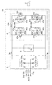
図6は、本発明の他の実施形態に係るリフティングマグネット用電源回路を示す回路図である。図6に示すリフティングマグネット用電源回路1Aが、図1に示すリフティングマグネット用電源回路1と違う点は、有接点スイッチである第1のスイッチング素子41aに代えて、無接点スイッチである第1のスイッチング素子49aを備える点である。
FIG. 6 is a circuit diagram showing a lifting magnet power supply circuit according to another embodiment of the present invention.
このように、第1のスイッチング素子49aは、スイッチング速度が比較的速い無接点スイッチであるので、リフティングマグネット2に印加する電圧の定電圧制御や電流の定電流制御の制御性を向上することができる。
Thus, since the
なお、第1のスイッチング素子41aのスイッチングの割合を調整することによって、リフティングマグネット2に印加する電圧を調整することができ、リフティングマグネット2に蓄積するエネルギーを調整することができる。これによって、例えば、鉄片の吸着の強度を調整することが可能となる。本実施形態では、第1のスイッチング素子41aのスイッチング速度が比較的速いので、このような調整の制御性をも向上することが可能である。
The voltage applied to the lifting magnet 2 can be adjusted by adjusting the switching rate of the
また、直流変換部3におけるダイオード31a〜31f、Hブリッジ回路部4における第1〜第4のダイオード42a〜42dは、一方向に整流機能を備えていればダイオード以外の素子でも代用可能である。
The
また、上記実施形態では、CRD型スナバ回路を例示したが、スナバ回路45a〜45dは本実施形態に限られない。例えば、容量素子(C)のみで構成されたスナバ回路であってもよいし、容量素子と抵抗素子(R)との組合せで構成されたスナバ回路であってもよい。また、複数の容量素子を備えるスナバ回路でもよい。また、容量素子の容量は、スナバ回路ごとに異なっていてもよい。
Moreover, in the said embodiment, although the CRD type snubber circuit was illustrated,
また、上記実施形態では、転流用機構として、ダイオード42a〜42dを例示したが、スイッチング素子を転流用機構として用いてもよい。 Moreover, in the said embodiment, although diode 42a-42d was illustrated as a mechanism for commutation, you may use a switching element as a mechanism for commutation.
1,1A…リフティングマグネット用電源回路、2…リフティングマグネット、3…直流変換部、4…Hブリッジ回路部、5…消磁用エネルギー吸収部、31a〜31f…ダイオード、41a〜41d…スイッチング素子(有接点スイッチ)、42a〜42d…転流用ダイオード(転流用機構)、45a〜45d…スナバ回路、46a〜46d…抵抗素子、47a〜47d…容量素子、49a…スイッチング素子(無接点スイッチ)、51…容量素子。
DESCRIPTION OF
Claims (1)
高電位側電源と低電位側電源との間に順に直列に接続された第1及び第2のスイッチング素子であって、その間のノードが前記リフティングマグネットの一端に接続される前記第1及び第2のスイッチング素子と、前記高電位側電源と前記低電位側電源との間に順に直列に接続された第3及び第4のスイッチング素子であって、その間のノードが前記リフティングマグネットの他端に接続される前記第3及び第4のスイッチング素子と、転流用機構とを有し、前記リフティングマグネットへの電力の供給を制御するHブリッジ回路部を備え、
前記第1のスイッチング素子は、無接点スイッチであり、
前記第2〜第4のスイッチング素子は、交流用有接点スイッチであり、
前記交流用有接点スイッチに並列に接続されたスナバ回路を更に備えることを特徴とするリフティングマグネット用電源回路。
A lifting magnet power supply circuit for supplying power to the lifting magnet,
First and second switching elements connected in series between a high-potential-side power supply and a low-potential-side power supply in series, and a node between them is connected to one end of the lifting magnet. Switching elements, and third and fourth switching elements connected in series between the high-potential-side power supply and the low-potential-side power supply in order, and a node between them is connected to the other end of the lifting magnet The third and fourth switching elements, and a commutation mechanism, comprising an H-bridge circuit section for controlling power supply to the lifting magnet,
The first switching element is a contactless switch;
The second to fourth switching element is a contact switch AC,
A power supply circuit for a lifting magnet, further comprising a snubber circuit connected in parallel to the AC contact switch.
Priority Applications (2)
| Application Number | Priority Date | Filing Date | Title |
|---|---|---|---|
| JP2009087558A JP5117438B2 (en) | 2009-03-31 | 2009-03-31 | Power supply circuit for lifting magnet |
| CN2010101548250A CN101850927B (en) | 2009-03-31 | 2010-03-30 | Suspended magnet power circuit |
Applications Claiming Priority (1)
| Application Number | Priority Date | Filing Date | Title |
|---|---|---|---|
| JP2009087558A JP5117438B2 (en) | 2009-03-31 | 2009-03-31 | Power supply circuit for lifting magnet |
Publications (2)
| Publication Number | Publication Date |
|---|---|
| JP2010235293A JP2010235293A (en) | 2010-10-21 |
| JP5117438B2 true JP5117438B2 (en) | 2013-01-16 |
Family
ID=42802645
Family Applications (1)
| Application Number | Title | Priority Date | Filing Date |
|---|---|---|---|
| JP2009087558A Active JP5117438B2 (en) | 2009-03-31 | 2009-03-31 | Power supply circuit for lifting magnet |
Country Status (2)
| Country | Link |
|---|---|
| JP (1) | JP5117438B2 (en) |
| CN (1) | CN101850927B (en) |
Families Citing this family (3)
| Publication number | Priority date | Publication date | Assignee | Title |
|---|---|---|---|---|
| CN102897642B (en) * | 2011-07-26 | 2014-10-01 | 宝山钢铁股份有限公司 | Capacitor inversion type magnetizing and demagnetizing lifting electromagnet |
| CN102897643B (en) * | 2011-07-26 | 2014-10-01 | 宝山钢铁股份有限公司 | Electromagnet coil tap type magnetizing and demagnetizing lifting electromagnet |
| JP6734496B1 (en) | 2020-04-17 | 2020-08-05 | 三菱重工環境・化学エンジニアリング株式会社 | Screen device, concentration system, dehydration system, and water treatment system |
Family Cites Families (15)
| Publication number | Priority date | Publication date | Assignee | Title |
|---|---|---|---|---|
| JPS60144288A (en) * | 1983-12-29 | 1985-07-30 | 神鋼電機株式会社 | Power supply circuit for hanging electromagnet |
| JPS61156491U (en) * | 1985-03-20 | 1986-09-27 | ||
| EP0262521B1 (en) * | 1986-09-30 | 1991-04-17 | Siemens Aktiengesellschaft | Device for controlling the electrical voltage at the rotating exciter winding of an electrical generator |
| JPH06104289B2 (en) * | 1988-07-20 | 1994-12-21 | フジ磁工株式会社 | Degaussing device for electromagnetic chuck |
| US5317122A (en) * | 1992-01-28 | 1994-05-31 | Mitsubishi Denki Kabushiki Kaisha | Discharge-processing electric power-source assembly |
| JPH08255670A (en) * | 1995-03-20 | 1996-10-01 | Juki Corp | Electric heater drive |
| JPH09245586A (en) * | 1996-03-12 | 1997-09-19 | Tai-Haa Yan | Arc-extinguishing circuit device for cutting off dc power source |
| JPH10174424A (en) * | 1996-10-07 | 1998-06-26 | Toshiba Corp | Power converter |
| US5841647A (en) * | 1996-10-07 | 1998-11-24 | Kabushiki Kaisha Toshiba | Power conversion system |
| JP2000036238A (en) * | 1998-04-06 | 2000-02-02 | Shigeisa Imoto | Switch circuit |
| JP2000153983A (en) * | 1998-11-18 | 2000-06-06 | Sakato Kosakusho:Kk | Power circuit for lifting magnet |
| JP2000156967A (en) * | 1998-11-19 | 2000-06-06 | Meidensha Corp | Turn-on test circuit for current driving type power semiconductor element |
| JP3395145B2 (en) * | 2000-03-17 | 2003-04-07 | 住友重機械工業株式会社 | Lifting magnet device |
| JP4335198B2 (en) * | 2005-10-27 | 2009-09-30 | 住友重機械工業株式会社 | Lifting magnet drive circuit |
| JP2007301703A (en) * | 2006-05-15 | 2007-11-22 | Ryobi Ltd | Electric power tool |
-
2009
- 2009-03-31 JP JP2009087558A patent/JP5117438B2/en active Active
-
2010
- 2010-03-30 CN CN2010101548250A patent/CN101850927B/en active Active
Also Published As
| Publication number | Publication date |
|---|---|
| JP2010235293A (en) | 2010-10-21 |
| CN101850927B (en) | 2012-11-14 |
| CN101850927A (en) | 2010-10-06 |
Similar Documents
| Publication | Publication Date | Title |
|---|---|---|
| CN112564582B (en) | Demagnetization of the rotor of a separately excited synchronous machine | |
| US10978258B2 (en) | Direct current circuit breaker device | |
| KR20140084795A (en) | Bypass apparatus for converter | |
| JP5117438B2 (en) | Power supply circuit for lifting magnet | |
| JP4607199B2 (en) | Lifting magnet drive circuit | |
| CN100474478C (en) | Drive circuit of DC voltage driven magnet contactor and power converter | |
| JP2009208931A (en) | Lifting magnet driving circuit | |
| KR101427342B1 (en) | Load-Segmentation-Based Full Bridge Inverter and Method for Controlling Same | |
| JP2010207010A (en) | Coil switching device of three-phase ac motor drive system | |
| CN102017584A (en) | System and method for quickly discharging a DC relay | |
| JP2018201326A (en) | Discharge device | |
| KR20140136645A (en) | Power Supply Circuit for Lifting Magnet | |
| JP4335198B2 (en) | Lifting magnet drive circuit | |
| JP4015583B2 (en) | Superconducting coil energy storage circuit | |
| US20190044347A1 (en) | Multiple output battery system | |
| JP2010100437A (en) | Lifting magnet driving circuit | |
| JP2013199372A (en) | Power source circuit for lifting magnet | |
| CN116762270A (en) | De-excitation systems for inductive circuits | |
| JP4030349B2 (en) | Power circuit | |
| JP6746864B2 (en) | Control system for switching DC-DC voltage converter from buck operation mode to safe operation mode | |
| JP5311192B2 (en) | Lifting magnet power supply | |
| JP2007161402A (en) | Lifting magnet driving circuit | |
| TW201442936A (en) | Power supply circuit of lifting magnet | |
| JP2010179978A (en) | Lifting magnet control system and lifting magnet control method | |
| JP7801990B2 (en) | Power Conversion Device |
Legal Events
| Date | Code | Title | Description |
|---|---|---|---|
| A977 | Report on retrieval |
Free format text: JAPANESE INTERMEDIATE CODE: A971007 Effective date: 20110118 |
|
| A131 | Notification of reasons for refusal |
Free format text: JAPANESE INTERMEDIATE CODE: A131 Effective date: 20110125 |
|
| A131 | Notification of reasons for refusal |
Free format text: JAPANESE INTERMEDIATE CODE: A131 Effective date: 20110927 |
|
| A02 | Decision of refusal |
Free format text: JAPANESE INTERMEDIATE CODE: A02 Effective date: 20120529 |
|
| A521 | Written amendment |
Free format text: JAPANESE INTERMEDIATE CODE: A523 Effective date: 20120824 |
|
| A911 | Transfer of reconsideration by examiner before appeal (zenchi) |
Free format text: JAPANESE INTERMEDIATE CODE: A911 Effective date: 20120831 |
|
| TRDD | Decision of grant or rejection written | ||
| A01 | Written decision to grant a patent or to grant a registration (utility model) |
Free format text: JAPANESE INTERMEDIATE CODE: A01 Effective date: 20121016 |
|
| A01 | Written decision to grant a patent or to grant a registration (utility model) |
Free format text: JAPANESE INTERMEDIATE CODE: A01 |
|
| A61 | First payment of annual fees (during grant procedure) |
Free format text: JAPANESE INTERMEDIATE CODE: A61 Effective date: 20121017 |
|
| R150 | Certificate of patent or registration of utility model |
Ref document number: 5117438 Country of ref document: JP Free format text: JAPANESE INTERMEDIATE CODE: R150 Free format text: JAPANESE INTERMEDIATE CODE: R150 |
|
| FPAY | Renewal fee payment (event date is renewal date of database) |
Free format text: PAYMENT UNTIL: 20151026 Year of fee payment: 3 |