JP5117817B2 - Multi-level voltage generator, data driver, and liquid crystal display device - Google Patents
Multi-level voltage generator, data driver, and liquid crystal display device Download PDFInfo
- Publication number
- JP5117817B2 JP5117817B2 JP2007281525A JP2007281525A JP5117817B2 JP 5117817 B2 JP5117817 B2 JP 5117817B2 JP 2007281525 A JP2007281525 A JP 2007281525A JP 2007281525 A JP2007281525 A JP 2007281525A JP 5117817 B2 JP5117817 B2 JP 5117817B2
- Authority
- JP
- Japan
- Prior art keywords
- resistor
- connection portion
- conductor
- level voltage
- voltage generator
- Prior art date
- Legal status (The legal status is an assumption and is not a legal conclusion. Google has not performed a legal analysis and makes no representation as to the accuracy of the status listed.)
- Expired - Fee Related
Links
Images







Landscapes
- Liquid Crystal Display Device Control (AREA)
- Liquid Crystal (AREA)
- Control Of Indicators Other Than Cathode Ray Tubes (AREA)
Description
本発明は、マルチレベル電圧発生器、それを用いたデータドライバ、及び液晶表示装置に関し、特に、マルチレベル電圧発生器における抵抗ストリングのレイアウトパターンに関する。 The present invention relates to a multilevel voltage generator, a data driver using the same, and a liquid crystal display device, and more particularly to a layout pattern of a resistor string in the multilevel voltage generator.
抵抗ストリングは、複数の分圧電極を介して接続される複数の抵抗を備え、入力される参照電圧を分圧し、複数の分圧電極のそれぞれから分圧電圧(レベル電圧)を出力する。従来技術による抵抗ストリングのレイアウトパターンの一例として、特開平8−213912号公報に記載の抵抗ストリングについて説明する(特許文献1参照)。特許文献1に記載の抵抗ストリングは、1つの抵抗素子に等間隔にコンタクト及び電極が設けられ、そこから分圧電圧を出力する。図14は、特許文献1に記載の抵抗ストリングのレイアウトパターンを示す平面図である。
The resistor string includes a plurality of resistors connected via a plurality of voltage dividing electrodes, divides an input reference voltage, and outputs a divided voltage (level voltage) from each of the plurality of voltage dividing electrodes. As an example of a conventional resistor string layout pattern, a resistor string described in JP-A-8-213912 will be described (see Patent Document 1). In the resistor string described in
図14を参照して、従来技術による抵抗ストリング50は、1つの抵抗素子55にN+1個のコンタクト54−0〜54−Nが等間隔に設けられている。抵抗ストリング50は、コンタクト54−0及び54−Nのそれぞれに入力される参照電圧VG0及びVGNの電位差を分圧し、コンタクト54−0〜54−Nを介して分圧電圧V0〜VNを出力する。詳細には、コンタクト54−0には、参照電圧VG0が入力される配線51が接続され、コンタクト54−Nには、参照電圧VGNが入力される配線52が接続される。コンタクト54−1〜54−(N−1)のそれぞれには、配線53−1〜53−(N−1)が接続される。このような構成により、入力される2つの参照電圧VG0及びVGNの電位差は、それぞれのコンタクト間(分圧電極間)の抵抗Rにより分圧され、分圧電圧V1〜VN−1としてノード56−1〜56−(N−1)に供給される。又、入力される参照電圧VG0及びVGNはそれぞれ、配線51及び52を介し、分圧電圧V0及びVNとしてノード5−0及び56−Nに供給される。
Referring to FIG. 14, in a
近年、高精度な分圧電圧が要求されており、分圧抵抗の精度を向上させる技術が要求されている。このため、分圧抵抗の精度を向上させるため、1つの抵抗素子ではなく複数の抵抗素子を分圧電極を介して接続した抵抗ストリングが、特開2000−208703号公報の従来技術として記載されている(特許文献2参照)。更に、特許文献2には、分極電極を取り出すパターンを低抵抗素子にすることで、コンタクトにおける抵抗(以下コンタクト抵抗と称す)のバラツキを回避して分圧電圧の精度を高める技術が記載されている。
一方、液晶表示装置代表される表示装置の表示ムラを軽減するため、高精度な階調電圧が要求されている。特に、階調電圧発生回路によって生成される階調電圧と、所望の階調電圧のガンマカーブとの誤差を軽減する技術が求められている。 On the other hand, in order to reduce display unevenness of a display device typified by a liquid crystal display device, a highly accurate gradation voltage is required. In particular, there is a need for a technique for reducing an error between a gradation voltage generated by a gradation voltage generation circuit and a gamma curve of a desired gradation voltage.
しかし、従来技術による抵抗ストリングは、参照電圧が入力されるコンタクトのコンタクト抵抗により、分圧に寄与する分圧電極間の抵抗(以下、分割抵抗と称す)に差が生じていた。このため、従来技術による抵抗ストリングを階調電圧発生回路に用いると、階調電圧の精度が低くなり、所望のガンマカーブに対応する階調電圧を得ることが困難であった。以下、図14及び図15を参照して、従来技術による抵抗ストリングの分圧電圧(階調電圧)の誤差について説明する。 However, the resistance string according to the prior art has a difference in resistance between voltage dividing electrodes (hereinafter referred to as divided resistance) that contributes to voltage division due to the contact resistance of a contact to which a reference voltage is input. For this reason, when the resistor string according to the prior art is used for the gradation voltage generating circuit, the precision of the gradation voltage is lowered, and it is difficult to obtain the gradation voltage corresponding to the desired gamma curve. Hereinafter, with reference to FIGS. 14 and 15, an error in the divided voltage (gradation voltage) of the resistor string according to the conventional technique will be described.
図15は、図14に示す抵抗ストリング50の等価回路である。図14を参照して、安定状態において、参照電圧による定電流Iは、配線51からコンタクト54−0及び54−Nを介して配線52に至る経路を流れる。このため、図15に示すように、電流経路上にコンタクト54−0及び54−Nによるコンタクト抵抗rcon0及びrconNが形成されることになる。コンタクト抵抗rcon0及びrconNを考慮しない場合、抵抗Rのみで参照電圧は分圧され、生成された分圧電圧V0〜VNは所望の値(理想値)で出力される。しかし、実際の分圧電圧V1〜VN−1はコンタクト抵抗rcon0及びrconNによる電圧降下の影響を受ける一方、階調電圧V0及びVNは、VG0及びVGNがそのまま出力される。このため、従来技術による抵抗ストリングでは、分圧電圧V0〜VN間の相対誤差が大きくなってしまう。又、このrcon0〜rconNは製造時のばらつきによって製品毎、及びコンタクト毎に異なる値をとる可能性があるため、コンタクト抵抗を見込んで設計しても設計通りの階調電圧出力を得られず、表示特性を悪化させることがある。又は、この問題を避けるために製品の選別規格を厳しくすると、製品の歩留まりを下げてしまうことがある。
FIG. 15 is an equivalent circuit of the
上述のような問題は、特許文献2に記載の抵抗ストリングにも、複数の抵抗素子を接続して構成された抵抗ストリングにも同様に発生する。特に複数の抵抗素子を接続して構成された抵抗ストリングでは、抵抗素子を接続するコンタクトの製造バラツキのため、それぞれのコンタクト抵抗に差が生じ、各階調電圧の相対誤差は更に増大する。
The above-described problem occurs in the resistance string described in
以下に、[発明を実施するための最良の形態]で使用される番号・符号を括弧付きで用いて、[課題を解決するための手段]を説明する。この番号・符号は、[特許請求の範囲]の記載と[発明を実施するための最良の形態]の記載との対応関係を明らかにするために付加されたものであるが、[特許請求の範囲]に記載されている発明の技術的範囲の解釈に用いてはならない。 [Means for Solving the Problems] will be described below using the numbers and symbols used in [Best Mode for Carrying Out the Invention] in parentheses. This number / symbol is added to clarify the correspondence between the description of [Claims] and the description of the best mode for carrying out the invention. It should not be used for interpreting the technical scope of the invention described in [Scope].
本発明によるマルチレベル電圧発生器(22)は、供給される第1の参照電圧(VG0)と第2の参照電圧(VGN)とに応じた複数のレベル電圧(V0〜VN)を生成するマルチレベル電圧発生器である。マルチレベル電圧発生器(22)は、抵抗体(7)と、第1の参照電圧(VG0)が供給される第1の導電体(10)と、第2の参照電圧(VGN)が供給される第2の導電体(11)と、複数のレベル電圧(V0〜VN)のうち第1の参照電圧(VG0)に最も近い値の第1のレベル電圧(V0)が出力される第3の導電体(1)と、第1のレベル電圧(V0)とは別の第2のレベル電圧(例えばVN−1)が出力される第4の導電体(3−(N−1)とを具備する。この際、第1乃至第4の導電体(1、10、3―(N−1)、11)のそれぞれは、分離して形成される。更に、マルチレベル電圧発生器(22)は、第1の導電体(10)と抵抗体(7)とを結合して導通可能とする第1の接続部(8)と、第2の導電体(11)と抵抗体(7)とを結合して導通可能とする第2の接続部(9)と、第3の導電体(1)と抵抗体(7)とを結合して導通可能とする第3の接続部(4)と、第4の導電体(3−(N−1)と抵抗体(7)とを結合して導通可能とする第4の接続部(6−(N−1)とを具備する。ここで、第3の接続部(4)、第1の接続部(8)、第4の接続部(6−(N−1))、第2の接続部(9)は、直列形態の第1から第3の抵抗領域(rdum及びR)を形成するように、抵抗体(7)に順次配置される。 Multilevel voltage generator according to the present invention (22), a first reference voltage to be supplied (VG 0) and a second reference voltage (VG N) and a plurality of level voltage corresponding to (V 0 ~V N) Is a multi-level voltage generator. The multi-level voltage generator (22) includes a resistor (7), a first conductor (10) to which a first reference voltage (VG 0 ) is supplied, and a second reference voltage (VG N ). The supplied second conductor (11) and the first level voltage (V 0 ) having a value closest to the first reference voltage (VG 0 ) among the plurality of level voltages (V 0 to V N ) The third conductor (1) to be output and the fourth conductor (3 -N ) that outputs a second level voltage (for example, V N-1 ) different from the first level voltage (V 0 ). In this case, each of the first to fourth conductors (1, 10, 3- (N-1), 11) is formed separately. The level voltage generator (22) combines the first conductor (10) and the resistor (7) to enable conduction, and the second conductor (1). 1) and the resistor (7) are coupled to enable conduction, and the second connection portion (9) that allows conduction and the third conductor (1) and resistor (7) are coupled to enable conduction. The third connection portion (4), the fourth conductor (3- (N-1), and the resistor (7) are coupled to each other to enable conduction. Here, the third connecting portion (4), the first connecting portion (8), the fourth connecting portion (6- (N-1)), and the second connecting portion (9). Are sequentially arranged on the resistor (7) so as to form first to third resistance regions (r dum and R) in series.
このような構成により、第1及び第2の参照電圧(VG0及びVGN)に基づく定電流(I)が、第1の接続部(8)と第2の接続部(9)との間に形成される第2及び第3の抵抗領域(R)のみを流れる。このため、参照電圧が供給される接続部(8、9)のコンタクト抵抗による影響が、全てのレベル電圧(V0〜VN)に一律に作用する。 With such a configuration, a constant current (I) based on the first and second reference voltages (VG 0 and VG N ) is generated between the first connection portion (8) and the second connection portion (9). Only the second and third resistance regions (R) formed in For this reason, the influence by the contact resistance of the connection parts (8, 9) to which the reference voltage is supplied acts uniformly on all the level voltages (V 0 to V N ).
又、本発明によるマルチレベル電圧発生器(22)は、階調電圧発生回路として、データドライバ(20)に適用されることが好ましい。この場合、データドライバ(20)は、入力されるデジタルデータに応じてマルチレベル電圧発生器(22)から出力されるレベル電圧(V0〜VN)を選択するデコーダ(25)と、デコーダ(25)で選択されたレベル電圧を増幅出力する増幅器(26)とを具備する。 Further, the multi-level voltage generator (22) according to the present invention is preferably applied to the data driver (20) as a gradation voltage generating circuit. In this case, the data driver (20) includes a decoder (25) for selecting a level voltage (V 0 to V N ) output from the multi-level voltage generator (22) according to input digital data, and a decoder ( And an amplifier (26) for amplifying and outputting the level voltage selected in 25).
更に、マルチレベル電圧発生器(22)を利用したデータドライバ(20)は、液晶表示装置(100)に適用されることが好ましい。この場合、液晶表示装置(100)は、上述のデータドライバ(100)と、走査線(47)とデータ線(46)とに接続された画素(P)を有する表示パネル(40)と、走査線(47)を駆動するゲートドライバ(30)とを具備する。 Further, the data driver (20) using the multi-level voltage generator (22) is preferably applied to the liquid crystal display device (100). In this case, the liquid crystal display device (100) includes the above-described data driver (100), a display panel (40) having pixels (P) connected to the scanning lines (47) and the data lines (46), and scanning. And a gate driver (30) for driving the line (47).
本発明によるマルチレベル電圧発生器によれば、出力する複数のレベル電圧における相対誤差を抑制することができる。 According to the multilevel voltage generator of the present invention, it is possible to suppress relative errors in a plurality of level voltages to be output.
又、本発明によるマルチレベル電圧発生器を階調電圧発生回路として用いたデータドライバ及び液晶表示装置によれば、表示ムラを低減することができる。 Further, according to the data driver and the liquid crystal display device using the multi-level voltage generator according to the present invention as the gradation voltage generating circuit, display unevenness can be reduced.
又、マルチレベル電圧発生器、これを用いたデータドライバ、及び液晶表示装置の歩留まりを向上できる。 Further, the yield of the multilevel voltage generator, the data driver using the same, and the liquid crystal display device can be improved.
以下、添付図面を参照して、本発明による階調電圧発生回路、及び抵抗ストリングのレイアウトパターンの実施の形態が説明される。本実施の形態では、マルチレベル電圧発生器として液晶表示装置のデータドライバに他の回路と一体で形成され、データ線(画素)を駆動するための階調電圧を生成する階調電圧発生回路を一例に、抵抗ストリングのレイアウトパターンを説明する。レイアウトパターンは、半導体基板や絶縁性基板等の上に薄膜材料を積層して素子及び回路が形成されるプロセスにおいて、露光装置等で用いられるマスクのパターンに対応する。尚、以下では、同一構成及び信号には同一符号を付し、同一構成が複数の場合、追い番を付して説明する。又、複数の構成を総称する場合は、追い番を除いた符号で説明する。 Hereinafter, embodiments of a grayscale voltage generation circuit and a layout pattern of resistor strings according to the present invention will be described with reference to the accompanying drawings. In this embodiment, a gradation voltage generation circuit that is formed integrally with other circuits in a data driver of a liquid crystal display device as a multi-level voltage generator and generates a gradation voltage for driving a data line (pixel). As an example, a layout pattern of resistor strings will be described. The layout pattern corresponds to a mask pattern used in an exposure apparatus or the like in a process in which elements and circuits are formed by laminating a thin film material on a semiconductor substrate, an insulating substrate, or the like. In the following description, the same components and signals are denoted by the same reference numerals, and when there are a plurality of the same components, a serial number is assigned for explanation. In addition, when a plurality of configurations are collectively referred to, they will be described with reference numerals excluding the serial number.
1.液晶表示装置100の構成
図1及び図2を参照して、本発明による階調電圧発生回路22を利用する液晶表示装置100の構成を説明する。図1は、液晶表示装置100の構成を示すブロック図である。液晶表示装置100は、データドライバ20、ゲートドライバ30、及び表示パネル40を具備する。表示パネル40には、互いに直交する複数のデータ線46と複数の走査線47の交点領域に画素Pが設けられる。図1には、データ線46、走査線47、画素Pはそれぞれ1つのみが示されているが、実際の表示パネル40には、複数のデータ線46及びゲート線47が設けられ、複数の画素Pがマトリックス状に設けられる。データドライバ20は、データ線46に対しデータ信号Voutを出力し、画素Pを駆動する。ゲートドライバ30は、ゲート線47を駆動して、データ信号Voutを書き込む画素Pを決定する。画素Pは、TFT48と、TFT48の一端である画素電極44と対向電極45との間に接続された液晶容量43とを備える。ゲートドライバ30によってTFT48がターンオンされた状態で、データ線46を介してデータ信号Voutが供給されると、液晶容量43にデータ信号Voutが書き込まれる。
1. Configuration of Liquid
図2は、データドライバ20の構成を示すブロック図である。データドライバ20は、階調電圧回路22、ラッチアドレスセレクタ23、ラッチ24、デコーダ25、増幅器26を備える。ラッチアドレスセレクタ23は、クロックCLKに応じたタイミングで、ラッチ24に対し駆動する画素Pのアドレスを指定する。ラッチ24は、入力される映像データをストローブ信号STBに応じてBビットのデータ信号としてデコーダ25に出力する。階調電圧発生回路22は、データ線44を駆動するための階調電圧V0〜VNをデコーダ25に供給する。詳細には、階調電圧発生回路22は、入力する参照電圧(ガンマ電圧)VG0及びVGNに応じた階調電圧V0〜VNを出力する抵抗ストリング21を備える。デコーダ25及び増幅器26は、複数のデータ線46に対応して複数設けられる。抵抗ストリング21は、階調電圧V0〜VNを出力するノード14−0〜14−Nを有し、図示しないスイッチ回路を介して複数のデコーダ25のそれぞれに接続される。デコーダ25は、ラッチ24からのデータ信号に応じた階調電圧を階調電圧V0〜VNから選択し、データ信号Voutとしてデータ線44に出力する。
FIG. 2 is a block diagram showing the configuration of the
ここで、デコーダ25で選択された階調電圧は、増幅器26の図示しない差動増幅器の入力端(例えば差動対を構成するトランジスタのゲート端子)に供給される。すなわち、ノード14−0〜14−Nは、容量性負荷(差動対を構成するトランジスタのゲート容量)と接続することなり、ノード14−0〜14−Nと増幅器26の入力端との間に定電流(静消費電流)は流れない(ただし、充分な時間の経過後)。又、デコーダ25で同時に選択される階調電圧は複数でも構わない。この際、選択された階調電圧を出力するノード14は、増幅器26内の差動増幅器の複数の入力端と接続するが、上述と同様に、ノード14と差動増幅器の入力端との間に定電流は流れない。
Here, the gradation voltage selected by the
2.第1の実施の形態
図3から図5を参照して、図2に示す本発明による抵抗ストリング21の第1の実施の形態を説明する。以下の実施の形態では、一続きの1つの抵抗素子とコンタクトとを利用して分割抵抗を形成し、参照電圧に応じた階調電圧を生成する抵抗ストリングについて説明する。
2. First Embodiment A first embodiment of a
(抵抗ストリング21のレイアウトパターン)
図3は、抵抗ストリング21のレイアウトパターンを示す平面図である。図4は、抵抗ストリング21を立体的に見たときの斜視図である。図3及び図4を参照して、抵抗ストリング21は、1つの抵抗素子7に供給される参照電圧VG0及びVGNに応じた階調電圧V0〜VNが、コンタクト4、6−1〜6−(N−1)、5のそれぞれを介してノード14−0〜14−Nに出力される。詳細には、1つの抵抗素子7にコンタクト8及び9が設けられ、それぞれ配線10及び11を介して参照電圧VG0及びVGNが入力される。又、抵抗素子7上におけるコンタクト8とコンタクト9との間に、N−1個のコンタクト6−1〜6−(N−1)が等間隔に設けられ、各コンタクト間の抵抗素子によって抵抗Rが形成される。本実施の形態におけるコンタクト6−1〜6−(N−1)は、抵抗素子7におけるコンタクト8とコンタクト9とを結ぶ最短距離の線上の領域に設けられる。コンタクト6−1〜6−(N−1)のそれぞれには配線3−1〜3−(N−1)が接続され、そこから階調電圧V1〜VN−1が、ノードN14−1〜14−(N−1)へ供給される。尚、図4において、各コンタクトの高さは等しくなくてもよい。又、各配線は抵抗素子7の上ではなく、下にあってもよい。
(Layout pattern of resistor string 21)
FIG. 3 is a plan view showing a layout pattern of the
又、階調電圧V0及びVNを取り出すためのコンタクト4及び5が、コンタクト8とコンタクト9との間の領域の外側にある抵抗素子7に設けられる。例えば図3に示すように、コンタクト8を挟んでコンタクト6−1に対向する抵抗素子7の領域にコンタクト4が設けられる。この際、コンタクト4とコンタクト8との間隔は充分小さいことが好ましい。同様に、コンタクト9を挟んでコンタクト6−Nに対向する抵抗素子7の領域にコンタクト5が設けられ、コンタクト5とコンタクト9との間隔は充分小さいことが好ましい。ここで、コンタクト4とコンタクト8との間、コンタクト5とコンタクト9との間には抵抗素子によってダミー抵抗rdumが形成される。このダミー抵抗rdumは、ほとんど0に等しいことが好ましい。コンタクト4には、配線1が接続され、配線1を介してVG0とほぼ等しい値の階調電圧V0がノード14−0に供給される。同様に、コンタクト5には、配線2が接続され、配線2を介してVGNとほぼ等しい値の階調電圧VNがノード14−Nに供給される。
Further,
ここで、参照電圧VG0は、参照電圧VGNより大きい電圧値とすると、階調電圧V0は、階調電圧の最大値、階調電圧VNは階調電圧の最小値となる。すなわち、本発明では、階調電圧の最大値及び最小値の取り出し口となるコンタクト4及び5が、参照電圧の供給口であるコンタクト8とコンタクト9との間の領域の外側に設けられる。換言すると、参照電圧VG0及びVGNに最も近い階調電圧V0及びVNの取り出し口となるコンタクト4及び5が、コンタクト8及び9の間の領域の外側に設けられる。尚、コンタクト6−1〜6−(N−1)が、コンタクト8とコンタクト9とを結ぶ最短距離の線上の領域に設けられると、回路面積を縮小できるため、面積コスト上有利である。
Here, if the reference voltage VG 0 is a voltage value greater than the reference voltage VG N , the gradation voltage V 0 is the maximum value of the gradation voltage, and the gradation voltage V N is the minimum value of the gradation voltage. In other words, in the present invention, the
ここで、配線1、2、3−1〜3−(N−1)及び配線10、11は、金属配線が好ましく、配線1と配線10、配線2と配線11はそれぞれ分離している。
Here, the
(抵抗ストリング21の動作)
上述のような構成により、抵抗ストリング21は、参照電圧VG0及びVGNに応じた階調電圧V0〜VNをノード140〜14Nに供給する。この際、ノード14−0〜14−Nには、増幅器26内の容量性負荷(差動対を構成するトランジスタのゲート容量)が接続されるため、安定状態では、コンタクト4、6−1〜6−(N−1)、5からノード14−0〜14−Nに至る経路には定電流(静消費電流)は流れない。一方、参照電圧VG0と参照電圧VGNとの電位差に応じて、コンタクト8とコンタクト9との間に定電流Iが流れる。この際、定電流Iは、コンタクト8から、コンタクト6−1〜6−(N−1)を経由してコンタクト9に至る経路を流れる。しかし、コンタクト4及び5は、コンタクト8とコンタクト9との間に設けられていないため、定電流Iの経路上から外れる。
(Operation of the resistor string 21)
With the configuration as described above, the
図5は、第1の実施の形態における抵抗ストリング21の等価回路である。図5を参照して、抵抗ストリング21におけるコンタクト抵抗の影響について説明する。ここで、コンタクト8及び9による抵抗をそれぞれコンタクト抵抗rconH、rconLとし、コンタクト4及び5による抵抗をそれぞれコンタクト抵抗rcon0及びrconNとし、コンタクト6−1〜6−(N−1)による抵抗をそれぞれコンタクト抵抗rcon1〜rconN−1とする。
FIG. 5 is an equivalent circuit of the
図5を参照して、ノード17とノード18との間には、抵抗素子7によるN個の抵抗Rが直列に接続される。各抵抗R間の接続点は、コンタクト抵抗rcon1〜rconN−1を介してノード14−1〜14−(N−1)に接続される。又、ノード17は、ダミー抵抗rdum及びコンタクト抵抗rcon0を介してノード14−0に接続され、ノード18は、ダミー抵抗rdum及びコンタクト抵抗rconNを介してノード14−Nに接続される。更に、ノード17には、コンタクト抵抗rconHを介して参照電圧VG0が供給され、ノード18には、コンタクトrconLを介して参照電圧VGNが供給される。
Referring to FIG. 5, N resistors R by
上述のように、安定状態において、コンタクト4、5、6−1〜6−(N−1)には電流が流れない。すなわち、ダミー抵抗rdum、及びコンタクト抵抗rcon0〜rconNには定電流は流れない。このため、階調電圧V0〜VNに対するダミー抵抗rdum、及びコンタクト抵抗rcon0〜rconNによる電圧降下の影響は排除される。又、定電流Iは、コンタクト抵抗rconH及びrconLを経由してN個の抵抗Rを流れる。このため、ノード17及び18には、それぞれコンタクト抵抗rconH及びrconLによって電圧降下した参照電圧VG0及びVGNが供給される。このように、コンタクト抵抗rconH及びrconLによる電圧降下の影響は、階調電圧14−0〜14−Nの全ての値に対し一律に作用するため、階調電圧間の相対誤差には影響しない。すなわち、本発明による抵抗ストリング21は、従来技術よりも、所望のガンマカーブに近似した階調電圧V0〜VNを供給することができる。
As described above, no current flows through the
以上のように、本発明によれば、参照電圧に基づく定電流Iの電流経路から外れた領域に、階調電圧の最大値(階調電圧V0)及び最小値(階調電圧VN)を取り出すためのコンタクト4及び5が設けられる。このため、参照電圧が供給されるコンタクト8及び9によるコンタクト抵抗rconH及びrconLによる電圧降下の影響を全ての階調電圧V0〜VNに一律に与え、各階調電圧間の相対誤差を抑制することができる。
As described above, according to the present invention, the maximum value (grayscale voltage V 0 ) and the minimum value (grayscale voltage V N ) of the grayscale voltage are provided in a region outside the current path of the constant current I based on the reference voltage.
又、複数の抵抗素子を利用した従来技術による抵抗ストリングでは、コンタクト抵抗の製造バラツキによって階調電圧間の相対誤差が大きくなっていた。更に、複数の抵抗素子を利用した従来技術では、分割抵抗間を接続するコンタクトを多く必要とする。一方、本実施の形態では、1つの抵抗素子7を利用した抵抗ストリングであるため、階調電圧の取り出し口となるコンタクトのコンタクト抵抗rcon0〜rconNの影響を受けず、階調電圧間の相対誤差を軽減することができる。又、コンタクトの数は複数の抵抗素子を利用する場合に比べて少なくて良い。このため、本発明によれば、歩留まりの高い階調電圧発生回路を提供することができる。
Further, in a conventional resistor string using a plurality of resistance elements, a relative error between gradation voltages is large due to manufacturing variations of contact resistance. Furthermore, in the conventional technique using a plurality of resistance elements, a large number of contacts for connecting the divided resistors are required. On the other hand, in the present embodiment, since the resistor string uses one
本実施の形態では、1つの抵抗素子7を利用した抵抗ストリングで説明したが、これに限らず、複数の抵抗素子を利用した形態にも適用可能である。この場合、1つの抵抗素子7を利用した場合と同様に、階調電圧V0及びVNを取り出すためのコンタクト4及び5が、参照電圧VG0及びVGNが供給されるコンタクト8及び9の間に位置しないように設けられればよい。すなわち、コンタクト4及び5が、参照電圧による定電流の外側に設けられれば良い。このように構成することで、複数の抵抗素子を利用した抵抗ストリングにおいても、コンタクト抵抗VconH及びVconLによる電圧降下の影響が、全ての階調電圧V0〜VNに一律に作用するため、階調電圧間の相対誤差を軽減することができる。
In the present embodiment, the resistor string using one
(第1の実施の形態の変形例)
図6及び図7は、第1の実施の形態の抵抗ストリング21のレイアウトパターンの変形例を示す平面図である。図6及び図7を参照して、階調電圧V0〜VNの取出し口となるコンタクトが定電流Iの電流経路から外れた位置に設けられた抵抗ストリング21のレイアウトパターンを説明する。
(Modification of the first embodiment)
6 and 7 are plan views illustrating modifications of the layout pattern of the
図6を参照して、抵抗ストリング21には、1つの抵抗素子7にコンタクト8及び9が設けられ、それぞれ配線10及び11を介して参照電圧VG0及びVGNが入力される。抵抗素子7上には、コンタクト8とコンタクト9との間に、N−1個のコンタクト6−1〜6−(N−1)が等間隔に設けられ、各コンタクト間の抵抗素子によって抵抗Rが形成される。この際、コンタクト6−1〜6−(N−1)は、抵抗素子7におけるコンタクト8とコンタクト9とを結ぶ最短距離の線(コンタクト8とコンタクト9との間における定電流Iの電流経路)の外側の領域に設けられる。コンタクト8とコンタクト9とを結ぶ最短距離の線とコンタクト6−1〜6−(N−1)との距離は、定電流Iがコンタクト6−1〜6−(N−1)により阻害されない程度離れていることが好ましい。コンタクト6−1〜6−(N−1)のそれぞれには配線3−1〜3−(N−1)が接続され、そこから参照電圧VG0と参照電位VGNの電位差に応じた階調電圧V1〜VN−1が、ノード14−1〜14−(N−1)に供給される。
Referring to FIG. 6, the
又、図6を参照して、階調電圧V0及びVNを取り出すためのコンタクト4及び5は、コンタクト8とコンタクト9との間の領域の外側にある抵抗素子7に設けられる。ここでは、コンタクト4は、コンタクト8とコンタクト9とを結ぶ最短距離の線に対してコンタクト6−1と同じ側の、コンタクト8に隣接した領域に設けられる。ここでコンタクト4は、コンタクト8に隣接し、最短距離の線に対し直交した線上の領域に設けられることが好ましい。又、コンタクト6−1〜6−(N−1)と同様なレイアウトパターンを維持するようにコンタクト4が配置されることが好ましい。同様に、コンタクト5は、コンタクト6−(N−1)側のコンタクト9に隣接し、コンタクト8と9を結ぶ最短距離の線に直交した線上の領域に設けられる。ここで、コンタクト4とコンタクト8との間、コンタクト5とコンタクト9との間には抵抗素子によってダミー抵抗rdumが形成される。このダミー抵抗rdumは、ほとんど0に等しいことが好ましい。コンタクト4には、配線1が接続され、配線1を介してVG0とほぼ等しい値の階調電圧V0がノード14−0に供給される。同様に、コンタクト5には、配線2が接続され、配線2を介してVGNとほぼ等しい値の階調電圧VNがノード14−Nに供給される。
Referring to FIG. 6,
以上のように、図6に示されるようなレイアウトパターンで抵抗ストリング21を形成すると、コンタクト8とコンタクト9との間に流れる電流Iは、抵抗素子7内のみを経路とすることができる。図3に示すレイアウトパターンでは、定電流Iの電流経路上の抵抗素子7は、コンタクト6−1〜6−(N−1)によって細り、抵抗値が変動する可能性がある。又、コンタクトの製造バラツキによって、その抵抗値の変動値は一様ではない。従って、図6のようなレイアウトパターンで形成された抵抗ストリング21は、図3に示す抵抗ストリングよりも、更に精度の高い(相対誤差の少ない)階調電圧V0〜VNを供給することができる。
As described above, when the
図7に示される抵抗ストリング21のレイアウトパターンは、図6に示すレイアウトパターンと同様に、コンタクト8とコンタクト9とを結ぶ最短経路(定電流Iの経路)の領域外に、最短経路に対し対称性を持たせるように、階調電圧を取り出すためのコンタクトが設けられた一例である。詳細には、抵抗素子7のコンタクト8とコンタクト9とを結ぶ定電流Iの経路を挟むように、1対のコンタクト61−1及び62−1〜61−(N−1)及び62−(N−1)が抵抗素子7に設けられ、それぞれのコンタクト対から階調電圧V1〜VN−1が取り出される。ここで、それぞれのコンタクト対(例えばコンタクト61−1と62−1)は定電流Iに対し対称に設けられる。
The layout pattern of the
又、階調電圧V0及びVNを取り出すためのコンタクト41及び42、51及び52が、コンタクト8とコンタクト9との間の領域の外側にある抵抗素子7に設けられる。この際、1対のコンタクト41とコンタクト42は、コンタクト8を挟むように対称的に設けられる。同様に1対のコンタクト5−1とコンタクト5−2は、コンタクト9を挟むように設けられる。又、コンタクト41及び42には、配線1が接続され、配線1を介してVG0とほぼ等しい値の階調電圧V0がノード14−0に供給される。同様に、コンタクト5−1及び5−2には、配線2が接続され、配線2を介してVGNとほぼ等しい値の階調電圧VNがノード14−Nに供給される。
Further,
以上のように図7に示される抵抗ストリング21は、定電流Iの経路上を避けた位置に階調電圧V1〜VNを取り出すためのコンタクト対を複数備える。このため、図6に示す抵抗ストリング21に比べて、レイアウトパターンが対称性を有し、製造バラツキを抑制することができる。又、図6に示す抵抗ストリング21では、電流経路の近傍の片側のみにコンタクトが存在しているため、コンタクト周辺の電界による影響が不均一となる可能性がある。しかし、図7に示す抵抗ストリング21では、コンタクトが、電流経路に対し対称に設けられているため、コンタクト周辺の電界による影響が均一となり、コンタクトの製造バラツキによる定電流Iへの影響,すなわち、階調電圧の精度に対する影響を抑制することができる。
As described above, the
3.第2の実施の形態
図8及び図9を参照して、抵抗ストリング21の第2の実施の形態を説明する。第1の実施の形態では、階調電圧を決定する分割抵抗が抵抗Rと一定である。第2の実施の形態では、分圧電極間の分割抵抗が異なる場合について説明する。
3. Second Embodiment With reference to FIGS. 8 and 9, a second embodiment of the
図8は、第2の実施の形態における抵抗ストリング21の等価回路図である。ここでは、第1の実施の形態において説明した、ダミー抵抗rdum、及びコンタクト抵抗rcon0〜rconNは省略されている。図8を参照して、階調電圧発生回路22に利用される抵抗ストリング21は、通常、相互に抵抗値の異なる抵抗R1〜RNを分割抵抗として参照電圧を分圧する。図9は、第2の実施の形態における抵抗ストリング21のレイアウトパターンを示す平面図である。図9を参照して、第2の実施の形態における抵抗ストリング21では、階調電圧V1〜VN−1を取り出すためのコンタクト6−1〜6−(N−1)のそれぞれの間の距離が、所望の抵抗値(R2、R3、・・・、RN−1)となるように設定される。ここで、コンタクト8とコンタクト6−1との距離は抵抗R1となるように、コンタクト6−(N−1)とコンタクト9との距離は抵抗RNとなるように設定される。その他のレイアウトパターンは、第1の実施の形態と同様であるので説明は省略する。
FIG. 8 is an equivalent circuit diagram of the
以上のように、本発明は、抵抗値の異なる分割抵抗によって階調電圧を生成する抵抗ストリングにも適用でき、第1の実施の形態と同様に階調電圧V0〜VNの相対誤差を抑制することができる。 As described above, the present invention can also be applied to a resistor string that generates gradation voltages using divided resistors having different resistance values, and the relative error of gradation voltages V 0 to V N can be reduced as in the first embodiment. Can be suppressed.
4.第3の実施の形態
図10及び図11を参照して、抵抗ストリング21の第3の実施の形態を説明する。第1の実施の形態における抵抗ストリング21では、抵抗R毎に設けられた分圧分極から階調電圧が取り出される。第3の実施の形態では、複数個の抵抗R毎に設けられた分圧電極(コンタクト及び配線)から階調電圧が取り出される抵抗ストリングについて説明する。
4). Third Embodiment With reference to FIGS. 10 and 11, a third embodiment of the
図10は、第3の実施の形態における抵抗ストリング21の等価回路図である。ここでは、第1の実施の形態において説明した、ダミー抵抗rdum、及びコンタクト抵抗rcon0〜rconNは、定電流が流れず電圧降下の影響が無視できるため、記載が省略されている。図10には、一例として、2つの抵抗R毎に階調電圧を取り出すノード14−0、14−2、・・・、14−Nが接続された抵抗ストリング21が示される。この場合の抵抗ストリング21のレイアウトパターンを図11に示す。図11を参照して、第3の実施の形態における抵抗ストリング21は、第1の実施の形態におけるコンタクト6−1、6−3、・・・、6−(N−1)及び配線3−1、3−3、・・・、3−(N−1)に替えてダミーコンタクト16−1、16−3、・・・、16−(N−1)及びダミー配線15−1、15−3、・・・、15−(N−1)が設けられる。また、ダミー配線15−1、15−3、・・・、15−(N−1)からは階調電圧は取り出されない。すなわち、階調電圧をノード14−2、14−4、・・・、14−(N−2)に取り出すためのコンタクト6−2、6−4、・・・、6−(N−2)及び配線3−2、3−4、・・・、3−(N−2)が、2つの抵抗R毎に設けられ、階調電圧V0、V2、・・・、VNがノード14−0、14−2、・・・、14−Nへ供給される。その他のレイアウトパターンは、第1の実施の形態と同様であるので説明は省略する。本実施の形態では2つの抵抗R毎に階調電圧が取り出されたが、その数に限らない。
FIG. 10 is an equivalent circuit diagram of the
以上のように、本発明は、複数の抵抗によって階調電圧を生成する抵抗ストリングにも適用でき、第1の実施の形態と同様に階調電圧V0〜VNの相対誤差を抑制することができる。 As described above, the present invention can also be applied to a resistor string that generates a gradation voltage by a plurality of resistors, and suppresses a relative error of gradation voltages V 0 to V N as in the first embodiment. Can do.
5.第4の実施の形態
図12及び図13を参照して、抵抗ストリング21の第4の実施の形態を説明する。第4の実施の形態では、第1の実施の形態における抵抗ストリングを複数備えた抵抗ストリングについて説明する。
5. Fourth Embodiment With reference to FIGS. 12 and 13, a fourth embodiment of the
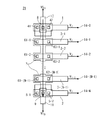
図12は、第4の実施の形態における抵抗ストリング21の等価回路図である。ここでは、第1の実施の形態において説明した抵抗ストリング21と同様な構成の2つの抵抗ストリング21Aと抵抗ストリング21Bが直列に接続された形態が示される。又、第1の実施の形態と同様な構成には、同じ符号にA又はBの符号を付して区別して説明する。更に、ダミー抵抗rdum、及びコンタクト抵抗rcon0〜rconNは、定電流が流れず電圧降下の影響が無視できるため、記載が省略されている。図12を参照して、抵抗ストリング21Aは、参照電圧VG0及びVGNが入力され、これに応じた階調電圧V0A〜VNAをノード14A−0〜14A−Nに供給する。抵抗ストリング21Bは、参照電圧VGN及びVG2Nが入力され、これに応じた階調電圧V0B〜VNBをノード14B−1〜14B−2Nに供給する。抵抗ストリング21Aには、ノード19Aを介して参照電圧VGNが供給される。又、抵抗ストリング21Bは、ノード19Aに接続して、参照電圧VGNが供給されるノード19Bを有する。図12に示されるように、ノード19Aとノード19Bとの間には、抵抗Rtが設けられ、抵抗Rtによって電圧降下された参照電圧がノード19Bに供給されても良い。更に参照電圧VGNは、ノード19Aでなく、ノード19Bに供給されても良い。また、参照電圧VGNがノード19A、19Bのどちらにも供給されず、参照電圧VG0及びVG2Nのみが供給されてもよい。その場合、参照電圧VG0が供給される端子から、抵抗ストリング21A、抵抗Rt、抵抗ストリング21Bを介して参照電圧VG2Nが供給される端子に至る経路に定電流が流れる。
FIG. 12 is an equivalent circuit diagram of the
図12に示される等価回路に対応する抵抗ストリング21のレイアウトパターンを図13に示す。図13を参照して、第4の実施の形態における抵抗ストリング21は、それぞれが、第1の実施の形態と同様なレイアウトパターンの抵抗ストリング21A及び21Bを備える。抵抗ストリング21Aの配線11Aと、抵抗ストリング21Bの配線10Bは、抵抗Rtを介して接続される。詳細には、抵抗値Rtを形成するように抵抗素子7Cにコンタクト8C及び9Cが設けられる。コンタクト8Cは配線11Cを介して配線11Aに接続され、コンタクト9Cは配線10Cを介して配線10Bに接続される。すなわち、配線11Aに供給される参照電圧VGNがコンタクト8C及び9C間で形成される抵抗Rtを経由して抵抗ストリング21Bのコンタクト8Bに供給される。尚、配線10Cと配線11Cは分離して形成される。又、配線11Aと配線11C、配線10Bと配線10Cはそれぞれ同じ配線でも構わない。配線11Bには、参照電圧V2Nが供給される。ここで、参照電圧V2Nは、配線10Bに供給される参照電圧より小さい値である。
FIG. 13 shows a layout pattern of the
このような構成により、抵抗ストリング21Aにおいては、参照電圧に対するコンタクト抵抗rconHA及びrconLAによる電圧降下の影響が、階調電圧V0A〜VNAに均等に作用し、それぞれの相対誤差を抑制する。同様に、抵抗ストリング21Bにおいては、参照電圧に対するコンタクト抵抗rconHB及びrconLBによる電圧降下の影響が、階調電圧V0B〜VNBに均等に作用し、それぞれの相対誤差を抑制する。すなわち、抵抗ストリング21A、21Bのそれぞれにおける階調電圧の相対誤差は抑制される。
With such a configuration, in the
以上のように、本発明は、複数の抵抗ストリング21を有する場合においても、それぞれの抵抗ストリングにおける階調電圧の相対誤差を抑制することができる。 As described above, the present invention can suppress the relative error of the gradation voltage in each resistor string even when the resistor strings 21 are provided.
6.第5の実施の形態
図16及び図17を参照して、抵抗ストリング21の第5の実施の形態を説明する。第5の実施の形態は、第1の実施の形態の変形例(図5及び図6)における抵抗ストリングを複数備えた抵抗ストリングである。また第5の実施の形態は、第4の実施形態(図12及び図13)において、参照電圧VGNが供給されず、参照電圧VG0及びVG2Nのみが供給される場合に好適な抵抗ストリングの構成である。第4の実施形態の図13では、抵抗ストリング21A、21Bのそれぞれにおける階調電圧V0A〜VNA及び階調電圧V0B〜VNBにおける相対誤差は抑制できる。しかし、参照電圧VGNが供給されず、参照電圧VG0及びVG2Nのみが供給される場合、抵抗ストリング21Aと21Bの接続部では電流経路上に抵抗ストリング21Aのコンタクト9A、抵抗素子7Cのコンタクト8C及び9C、抵抗ストリング21Bのコンタクト8Bがあり、4箇所のコンタクト抵抗の電圧降下の影響を受ける。このためコンタクト抵抗のばらつきがあると、階調電圧VNAとV0B間の電位差に相対誤差が生じる可能性がある。第5の実施の形態では、抵抗ストリング間の電位差に対しても相対誤差が抑えられる構成について説明する。
6). Fifth Embodiment With reference to FIGS. 16 and 17, a fifth embodiment of the
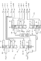
図16は、第5の実施の形態における抵抗ストリング21の等価回路図である。ここでは、第1の実施の形態の変形例(図5及び図6)において説明した抵抗ストリング21と同様な構成の2つの抵抗ストリング21Aと抵抗ストリング21Bが直列で接続された形態が示される。又、図5及び図6と同様な構成には、同じ符号にA又はBの符号を付して区別して説明する。更に、ダミー抵抗rdum、及びコンタクト抵抗rcon0〜rconNは、定電流が流れず電圧降下の影響が無視できるため、記載が省略されている。図16を参照すると、抵抗ストリング21A、21Bに参照電圧VG0及びVGXNがそれぞれ入力され、これに応じた階調電圧V0A〜VNAが抵抗ストリング21Aからノード14A−0〜14A−Nに供給され、階調電圧V0B〜VNBが抵抗ストリング21Bからノード14B−1〜14B−Nに供給される。尚、図5及び図6では抵抗ストリングのN個の抵抗Rは全て同一とされているが、第2に実施形態で説明したように、各抵抗Rは異なる抵抗値でも構わない。したがって第5の実施形態では、抵抗ストリング21AのN個の抵抗をR1A〜RNAとし、抵抗ストリング21BのN個の抵抗をR1B〜RNBとする。抵抗ストリング21A及び21Bは、抵抗ストリング21Aに追加された抵抗R(N+1)Aを介して接続される。抵抗R(N+1)Aの一端はノード18Aに接続され、抵抗R(N+1)Aの他端(ノード19A−1)はコンタクト抵抗rcontLAに接続される。抵抗ストリング21Aのコンタクト抵抗rcontLA(ノード19A−2)と抵抗ストリング21Bのコンタクト抵抗rcontHB(ノード17B−1)が配線(金属配線など)で接続されることにより、抵抗ストリング21A及び21Bが接続される。
FIG. 16 is an equivalent circuit diagram of the
また、抵抗ストリング21Aと抵抗ストリング21Bとを接続する配線の途中に別の抵抗ストリング21Cを備えてもよい。図16において、抵抗ストリング21Cは、抵抗ストリング21Aと同様の構成とされており、同様の構成の素子番号は符号Cを付けて区別する。抵抗ストリング21Cはコンタクト抵抗rcontHCのノード17C−1が配線を介して抵抗ストリング21Aのコンタクト抵抗rcontLAのノード19A−2と接続され、コンタクト抵抗rcontLCのノード19C−1が配線を介して抵抗ストリング21Bのコンタクト抵抗rcontHBのノード17B−1と接続される。定電流は、参照電圧VG0が供給される端子から、抵抗ストリング21A、21C、21Bを介して参照電圧VGXNが供給される端子に至る経路に流れる。抵抗ストリング21Cには参照電圧は入力されず、定電流に応じて階調電圧V0C〜VNCが抵抗ストリング21Cからノード14C−0〜14C−Nに供給される。なお、抵抗ストリング21Cは、抵抗ストリング21Aと21Bの間に直列形態で複数個備えてもよい。
Further, another
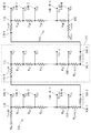
図16に示される等価回路に対応する抵抗ストリング21のレイアウトパターンを図17に示す。図17を参照すると、第5の実施の形態における抵抗ストリング21は、それぞれが、図6と同様なレイアウトパターンの抵抗ストリング21A及び21Bを備える。図17と図6のレイアウトパターンの相違点は、図6では配線11と接続するコンタクト9が配線2に接続されるコンタクト5の近傍に配置されるが、図17では配線11A−1と接続するコンタクト9A−1が配線2Aに接続されるコンタクト5A近傍から抵抗R(N+1)Aだけ抵抗素子7Aが伸長された位置に配置される。抵抗ストリング21Aの配線11A−1は抵抗ストリング21Bの配線10Bと接続されることで、抵抗ストリング21Aと抵抗ストリング21Bが接続される。好ましくは配線11A−1と10Bは同一配線とされる。
FIG. 17 shows a layout pattern of the
又、抵抗ストリング21Aと抵抗ストリング21Bの間に、抵抗ストリング21Cを配置してもよい。図17では、抵抗ストリング21Cは抵抗ストリング21Aと同様のレイアウトパターンとされている。この場合、抵抗ストリング21Cの配線10Cが抵抗ストリング21Aの配線11A−1に接続され、配線11C−1が抵抗ストリング21Bの配線10Bに接続される。好ましくは配線11A−1と10Cは同一配線とされ、配線11C−1と10Bも同一配線とされる。
Further, the
図16及び図17において、抵抗ストリング21A、21Bが接続される場合(抵抗ストリング21Cがない場合)、抵抗ストリング21Aと21Bの接続部では定電流の電流経路上には抵抗ストリング21Aのコンタクト9A−1と抵抗ストリング21Bのコンタクト8Bだけで、コンタクト抵抗の電圧降下は2箇所に減る。したがって本実施の形態では第4の実施形態(図13)の場合よりも抵抗ストリング21A、21B間のコンタクト抵抗の影響が小さく、階調電圧VNAとV0B間の電位差の相対誤差を抑制できる。なお、抵抗ストリング21Aの抵抗R(N+1)Aは、抵抗R1A〜RNAと同一の抵抗素子7Aに形成されており、抵抗R1A〜R(N+1)Aの抵抗分割により生成される階調電圧Vの相対誤差は小さい。抵抗ストリング21Aの階調電圧VNAと抵抗ストリング21Aの階調電圧V0Bの電位差は抵抗R(N+1)Aで設定される。なお、抵抗R(N+1)Aを分割して、抵抗素子7Aと7Bに分けて形成し、分割した抵抗間でコンタクト9A−1、8B及び配線11A−1(10B)を介して接続する構成にしてもよい。また、抵抗ストリング21A、21B間に抵抗ストリング21Cが接続される場合についても、各抵抗ストリング間の接続部で定電流が流れるコンタクト抵抗は2箇所だけである。したがって、各抵抗ストリング間の階調電圧の相対誤差が抑制できる。なお、抵抗ストリング21Aと21Cの階調電圧VNA、V0C間の電位差は抵抗R(N+1)Aで設定され、抵抗ストリング21Cと21Bの階調電圧VNC、V0B間の電位差は抵抗R(N+1)Cで設定される。抵抗R(N+1)A、R(N+1)Cは、それぞれ2つの抵抗素子間に分割して設けてもよい。
16 and 17, when the
以上のように、本発明は、複数の抵抗ストリング21を有する場合においても、それぞれの抵抗ストリングにおける階調電圧の相対誤差、及び、抵抗ストリング間の階調電圧の相対誤差を抑制することができる。 As described above, the present invention can suppress the relative error of the grayscale voltage in each resistor string and the relative error of the grayscale voltage between the resistor strings even when the resistor strings 21 are provided. .
本発明によれば、階調電圧の最大値(V0)及び最小値(VN)が供給されるコンタクト5及び6を、抵抗ストリング21内を流れる定電流Iの電流経路から外れた領域に設けることで、コンタクト抵抗による階調電圧間の相対誤差を抑制することができる。このため、本発明を液晶表示装置に適用した場合、表示パネルの表示ムラを抑制することができる。又、コンタクト抵抗による階調電圧への影響を排除しているため、歩留まりを向上させることが可能となる。又、本発明を液晶表示装置に適用する場合、液晶パネルのガンマ特性に応じて参照電圧を変調する場合があるが、その場合でも、階調電圧V1〜VN−1の相対精度は維持される。
According to the present invention, the
以上、本発明の実施の形態を詳述してきたが、具体的な構成は上記実施の形態に限られるものではなく、本発明の要旨を逸脱しない範囲の変更があっても本発明に含まれる。上述の実施例では、階調電圧を取り出すためのコンタクトや参照電圧が供給されるコンタクトはそれぞれ1つ(変形例では2つ)で説明したが、それぞれ複数個設けられても構わない。又、本実施の形態では、液晶表示装置に利用される階調電圧発生回路を一例に説明したが、ADコンバータ又はDAコンバータや、複数のレベル電圧を利用するセンサ等の回路に利用できることは言うまでもない。 The embodiment of the present invention has been described in detail above, but the specific configuration is not limited to the above-described embodiment, and changes within a scope not departing from the gist of the present invention are included in the present invention. . In the above-described embodiments, one contact for extracting the gradation voltage and one contact to which the reference voltage is supplied have been described (two in the modification), but a plurality of contacts may be provided. In this embodiment, the gradation voltage generation circuit used in the liquid crystal display device has been described as an example. However, it goes without saying that it can be used in circuits such as an AD converter or a DA converter, or a sensor using a plurality of level voltages. Yes.
1、2、3−1〜3−N、51、52、53−1〜53−N、10〜13:配線
4、41、42、4A、4B:コンタクトMAX
5、5−1、5−2、5A、5B:コンタクトMIN
6−1〜6−N、8、9、54−0〜54−N、61−1〜61−N、62−1〜62N、6A−1〜6A−N、6B−1〜6B−N:コンタクト
7、55:抵抗素子
14−0〜14−N、14A−0〜14A−N、14B−0〜14B−N、17、17B、18、18A、19A,19B、56−0〜56−N:ノード
15:ダミー配線
16:ダミーコンタクト
20:データドライバ
21、21A、21B、21C、50:抵抗ストリング
22:階調電圧発生回路
23:ラッチアドレスセレクタ
24:ラッチ
25:デコーダ
26:増幅器
30:ゲートドライバ
40:表示パネル
P:画素
43:液晶容量
44:画素電極
45:対向電極
46:データ線
47:走査線
48:TFT
100:液晶表示装置
VG0、VGN:参照電圧
V0〜VN:階調電圧
Vout:表示信号
R、Rt:抵抗
rconH、rconHA、rconHB、rconHC、rconL、rconLA、rconLB、rconLC、rcon0〜rconN:コンタクト抵抗
1, 2, 3-1 to 3-N, 51, 52, 53-1 to 53-N, 10 to 13:
5, 5-1, 5-2, 5A, 5B: contact MIN
6-1 to 6-N, 8, 9, 54-0 to 54-N, 61-1 to 61-N, 62-1 to 62N, 6A-1 to 6A-N, 6B-1 to 6B-N:
100: Liquid crystal display device VG 0 , VG N : Reference voltage V 0 to V N : Gradation voltage V out : Display signal R, R t : Resistance r conH , r conHA , r conHB , r conHC , r conL , r conLA , r conLB, r conLC, r con0 ~r conN: contact resistance
Claims (15)
抵抗体と、
第1の参照電圧が供給される第1の導電体と、
第2の参照電圧が供給される第2の導電体と、
前記複数のレベル電圧のうち前記第1の参照電圧に最も近い値の第1のレベル電圧が出力される第3の導電体と、
前記第1のレベル電圧とは別の第2のレベル電圧が出力される第4の導電体と、
前記第1の導電体と前記抵抗体とを結合して導通可能とする第1の接続部と、
前記第2の導電体と前記抵抗体とを結合して導通可能とする第2の接続部と、
前記第3の導電体と前記抵抗体とを結合して導通可能とする第3の接続部と、
前記第4の導電体と前記抵抗体とを結合して導通可能とする第4の接続部と、
を具備し、
前記第1乃至第4の導電体のそれぞれは互いに分離し、
前記第3の接続部、前記第1の接続部、前記第4の接続部、前記第2の接続部は、直列形態の第1から第3の抵抗領域を形成するように、前記抵抗体に順次配置され、
前記第1の抵抗領域を介した前記第3の接続部と前記第1の接続部の間隔は、前記第2の抵抗領域を介した前記第1の接続部と前記第4の接続部の間隔、及び、前記第3の抵抗領域を介した前記第4の接続部と前記第2の接続部の間隔に比べて充分小さいマルチレベル電圧発生器。 A plurality of level voltages corresponding to the supplied first reference voltage and second reference voltage are generated, and a plurality of conductors that output the plurality of level voltages are capacitive on the input side of the amplifier via a decoder. A multi-level voltage generator connected to a load,
A resistor,
A first conductor supplied with a first reference voltage;
A second conductor supplied with a second reference voltage;
A third conductor that outputs a first level voltage having a value closest to the first reference voltage among the plurality of level voltages;
A fourth conductor from which a second level voltage different from the first level voltage is output;
A first connecting portion that couples the first conductor and the resistor to enable conduction;
A second connecting portion that couples the second conductor and the resistor to enable conduction;
A third connection portion that couples the third conductor and the resistor to enable conduction;
A fourth connection portion that couples the fourth conductor and the resistor to enable conduction;
Comprising
Each of the first to fourth conductors is separated from each other ,
Third connection portion prior to reporting, the first connecting portion, the fourth connecting portion, said second connecting portion, the first series configuration so as to form a third resistor region, the resistor Are arranged sequentially ,
An interval between the third connection portion and the first connection portion via the first resistance region is an interval between the first connection portion and the fourth connection portion via the second resistance region. And a multi-level voltage generator that is sufficiently smaller than an interval between the fourth connection portion and the second connection portion via the third resistance region .
前記複数のレベル電圧のうち前記第2の参照電圧に最も近い値の第3のレベル電圧が出力される第5の導電体と、
前記第5の導電体と前記抵抗体とを結合して導通可能とする第5の接続部と、
を更に具備し、
前記第5の接続部は、前記第2の接続部との間に第4の抵抗領域を形成するように前記抵抗体に配置され、
前記第4の抵抗領域を介した前記第5の接続部と前記第2の接続部の間隔は、前記第2の抵抗領域を介した前記第1の接続部と前記第4の接続部の間隔、及び、前記第3の抵抗領域を介した前記第4の接続部と前記第2の接続部の間隔に比べて充分小さいマルチレベル電圧発生器。 The multilevel voltage generator of claim 1.
A fifth conductor that outputs a third level voltage having a value closest to the second reference voltage among the plurality of level voltages;
A fifth connection portion that couples the fifth conductor and the resistor to enable conduction;
Further comprising,
Before fifth connection portion SL is disposed on the resistor so as to form a fourth resistance region between said second connecting portion,
The interval between the fifth connection portion and the second connection portion via the fourth resistance region is the interval between the first connection portion and the fourth connection portion via the second resistance region. And a multi-level voltage generator that is sufficiently smaller than an interval between the fourth connection portion and the second connection portion via the third resistance region .
前記複数のレベル電圧のうち前記第1、前記第2のレベル電圧とは異なるレベル電圧群が出力される複数の導電体と、
前記複数の導電体と前記抵抗体とをそれぞれ結合して導通可能とする複数の接続部と、
を更に具備し、
前記複数の接続部は、前記第1及び第4の接続部との間に配置され、前記第1及び第4の接続部との間に形成される前記第2の抵抗領域を、更に複数の抵抗領域に分割するマルチレベル電圧発生器。 The multilevel voltage generator of claim 1.
A plurality of conductors that output a level voltage group different from the first and second level voltages among the plurality of level voltages;
A plurality of connecting portions that connect the plurality of conductors and the resistor to enable conduction;
Further comprising
The plurality of connection portions are disposed between the first and fourth connection portions, and the second resistance region formed between the first and fourth connection portions is further provided with a plurality of connection portions. Multi-level voltage generator that divides into resistive areas.
前記第4の接続部及び前記複数の接続部は、前記抵抗体において、前記第1の接続部と前記第2の接続部とを結ぶ最短経路上に配置される
マルチレベル電圧発生器。 The multilevel voltage generator of claim 3.
The fourth connection section and the plurality of connection sections are multi-level voltage generators arranged on a shortest path connecting the first connection section and the second connection section in the resistor.
前記第4の接続部及び前記複数の接続部は、前記抵抗体において、前記第1の接続部と前記第2の接続部とを結ぶ最短経路上から外れた位置に配置される
マルチレベル電圧発生器。 The multilevel voltage generator of claim 3.
The fourth connecting portion and the plurality of connecting portions are arranged at positions away from the shortest path connecting the first connecting portion and the second connecting portion in the resistor. vessel.
前記第1乃至第4の導電体は、それぞれ金属材料で形成されるマルチレベル電圧発生器。 A multi-level voltage generator according to any one of claims 1 to 5,
Each of the first to fourth conductors is a multi-level voltage generator formed of a metal material.
第1及び第2の抵抗体と、
第1の参照電圧が供給される第1の導電体と、
第2の参照電圧が供給される第2の導電体と、
前記第1及び第2の抵抗体を接続する第3及び第4の導電体と、
前記複数のレベル電圧において第1至乃第4のレベル電圧がそれぞれ出力される第5至乃第8の導電体と、
前記第1の導電体と前記第1の抵抗体とを結合して導通可能とする第1の接続部と、
前記第2の導電体と前記第2の抵抗体とを結合して導通可能とする第2の接続部と、
前記第3の導電体と前記第1の抵抗体とを結合して導通可能とする第3の接続部と、
前記第4の導電体と前記第2の抵抗体とを結合して導通可能とする第4の接続部と、
前記第5及び前記第6の導電体のそれぞれと前記第1の抵抗体とを結合して導通可能とする第5及び第6の接続部と、
前記第7及び前記第8の導電体のそれぞれと前記第2の抵抗体とを結合して導通可能とする第7及び第8の接続部と、
を具備し、
前記第1の抵抗体に結合される前記第1、前記第3、前記第5、前記第6の導電体のそれぞれは互いに分離し、
前記第2の抵抗体に結合される前記第2、前記第4、前記第7、前記第8の導電体のそれぞれは互いに分離し、
前記第5の接続部、前記第1の接続部、前記第6の接続部、前記第3の接続部が、直列形態の第1から第3の抵抗領域を形成するように、前記第1の抵抗体に順次配置され、
前記第7の接続部、前記第4の接続部、前記第8の接続部、前記第2の接続部が、直列形態の第4から第6の抵抗領域を形成するように、前記第2の抵抗体に順次配置され、
前記第1の抵抗領域を介した前記第5の接続部と前記第1の接続部の間隔は、前記第2の抵抗領域を介した前記第1の接続部と前記第6の接続部の間隔、及び、前記第3の抵抗領域を介した前記第6の接続部と前記第3の接続部の間隔に比べて充分小さく、
前記第4の抵抗領域を介した前記第7の接続部と前記第4の接続部の間隔は、前記第5の抵抗領域を介した前記第4の接続部と前記第8の接続部の間隔、及び、前記第6の抵抗領域を介した前記第8の接続部と前記第2の接続部の間隔に比べて充分小さいマルチレベル電圧発生器。 To generate a plurality of level voltages corresponding to the first and second reference voltages supplied, via a plurality of electrical conductors decoder for outputting said plurality of level voltages connected to the capacitive load on the input side of the amplifier A multi-level voltage generator
First and second resistors;
A first conductor supplied with a first reference voltage;
A second conductor supplied with a second reference voltage;
Third and fourth conductors connecting the first and second resistors;
A fifth to eighth conductor from which a first to fourth level voltage is output at each of the plurality of level voltages;
A first connecting portion that couples the first conductor and the first resistor to enable conduction;
A second connection portion that couples the second conductor and the second resistor to enable conduction;
A third connection portion that couples the third conductor and the first resistor to enable conduction;
A fourth connecting portion that couples the fourth conductor and the second resistor to enable conduction;
5th and 6th connection parts which connect each of said 5th and said 6th electric conductors and said 1st resistor, and can conduct, and
Seventh and eighth connection portions that connect each of the seventh and eighth conductors and the second resistor to enable conduction;
Comprising
Each of the first, third, fifth, and sixth conductors coupled to the first resistor are separated from each other;
Each of the second, fourth, seventh, and eighth conductors coupled to the second resistor are separated from each other ;
Connecting portions of the front Symbol fifth, the first connection portion, the connection portion of the sixth, as the third connecting portions, to the first series form a third resistor region, said first Are placed sequentially on the resistors ,
Before SL connecting portion of the seventh, the fourth connection portion, the connection portion of the eighth, as the second connecting portion, to the fourth series morphogenesis resistance region of the sixth, the second Are placed sequentially on the resistors ,
The interval between the fifth connection portion and the first connection portion via the first resistance region is the interval between the first connection portion and the sixth connection portion via the second resistance region. And sufficiently smaller than the distance between the sixth connection part and the third connection part via the third resistance region,
The interval between the seventh connection portion and the fourth connection portion via the fourth resistance region is the interval between the fourth connection portion and the eighth connection portion via the fifth resistance region. And a multi-level voltage generator that is sufficiently smaller than an interval between the eighth connection portion and the second connection portion via the sixth resistance region .
前記第3の導電体と前記第4の導電体との間に接続される第3の抵抗体を更に具備し、
前記第3の導電体又は前記第4の導電体のいずれか一方に第3の参照電圧が供給されるマルチレベル電圧発生器。 The multi-level voltage generator of claim 7,
A third resistor connected between the third conductor and the fourth conductor;
A multi-level voltage generator in which a third reference voltage is supplied to either the third conductor or the fourth conductor.
前記第4の導電体は前記第3の導電体と同一とされるマルチレベル電圧発生器。 The multi-level voltage generator of claim 7,
The multi-level voltage generator, wherein the fourth conductor is the same as the third conductor.
前記第3の導電体と前記第4の導電体との間に直列形態で接続される複数の抵抗体を更に具備するマルチレベル電圧発生器。 The multi-level voltage generator of claim 7,
A multi-level voltage generator further comprising a plurality of resistors connected in series between the third conductor and the fourth conductor.
第5のレベル電圧が出力される第9の導電体と、
前記第9の導電体と前記第2の抵抗体とを結合して導通可能とする第9の接続部と、
を更に具備し、
前記第9の接続部は、前記第2の接続部との間に第7の抵抗領域を形成するように前記第2の抵抗体に配置され、前記第7の抵抗領域を介した前記第2の接続部と前記第9の接続部の間隔は、前記第5の抵抗領域を介した前記第4の接続部と前記第8の接続部の間隔、及び、前記第6の抵抗領域を介した前記第8の接続部と前記第2の接続部の間隔に比べて充分小さいマルチレベル電圧発生器。 The multi-level voltage generator according to any one of claims 7 to 10,
A ninth conductor from which a fifth level voltage is output;
A ninth connecting portion that couples the ninth conductor and the second resistor to enable conduction;
Further comprising,
Before SL connections ninth, the between the second connecting portion is disposed in said so as to form a resistive region of the seventh second resistor, the first through the seventh resistor region of The interval between the second connection portion and the ninth connection portion is the interval between the fourth connection portion and the eighth connection portion via the fifth resistance region, and via the sixth resistance region. A multi-level voltage generator that is sufficiently smaller than the distance between the eighth connection and the second connection .
前記第3の導電体と前記第4の導電体との間に接続される前記複数の抵抗体のうち前記第3の導電体と接続される第3の抵抗体と、
第5及び第6のレベル電圧がそれぞれ出力される第9及び第10の導電体と、
前記第3の導電体と前記第3の抵抗体とを結合して導通可能とする第9の接続部と、
前記第9の導電体と前記第3の抵抗体とを結合して導通可能とする第10の接続部と、
前記第10の導電体と前記第3の抵抗体とを結合して導通可能とする第11の接続部と、を更に具備し、
前記10の接続部、前記第9の接続部、前記第11の接続部が、直列形態の第7及び第8の抵抗領域を形成するように、前記第3の抵抗体に順次配置され、前記第7の抵抗領域を介した前記第10の接続部と前記第9の接続部の間隔は、前記第8の抵抗領域が形成された前記第9の接続部と前記第11の接続部の間隔に比べて充分小さいマルチレベル電圧発生器。 The multi-level voltage generator of claim 10.
A third resistor connected to the third conductor among the plurality of resistors connected between the third conductor and the fourth conductor;
Ninth and tenth conductors from which fifth and sixth level voltages are output, respectively;
A ninth connecting portion that couples the third conductor and the third resistor to enable conduction;
A tenth connecting portion that couples the ninth conductor and the third resistor to enable conduction;
An eleventh connection portion that couples the tenth conductor and the third resistor to enable conduction ;
Connecting portions of the front SL 10, connecting portions of the ninth, connecting portions of the first 11, so as to form a seventh and resistance region of the eighth series configuration, it is sequentially disposed on the third resistor, The interval between the tenth connection portion and the ninth connection portion via the seventh resistance region is the same as that between the ninth connection portion and the eleventh connection portion where the eighth resistance region is formed. Multilevel voltage generator that is sufficiently small compared to the interval .
前記複数のレベル電圧のうち前記第1、前記第2のレベル電圧と異なる第1のレベル電圧群が出力される第1の導電体群と、
前記複数のレベル電圧のうち前記第3、前記第4のレベル電圧と異なる第2のレベル電圧群が出力される第2の導電体群と、
前記第1の導電体群と前記第1の抵抗体とをそれぞれ結合して導通可能とする第1の接続部群と、
前記第2の導電体群と前記第2の抵抗体とをそれぞれ結合して導通可能とする第2の接続部群と、
を更に具備し、
前記第1の接続部群は、前記第1の接続部と前記第6の接続部との間に配置され、前記第1及び前記第6の接続部との間に形成される前記第2の抵抗領域を、更に複数の抵抗領域に分割し、
前記第2の接続部群は、前記第4の接続部と前記第8の接続部との間に配置され、前記第4及び前記第8の接続部との間に形成される前記第5の抵抗領域を、更に複数の抵抗領域に分割するマルチレベル電圧発生器。 The multi-level voltage generator according to any one of claims 7 to 12,
A first conductor group that outputs a first level voltage group different from the first and second level voltages among the plurality of level voltages;
A second conductor group that outputs a second level voltage group different from the third and fourth level voltages among the plurality of level voltages;
A first connection portion group that allows the first conductor group and the first resistor to be coupled to each other to be conductive;
A second connection portion group that couples the second conductor group and the second resistor to enable conduction;
Further comprising
The first connection portion group is disposed between the first connection portion and the sixth connection portion, and is formed between the first and sixth connection portions. The resistance region is further divided into a plurality of resistance regions,
The second connecting portion group is disposed between the fourth connecting portion and the eighth connecting portion, and is formed between the fourth and eighth connecting portions. A multi-level voltage generator that further divides a resistance region into a plurality of resistance regions.
入力されるデジタルデータに応じて前記マルチレベル電圧発生器から出力されるレベル電圧を選択するデコーダと、
前記デコーダで選択されたレベル電圧を増幅出力する増幅器と、
を具備するデータドライバ。 A multi-level voltage generator according to any one of claims 1 to 13,
A decoder for selecting a level voltage output from the multi-level voltage generator according to input digital data;
An amplifier for amplifying and outputting the level voltage selected by the decoder;
A data driver comprising:
走査線と前記データ線とに接続された画素を有する表示パネルと、
前記走査線を駆動するゲートドライバと
を具備する液晶表示装置。 A data driver according to claim 14;
A display panel having pixels connected to scanning lines and the data lines;
A liquid crystal display device comprising a gate driver for driving the scanning line.
Priority Applications (3)
| Application Number | Priority Date | Filing Date | Title |
|---|---|---|---|
| JP2007281525A JP5117817B2 (en) | 2006-11-02 | 2007-10-30 | Multi-level voltage generator, data driver, and liquid crystal display device |
| US11/979,351 US8094109B2 (en) | 2006-11-02 | 2007-11-01 | Data driver with multilevel voltage generating circuit, and liquid crystal display apparatus including layout pattern of resistor string of the multilevel generating circuit |
| CN2007101692245A CN101221329B (en) | 2006-11-02 | 2007-11-02 | Data driver with multilevel voltage generating circuit, and liquid crystal display apparatus |
Applications Claiming Priority (3)
| Application Number | Priority Date | Filing Date | Title |
|---|---|---|---|
| JP2006298551 | 2006-11-02 | ||
| JP2006298551 | 2006-11-02 | ||
| JP2007281525A JP5117817B2 (en) | 2006-11-02 | 2007-10-30 | Multi-level voltage generator, data driver, and liquid crystal display device |
Publications (2)
| Publication Number | Publication Date |
|---|---|
| JP2008146028A JP2008146028A (en) | 2008-06-26 |
| JP5117817B2 true JP5117817B2 (en) | 2013-01-16 |
Family
ID=39606233
Family Applications (1)
| Application Number | Title | Priority Date | Filing Date |
|---|---|---|---|
| JP2007281525A Expired - Fee Related JP5117817B2 (en) | 2006-11-02 | 2007-10-30 | Multi-level voltage generator, data driver, and liquid crystal display device |
Country Status (2)
| Country | Link |
|---|---|
| JP (1) | JP5117817B2 (en) |
| CN (1) | CN101221329B (en) |
Families Citing this family (1)
| Publication number | Priority date | Publication date | Assignee | Title |
|---|---|---|---|---|
| JP7286498B2 (en) * | 2019-09-24 | 2023-06-05 | ラピスセミコンダクタ株式会社 | Level voltage generation circuit, data driver and display device |
Family Cites Families (10)
| Publication number | Priority date | Publication date | Assignee | Title |
|---|---|---|---|---|
| JPS5780702A (en) * | 1980-11-10 | 1982-05-20 | Matsushita Electric Industrial Co Ltd | Thin film radar resistor network circuit |
| JPS59104159A (en) * | 1982-12-07 | 1984-06-15 | Nec Corp | Resistance row voltage dividing circuit |
| JPH0563145A (en) * | 1990-11-08 | 1993-03-12 | Nec Corp | Resistance element |
| JP3113031B2 (en) * | 1992-01-31 | 2000-11-27 | 株式会社東芝 | Parallel A / D converter |
| JPH07240839A (en) * | 1994-02-28 | 1995-09-12 | Toshiba Corp | Image processing device |
| JP3847423B2 (en) * | 1997-09-04 | 2006-11-22 | 株式会社ルネサステクノロジ | Constant voltage generator |
| JP2000208703A (en) * | 1999-01-08 | 2000-07-28 | Seiko Epson Corp | Semiconductor integrated circuit |
| JP2005010276A (en) * | 2003-06-17 | 2005-01-13 | Seiko Epson Corp | Gamma correction circuit, liquid crystal drive circuit, display device, power supply circuit |
| US20080246712A1 (en) * | 2005-01-18 | 2008-10-09 | Nxp B.V. | Programmable Gray Level Generation Unit |
| JP4836469B2 (en) * | 2005-02-25 | 2011-12-14 | ルネサスエレクトロニクス株式会社 | Gradation voltage generator |
-
2007
- 2007-10-30 JP JP2007281525A patent/JP5117817B2/en not_active Expired - Fee Related
- 2007-11-02 CN CN2007101692245A patent/CN101221329B/en not_active Expired - Fee Related
Also Published As
| Publication number | Publication date |
|---|---|
| CN101221329A (en) | 2008-07-16 |
| JP2008146028A (en) | 2008-06-26 |
| CN101221329B (en) | 2012-11-21 |
Similar Documents
| Publication | Publication Date | Title |
|---|---|---|
| US11200864B2 (en) | Level voltage generation circuit, data driver, and display apparatus | |
| JP4472737B2 (en) | Semiconductor device, semiconductor element and substrate | |
| US6982706B1 (en) | Liquid crystal driving circuit, semiconductor integrated circuit device, reference voltage buffering circuit, and method for controlling the same | |
| JP3411494B2 (en) | Driving voltage generation circuit for matrix type display device | |
| CN112835217B (en) | Display device and driving method thereof | |
| US9502352B2 (en) | Semiconductor wiring patterns | |
| JP2020525807A (en) | Array substrate and display device | |
| JP3270220B2 (en) | Display device and integrated circuit for driving the same | |
| JP4538712B2 (en) | Display device | |
| US8094109B2 (en) | Data driver with multilevel voltage generating circuit, and liquid crystal display apparatus including layout pattern of resistor string of the multilevel generating circuit | |
| JP3235893B2 (en) | Drive circuit for liquid crystal display | |
| JP2008146028A (en) | Multilevel voltage generator, data driver, and liquid crystal display apparatus | |
| KR100719994B1 (en) | Array substrate for flat display device | |
| US8310425B2 (en) | Resistance dividing circuit | |
| JP5711198B2 (en) | Semiconductor device |
Legal Events
| Date | Code | Title | Description |
|---|---|---|---|
| A621 | Written request for application examination |
Free format text: JAPANESE INTERMEDIATE CODE: A621 Effective date: 20100517 |
|
| A131 | Notification of reasons for refusal |
Free format text: JAPANESE INTERMEDIATE CODE: A131 Effective date: 20120518 |
|
| A521 | Written amendment |
Free format text: JAPANESE INTERMEDIATE CODE: A523 Effective date: 20120717 |
|
| A131 | Notification of reasons for refusal |
Free format text: JAPANESE INTERMEDIATE CODE: A131 Effective date: 20120803 |
|
| A521 | Written amendment |
Free format text: JAPANESE INTERMEDIATE CODE: A523 Effective date: 20120927 |
|
| TRDD | Decision of grant or rejection written | ||
| A01 | Written decision to grant a patent or to grant a registration (utility model) |
Free format text: JAPANESE INTERMEDIATE CODE: A01 Effective date: 20121016 |
|
| A01 | Written decision to grant a patent or to grant a registration (utility model) |
Free format text: JAPANESE INTERMEDIATE CODE: A01 |
|
| A61 | First payment of annual fees (during grant procedure) |
Free format text: JAPANESE INTERMEDIATE CODE: A61 Effective date: 20121018 |
|
| R150 | Certificate of patent or registration of utility model |
Free format text: JAPANESE INTERMEDIATE CODE: R150 |
|
| FPAY | Renewal fee payment (event date is renewal date of database) |
Free format text: PAYMENT UNTIL: 20151026 Year of fee payment: 3 |
|
| S531 | Written request for registration of change of domicile |
Free format text: JAPANESE INTERMEDIATE CODE: R313531 |
|
| R350 | Written notification of registration of transfer |
Free format text: JAPANESE INTERMEDIATE CODE: R350 |
|
| LAPS | Cancellation because of no payment of annual fees |